
 Open Access Article
 This Open Access Article is licensed under a Creative Commons Attribution-Non Commercial 3.0 Unported Licence
Cobalt-doped zinc oxide based memristors with nociceptor characteristics for bio-inspired technology†
Naveed Ur Rehmana,
Aziz Ullaha,
Muhammad Adil Mahmooda,
Nasir Rahman a,
Mohammad Sohaila,
Shahid Iqbalb,
Nizomiddin Juraevcd,
Khaled Althubeitie,
Sattam Al Otaibif and
Rajwali Khan*ag
a,
Mohammad Sohaila,
Shahid Iqbalb,
Nizomiddin Juraevcd,
Khaled Althubeitie,
Sattam Al Otaibif and
Rajwali Khan*ag
aDepartment of Physics, University of Lakki Marwat, Lakki Marwat, 2842, KP, Pakistan. E-mail: rajwalipak@zju.edu.cn
bDepartment of Physics, University of Wisconsin, La Crosse, WI, 54601, USA
cFaculty of Chemical Engineering, New Uzbekistan University, Tashkent, Uzbekistan
dScientific and Innovation Department, Tashkent State Pedagogical University, Tashkent, Uzbekistan
eDepartment of Chemistry, College of Science, Taif University, P.O. BOX. 110, 21944 Taif, Saudi Arabia
fDepartment of Electrical Engineering, College of Engineering Taif University, P.O. Box 11099, Taif, 21944, Saudi Arabia
gDepartment of Physics, United Arab Emirates University, Al Ain, 15551, Abu Dhabi, UAE
First published on 12th April 2024
Abstract
Neuromorphic computing is a new field of information technology, which is inspired by the biomimetic properties of the memristor as an electronic synapse and neuron. If there are electronic receptors that can transmit exterior impulses to the internal nervous system, then the use of memristors can be expanded to artificial nerves. In this study, a layer type memristor is used to build an artificial nociceptor in a very feasible and straightforward manner. An artificial nociceptor is demonstrated here through the fabrication and characterization of a cobalt-doped zinc oxide (CZO)/Au based memristor. In order to increase threshold switching performance, the surface effects of the CZO layer are eliminated by adding cobalt cobalt-doped zinc oxide (CZO) layer between the P++-Si and Au electrodes. Allodynia, hyperalgesia, threshold, and relaxation are the four distinct nociceptive behaviours that the device displays based on the strength, rate of relapse, and duration of the external stimuli. The electrons that are trapped in or released from the CZO layer's traps are responsible for these nociceptive behaviours. A multipurpose nociceptor performance is produced by this type of CZO-based device, which is crucial for artificial intelligence system applications such as neural integrated devices with nanometer-sized characteristics.
1 Introduction
The discovery and creation of new types of memory devices have encouraged numerous research activities in recent years since traditional memory cannot keep up with the demands of rising data capacity and processing speed.1,2 To the best of our knowledge, resistive random-access memory (RRAM) is a promising memory device that has enjoyed attention as a potential contender for next-generation devices,3 This is because of its many good qualities, such as its small switching voltage,4 low power consumption, quick switching speed,5 basic design structure, substantial potential for use in synthetic synapses, analog circuits, and high storage density,6 etc. Recently, the memristor devices also referred to as the fourth essential circuit element, was created by utilizing the resistive switching (RS) effect.2 Future memory devices can use the RS property of memristors,7 for logic,8 brain-inspired computing systems,9 and sensor applications.10 Numerous materials, including complex oxides,11,12 organics,13 and binary metal oxides14 etc. have shown the RS characteristics. Among various material systems, RRAM devices having insulating layers of metal oxides such as HfO2, AlO3,15 ZnO,16 TiO2,17 and Fe2O3 18 have been widely investigated because of their greater RS performances and compatibility with complementary metal-oxide semiconductor (CMOS) processing. The capacity of memristors to store and recall information through resistance modulation allows them to replicate the adaptive nature of synapses. This feature is pivotal for creating artificial neural networks that can exhibit behavior similar to the brain's synaptic connections.9 Memory, nonlinearity, passivity, a two-terminal construction, and scalability are just a few of the distinctive qualities that the memristor or memristive device possesses.19 The goal of neuromorphic computing and their details are mention in ESI.†Due to the existence of oxygen vacancies, Zinc Oxide (ZnO) exhibits n-type semiconducting activity and is a versatile semiconducting material.20 Excellent RS capabilities have been demonstrated with ZnO in recent years21 Furthermore, ZnO-based devices are used to exhibit flexible,22 transparent,23 and soft24 features. Additionally, ZnO-based devices are frequently utilized to replicate the functions of actual synapses and neurons. ZnO is a type of metal oxide material, which demonstrates exceptional qualities among other metal oxide materials, including a broad direct band gap, low synthetic temperature, low cost, and customizable doping. Its physical properties may be changed by doping various elements into it. Defects' impact on the RS effect has been well studied, and it is widely acknowledged that they play a substantial role. A substantial body of research suggests that metal oxide thin films generally exhibit the defects-induced RS effect.25 Therefore, the impact of flaws must be taken into account when producing RS memory devices. One frequently used approach for the deposition of oxide films is sputtering. Additionally, it was possible to modify the temperature and reactive gas flow ratio during the film deposition stage in order to adjust the properties of ZnO thin films.26,27 To adjust the defect concentration in ZnO films, however, the elements doping approach is more successful than varying the sputtering parameters and deposition temperature.28 According to Xu et al.29 more VO in Co-doped ZnO increases strength and decreases set voltage, suggesting that co-doping can improve RS behavior. Similar findings by Younis et al.30 showed that Ti doping can improve RS performance, showing that the HRS/LRS ratio of Ti-doped ZnO was superior to that of undoped ZnO. With the addition of a Cr dopant, Xu et al.31 similarly showed an upgrade in the on/off ratio and steady RS behavior in ZnO. Transition metals have been added to ZnO, in particular, as a technique for creating multifunctional semiconductor materials suited for next-generation memory systems.32 Based on electrochemical properties, the electrode categories of inert, oxidizable, and active metals are frequently grouped with a switching material. An inert electrode (IE) like Pt, Au, or Ru may function as a cathode and produce a high interface barrier, producing RS characteristics.33 The increased ON/OFF ratio was attributable to the inert electrodes' high work function.34 Even though the electrode has a large work function, its strong electrochemical behaviour and inert behaviour result in an efficient redox process. Regrettably, there are limits to how much oxygen can be maintained in an inert electrode.35
In the current study, we developed a P++-Si/CZO/Au (CZO-Co-doped ZnO) memristive device to demonstrate the nociceptive feature, which is basically distinct from threshold switching, relaxation time, allodynia, and hyperalgesia. Here, asymmetrical capacitive coupled threshold switching behavior is achieved via I–V sweeping at a steady sweep rate on P++-Si & Au electrodes. The main reason of Au as a top electrode, Au has excellent electrical conductivity, which ensures that electrical impulses are transmitted efficiently within the memristor-based artificial nociceptor. This conductivity is critical for the device's correct operation, letting it to reliably respond to external stimuli and display the required nociceptive behaviors. In addition, Au is well-known for its chemical stability and biocompatibility, both of which are important factors in neural-inspired computing applications. These qualities reduce the danger of deterioration or unfavorable responses, which might jeopardize the artificial nociceptor's function or safety when interacting with biological systems. Furthermore, Au compatibility with common fabrication techniques improves device manufacture and integration into neuromorphic computing systems, adding to its viability and ease of deployment. A switch from low-bias Schottky emission to high-bias trap-aided quantum tunnelling (TAT) governs the switching behavior. The identical experimental procedures utilized to create the P++-Si/CZO/Au memristor device were also employed to create a P++-Si/ZnO/Au device for comparison. In contrast to ZnO-based memristors, the CZO-based memristor displays threshold switching and resistance switching features in response to electrical stimulation. The experimental results show that the dynamic charge trapping and detrapping of charge carriers, as well as the low activation energies are related to the imperfections and oxygen vacancies on the CZO layer, which results in volatile threshold switching behavior. Additionally, P++-Si/CZO/Au threshold switching promotes nociceptor behavior such as relaxation, allodynia, hyperalgesia, and threshold dynamics. Finally, a thorough investigation of this CZO memristor's charge transport mechanism was conducted at various temperatures. This offers an alluring opportunity for CZO memristors to serve as trustworthy basic elements for the creation of a synthetic sensory alarm system, a crucial step toward the development of novel artificial nociceptor devices for artificial intelligence systems like humanoid robots.
Fig. 1a shows a schematic diagram of the typical biological nociceptor neuron. The influence of thin film structure on resistive switching properties is a topic of significant interest in the field of memristive devices. As highlighted in ref. 36 and other works, variations in thin film morphology, grain size, and crystallinity can profoundly impact the electrical characteristics and performance of ZnO-based memristors. For instance, grain boundaries and defects within the thin film structure can serve as preferential sites for filament formation and dissolution, thus affecting switching kinetics and stability. Additionally, the film thickness can influence the diffusion kinetics of mobile ions and the formation of conductive paths, ultimately influencing the device's switching behavior. By investigating the structural properties of thin films and their correlation with resistive switching behavior, researchers can gain insights into optimizing device performance and reliability for various applications. Neurons and synapses are essential for the human brain's ability to transmit signals. The greatest sense organ in humans, the skin covers the whole body. Somato sensors, which are abundant in every area of the skin, are sensors that actively quantify the amount of external stimuli that are detected.37 The input from the skin senses is a sign of health. For example, pinpricks are used to examine how the neurological system reacts and determine the extent of paralysis resulting from nerve injury. Intelligent robotics and healthcare are two fields that stand to benefit greatly from artificial skin receptors with this kind of feedback capability.38 These receptors can function as the machine–machine or human–machine interface's feedback mechanism, enhance the perception of particular stimuli, or replace damaged receptors. The most common and important skin receptors are the Pacinian corpuscle,39 thermoreceptor,40 and nociceptor,41,42 which are related to pressure, temperature, and pain, respectively. Each of these receptors has the ability to recognize stimuli, gauge their intensity, and send indications to the human brain that cause responses. The principle of operation is similar to other common senses, including taste, olfaction (smell), hearing, vision, and somatic sensation.43 The dorsal root ganglion connects human somato sensors to the spinal cord, which transmits data to the brain Fig. 1a. The layers of membranes filled with fluid are called Pacinian corpuscles.40 One obvious example of a Pacinian corpuscle is a fingerprint. A portion of the corpuscle deforms in response to local pressure applied to the body, causing a shift in chemical ions (such as potassium or sodium) and a subsequent potential of the skin-ending nerve receptor (nociceptors/sensory receptors).40 When the receptor potential reaches the threshold, it produces an electrical impulse inside the corpuscle. The motor reaction is then triggered by this electrical impulse that passes via the central nervous system, through the nerve fibers depicted in Fig. 1a. The gold (Au)-coated micropyramid structure serves as the fabrication site for the piezoresistive pressure sensor, which has the ability to transform pressure sensations into long-lasting, very sensitive electrical impulses. Memristors mimic the basic synapse function, which includes spiking time dependent plasticity (STDP)-like behaviours and paired pulse facilitation/depression (PPF/PPD). Pressure sensors and memristor synapses combined (Fig. 1b) allow external touch to activate the memristor-based synapse, which in turn allows this artificial sensory system to process and learn the history of pressure stimuli with amplitude, duration, frequency, and speed. When considering the nervous system, the biological synapse serves as the essential building block for the sensorimotor system, enabling several functions, including the neural system's ability to transmit pain signals. Similar synaptic functionalities are found in the analogous artificial nociceptive device, which is made up of an ultra-thin semiconductor film between two conductive layers Fig. 1c. When the intensity of the post-synaptic potential reaches a particular level, the post-neuron produces an action potential, concluding the process of signal transmission between two neurons.44 It is important to note that the brain, which has between ∼100 billion neurons and ∼100 trillion synapses, is capable of solving a wide range of unstructured problems extremely quickly and with extremely little power consumption. This has led to the development and demonstration of artificial synapses in a variety of physical devices.
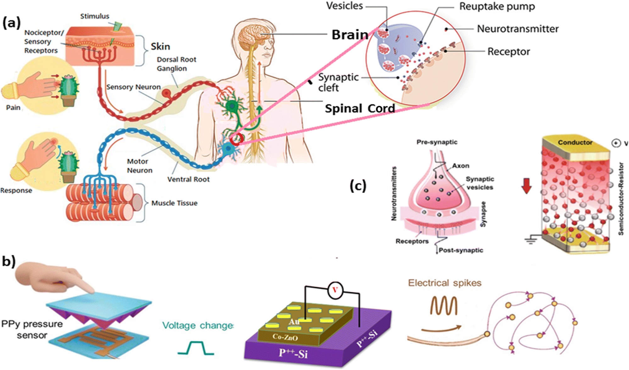 | ||
| Fig. 1 (a) A distinct nerve system and a biological tactile receptor are shown schematically. Transmission of mechanical signal to the brain via synapses and neurons as a result of external applied stress. The bio-synapse is sketched in the middle (enlarged). (b) Diagrammatic representation of the suggested artificial touch perception neuron. (c) Typical schematic illustration of the biological synapse (natural) and the self-doping memristors (artificial counterpart). | ||
Our CZO memristor-based nociceptors' threshold voltage keeps an eye on the electric field that traps injected electrons. Assume that there is not enough electrical input bias. Since the memristor will maintain its initial HRS and no output current will be observed, the external stimulation is therefore safe. Furthermore, the threshold value of nociceptor neuron is achieved if the stimulus intensity rises. Next, the memristor turns ON (LRS) when an output terminal current pulse is detected, suggesting that the external stimulation may be hazardous.
2 Experimental section
2.1 Film deposition
By depositing a 100 nm CZO thin film on a P++-Si substrate (resistivity 0.002–0.006 cm) using ZnO and Co targets on position A and B in a magnetron RF sputtering chamber (AC source for the ZnO target and DC source for the Co target), a device with the structural formula P++-Si/CZO/Au was created. At 70 W, 5 mTorr, and 50 °C, respectively, the RF power, working pressure, and substrate temperature were maintained. The CZO was made more crystalline by performing an open environment annealing process at 500 °C for 30 min. The ratio of the flow rate of Ar to O gas during the magnetron RF sputtering was 40/5. First, the Au (50 nm) electrode layer was deposited by a thermal evaporator using Au wire, then the switching layer that is CZO, was deposited on the top of P++-Si but before that, the P++-Si/CZO sample was covered by a metal mask with a pattern of a circular array. In order to finish off the device structure, the 50 nm Au layer was placed on top of the CZO layer. The same manufacturing procedure and environmental conditions were employed to create the P++-Si/ZnO/Au device.2.2 Device characterization
An X-ray diffractometer was used to take X-ray diffraction data. Using a scanning electron microscope (SEM, SM-7001F, JEOL), images of the P++-Si/CZO/Au (bottom) memristors in cross-section and from above were captured. The oxygen chemical states of CZO were assessed by X-ray photoelectron spectroscopy (XPS) (Thermo-VG Scientific ESCA Lab) 250. A source meter system (Keithley 2612B) was used to obtain all of the room-temperature and high-temperature I–V characteristics, reading voltages of 3, 8, 10, and 15 V under dark and light circumstances, respectively. An aluminum hot plate with changeable temperature was employed for temperature-dependent I–V characterization. The ambient conditions were used for all of the measurements.3 Results and discussion
3.1 Structure of the diffusive memristor
A diagrammatic representation of the proposed memristor is shown in Fig. 2a. It has a CZO layer packed in between a top electrode of Au and a bottom electrode of P++-Si. The experimental part contains more detailed information on the design and characterization of devices. The crystallinity of the CZO film was examined using X-ray diffraction (XRD), and the spectrum is displayed in Fig. 2b. According to data card JCPDS card no. 89–0510 and the literature, the diffracted peaks of CZO at 31.95°, 34.64°, 36.50°, and 56.72° reflect the (100), (002), (101), and (110) planes of the wurtzite-structure.45,46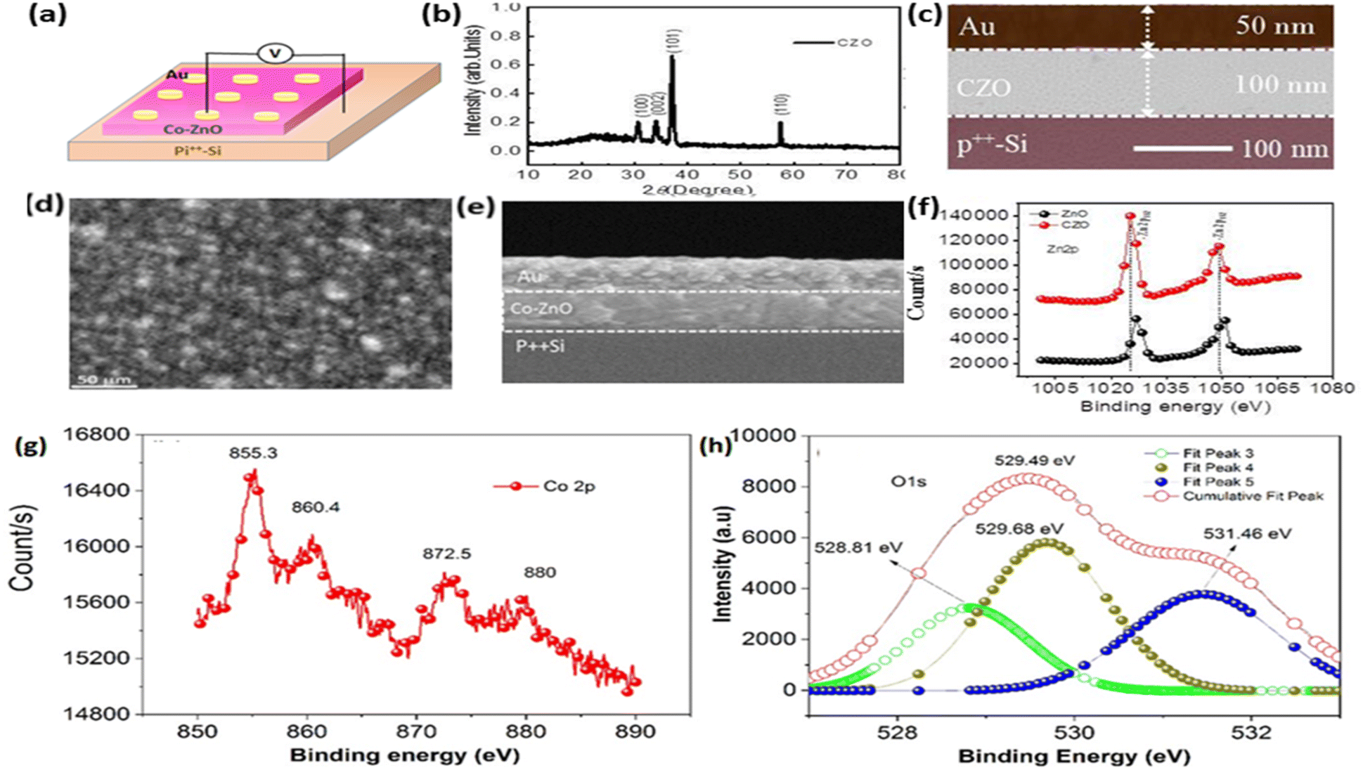 | ||
| Fig. 2 Schematic diagram and characterization of the structural response: (a) schematic of the three-dimensional structure, (b) X-ray diffraction pattern, (c) TEM cross-section picture, (d) surface electron microscopy picture, (e) cross-sectional SEM view, (f) 2p XPS spectrum of CZO and un-doped ZnO devices. (g) XPS spectrum of Co 2p, (h) XPS spectrum of O 1s. | ||
To confirm the device assembly and the constituent's makeup of the deposited films, we used SEM and TEM mapping to investigate the dimensional analysis of the P++-Si/CZO/Au device. The thickness of the Au TE is roughly 50 nm, and a 100 nm CZO film is well formed on a substrate, according to the 100 nm scale bar in the SEM and TEM images in Fig. 2c–e. From XPS survey spectra the only identified constituents are, Zn, O, and Co, indicating the purity of the CZO layer deposited by RF sputtering. Fig. 2f shows Zn 2p3/2 and Zn 2p1/2 of the ZnO thin film located at 1026.76 and 1049.58 eV, which indicates that Zn is in the divalent oxidation state.47 Furthermore, take note that the Zn 2p3/2 and Zn 2p1/2 peak positions were found to differ by 23.2 eV, which closely matches the ZnO characteristic value.48 As seen in Fig. 2f, the inclusion of Co2+ ions in the CZO film causes the Zn 2p3/2 and Zn 2p1/2 peaks of CZO to shift slightly toward lower binding energy when compared to pure ZnO. This result indicates that Co ions have replaced Zn sites in these thin films, as the majority of the Co ions are in the Co2+ state.49
The O 1s spectrum is shown in Fig. 2h, with peaks at 528.81, 529.68, and 531.46 eV. The OL ions bonding in the ZnO wurtzite structure and the OV ions in the oxygen-deficient areas (oxygen vacancy defects), are responsible for the peaks at 528.81 eV and 529.68 eV, respectively. The procedures of ZnO growth and annealing introduce the oxygen vacancy flaws. The peak at 531.46 eV can be attributed to chemisorbed oxygen,50,51 i.e., oxygen molecules in the air chemisorb on the surfaces of the ZnO thin layer and grab any free electrons in the n-type ZnO conduction band before converting them to oxygen ions,52 as presented in the reaction (1):
| O2(g) + e− → O2(ad) | (1) |
Four peaks can be identified in the Co 2p spectra of CZO given in Fig. 2g at the respective energies of 855.3, 860.4, 872.5, and 880.0 eV. The 20.4 eV energy difference between the peaks of Co 2p3/2 (860.4 eV) and Co 2p1/2 (800.0 eV) is what causes Co to be in the 2+ valence state.42 The presence of the satellite peak also shows that high-spin divalent Co2+ is present in the film but that no impurities were produced because the Co ion was substituted at the Zn location. The CZO sample contains more O2 species than pure ZnO because it has a higher donor fraction. Consequently, the presence of several oxygen vacancies changed the surface of the CZO sample.
3.2 I–V characteristics and conduction mechanism study
The CZO device's current–voltage (I–V) curves for a deposition area of 100 nm with continuous positive and negative voltage bias are shown in Fig. 3a and b in normal and semi-logarithmic scales. To protect the devices against long-term disruption, a compliance current of 13 mA was utilized together with the bias voltage sequence of 0 V → 15 V → −15 V → 0 V (dual sweep). The absence of any forming processes in the CZO devices may have been caused by the pre-existing VO in the thin films that had just been deposited. Fig. 3a shows a symmetrical hysteresis curve, which suggests resistive switching behavior. The device is initially in a highly resistive state with currents in the nA range when the voltage is less than 5 V. An insulating condition (HRS) transforms into a voltage-dependent low resistive state (LRS) at higher voltages, where the current reaction increases quickly as the voltage rises. The current spontaneously relax to its baseline value when the voltage is swept back from 15 V. As a result, unlike memristive devices, which frequently exhibit zero-crossing behaviour, the I–V sweeping of the CZO device does not reach zero. This feature sets this threshold switch device apart from others completely. Other threshold switch devices experience a sudden transition between resistance states due to conductive path formation and rupture, which results in a memory behaviour with zero-crossing characteristics.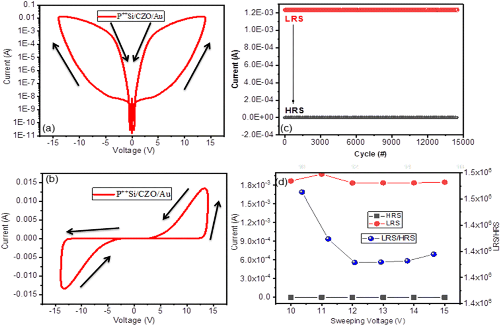 | ||
Fig. 3 The electrical characterization of fabricated memristor device (a) plotting of the sweeping performance at 15 V at a steady 0.1 V s−1 sweeping rate on a linear scale (b) plotting I–V curves on a semi-logarithmic scale (c) performance endurance (LHS/RHS) for device at reading voltage 3 V over 15![[thin space (1/6-em)]](https://www.rsc.org/images/entities/char_2009.gif) 000 sweeping cycles (d) LHS/RHS at different sweeping voltages. 000 sweeping cycles (d) LHS/RHS at different sweeping voltages. | ||
Additionally, for the range of reverse sweeping voltage, the devices exhibit symmetrical activity, suggesting threshold-switching action in both directions. The VO helped the CFs form quickly, which allowed the BRS characteristic to be seen in the CZO device even in the absence of a forming process. The CZO device has set and reset voltages of 1.22 and −1.01 V were seen in Fig. 3b, which showed our device's resistive, respectively. Hysteresis loops in the I–V curves switching characteristic. This trait differs noticeably from the non-volatile trait shown in the well-studied CMOS film sandwich between Pt-electrode devices, which exhibits threshold-switching behavior at lower sweeping bias and maintains its resistance states.2,53–55 The ZnO layer sandwiched between the Pt electrodes, where a bipolar nonvolatile resistive switching performance is commonly seen, is likewise different from this.56
The results in Fig. 3a demonstrated a rectifier's normal symmetrical property, which demonstrated that the positive current branch and the negative current branch are identical. The CZO device's capacitive characteristic transforms into a capacitive-coupled memristor characteristic at higher voltages. This phenomenon has already been documented in metal-oxide-based nonvolatile memory (NVM) devices.57 With different annealing temperatures but the same sputtering deposition parameters, an undoped ZnO-based P++-Si/ZnO/Au (100 nm) device was also synthesized. The memristive behaviour of P++-Si/ZnO/Au devices on a semilogarithmic scale reveals minimal variation in resistance states under voltage sweeping, with high conductivity being the main feature, as illustrated in Fig. S-2 (a–f).† The results of the endurance measurement are shown in Fig. 3c, At a read voltage of 3 V, the resistance in the HRS and LRS was measured. For over 15000 repetitive cycles, the HRS and LRS can be sustained, and the RS ratio can be maintained up to 103, indicating good stability and repeatability of the CZO device. As indicated in Fig. 3d, the LRS/HRS ratio depends on the sweeping voltage, this opens the door to employing the applied electric field to accurately control the resistance state. It was observed the I–V curve shows non-zero crossing. The observed non-zero crossing in the I–V curve of the Au/Co–ZnO/P++Si memristor, as highlighted in Fig. 3a and elaborated upon in the enlarged part of Fig. S3,† suggests a complex interplay between resistive switching mechanisms and capacitive effects.58 This behavior indicates dynamic charge redistribution within the device under different voltage biases. The capacitive coupling between the Co–ZnO layer and the electrodes (Au bottom electrode and P++Si substrate) likely contributes to the observed phenomenon, influencing charge dynamics and resistance switching characteristics. Understanding this interplay is crucial for elucidating the device's behavior and exploring its potential applications in emerging technologies.
Since conduction processes are often temperature dependent in different ways, plotting the conduction current against temperature delivers highly important information on the structure of the conduction currents. With a 10 mA compliance current, the temperature dependency of the I–V curves in insulating and conducting states at temperatures between 298 and 368 K is shown in Fig. 4a. To study the charge transport mechanism of the CZO device, As illustrated in Fig. 4a–f, we assessed the temperature-dependent I–V sweeping performance and separated the current response into four phases in the forward sweeping range. According to Fig. 4a, the current reaction considerably upsurges as temperature rises, pointing to a temperature-dependent charge transfer process in CZO device. The essential equations defining the charge transport process at different phases divided by the threshold voltage are fitted to the current under forward bias as a result of the symmetrical response. The behavior of the current in phase-I below the threshold voltage is shown in Fig. 4b; the linear slope of ln(J/T2) with 1/T denotes the emergence of a Schottky barrier. This is consistent with the theory that the Schottky interaction barrier is formed by the electrodes and CZO layer. The standardized Schottky emission model as mentioned in eqn (2) is depicted below:
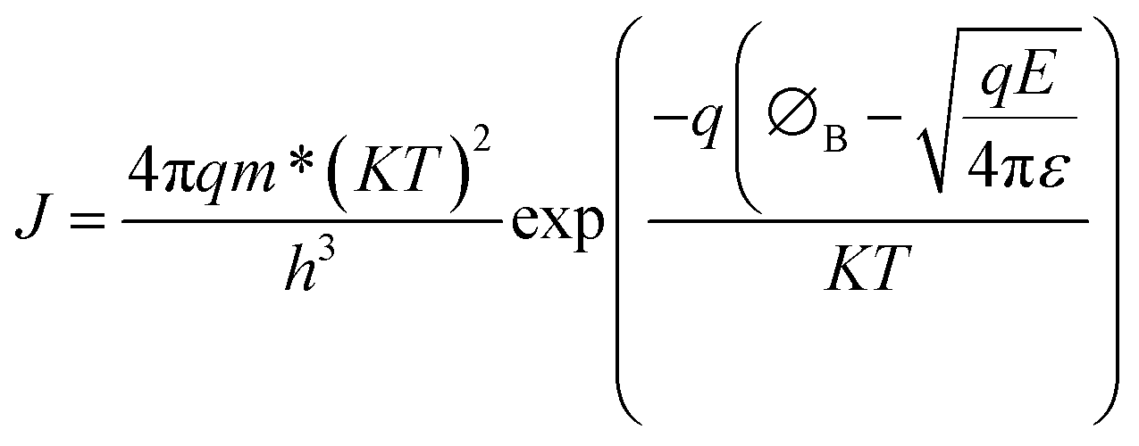 | (2) |
 | (3) |
 | (4) |
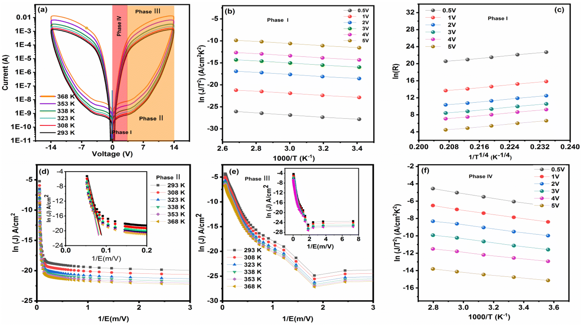 | ||
| Fig. 4 A CZO device's charge transport mechanism: (a) performance of sweeping depending on temperature between 293 and 368 K. For every measurement, a consistent sweeping rate of 0.1 V s−1 is employed. For fitting with various equations, four steps related to applying a bias are highlighted. (b) The relationship between inverse temperature (1/T) and ln(J/T2) For voltages in phase I. (c) The relationship between temperature (T−1/4) and ln(R) at various phase I low voltages. (d) The relationship between ln(J) and inverse electric field (1/E) at various temperatures for voltages in phase II. (e) The relationship between ln(J) and inverse electric field (1/E) at various temperatures for voltages in phase III. (f) The relationship between inverse temperature (1/T) and ln(J/T2) for voltages in phase IV. At each temperature, five sweeping cycles were recorded, and the corresponding average values and standard deviations were computed. | ||
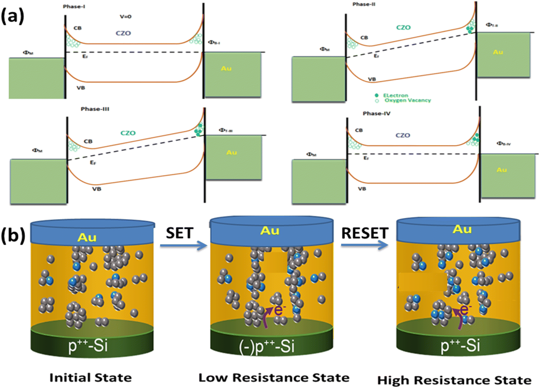 | ||
| Fig. 5 (a) Representation of mechanism I in the form of band diagram and (b) the resistive switching mechanism of CZO/Au in various phases. | ||
In phase I, Schottky emission dominates charge transport due to the realization of the electrons expected at many nearby trap locations in the small forward biasing (schematic Fig. 5). When the electrode is forward biased with high external voltage, the trap locations starts to be occupied by injected electrons from the Au electrode, to lower the Fermi level of the trap level. The defect-facilitated TAT behavior in Fig. 5a phase II is influenced by the trap states that are present at the Au/CZO interface. Dynamic electron trapping causes the trap-assisted tunneling phase to modulate, which causes hysteresis in phase III (phase II of Fig. 5a). When the effective Schottky barrier in phase IV decreases as a result of trapped electron accumulation under the applied electric field, spontaneous charge detrapping takes place, restoring the device to its starting condition (Fig. 5a phase IV). Shallow flaws on the CZO layer serve as a conductive transport channel throughout the procedure. An analogous method of charge transfer is obviously anticipated on both electrodes given the device's symmetrical energy band structure, which results in the experimental symmetrical I–V sweeping behavior.62,64
A similar RS mechanism is also shown in Fig. 5b to help understand the switching process in freestanding ZnO-based memristor devices. The behavior of Au in ZnO-based cells may be characterized using electrochemical processes (migration and buildup of Au ions and Au atoms) across bipolar electrodes, as has already described.65 In contrast, CZO-based memristor devices have a smaller bandgap (∼3.45 eV) and a greater dielectric constant (∼8.17), resulting in a stronger electric field within the CZO layer along with more Au atoms dissolving in the switching layer.66 ZnO limited ion mobility and redox reaction rate limit the movement and aggregation of Au atoms and Au ions across the interfacial layer.57 These two facts may result in the creation of a nano-cone-shaped filament from TE to BE. The concentrated metallic area in the shape of efficient containment of filament development in the shape of a nano-cone from TE to BE can provide control over resistance states during cyclic operation. When the top Au electrode is sufficiently positive biased across the double layers, the electric field across the dielectric layers is enough to move the Au ions from the Au TE to p++-Si BE through the interfacial layer, resulting in a reduction in the actual gap between electrodes (Fig. 5b). The Au-filaments do not disintegrate unless a negative voltage is provided, and they retain their initial state even when the bias voltage is withdrawn. When a negative voltage is provided, a typical RESET occurs, and Au CFs are partially desolated (generally at the thinnest point) as a result of the thermal-assisted electrochemical process.67 The memristor device turns off and returns to HRS (final panel of Fig. 5b), before cycling reversibly between two states (Fig. 5b) as a memristor device. The left panel of Fig. 5b illustrates that the filaments formed in this study are expected to possess greater thickness compared to those depicted in the center panel of the same figure. The latter filaments exhibit resistance to dissolution and rupture unless subjected to a negative voltage. Notably, the filaments within the CZO layer maintain a notably thinner profile, resembling a nano-cone structure. Consequently, the application of a negative bias leads to rapid filament rupture, as depicted in Fig. 5b. Moreover, with further voltage increment and subsequent current rise, there is a discernible risk of negative-SET occurrence within a high bias range, attributed to the presence of residual Au atoms near the surface of the BE.
3.3 The memristive nociceptor's pulse response
By measuring the diffusive memristor's pulses, the experimental demonstration of the three key characteristics of a normal nociceptor (undamaged case), namely “threshold,” “no adaptation,” and “relaxation,” was carried out. A natural nociceptor's triggering mechanism is strongly influenced by the strength, period, and magnitude of the motivations.68,69 To simulate external stimuli for our P++-Si/CZO/Au device, we used electrical surges of varied intensities, pulse widths, and pulse counts, as illustrated in Fig. 6. A train with fixed pulse amplitudes (15 V) and various pulse widths with time intervals of 10 ms was used to research the impact of pulse width on the device's response. We found that a 20 ms pulse width was sufficient to activate the nociceptor, and increasing the width to 100 ms resulted in a higher output current, as shown in Fig. 6a. It was discovered that the initial current jump took place after some time. This is consistent with a biological nociceptor's rise in response intensity rising with noxious stimulus intensity. Only voltage pulses of 2 V (50 ms width) for a train of electrical pulses with different amplitudes could activate the memristive nociceptor, However, as seen in Fig. 6b, the threshold value was not achieved until the pulse reached 5 V per 50 ms at a time interval of 10 ms. A memristive nociceptor's threshold for a noxious stimulus was determined by increasing the amplitude to 15 V (50 ms breadth, 10 ms time interval), which produced a bigger output current in line with the intensifying reaction. A higher voltage of 11 V is required for the device to initiate the current and the output current for device steadily increases, indicating a selective response to their triggered amplitude range Fig. 6b. This again displays how the voltage amplitude affects the device's threshold property. The fact that a 100 ms long pulse width was used during these single-pulse tests to provide the equipment enough time to return to its resting state between measurements is crucial. The number of electrical pulses the memristive nociceptor has already received determines how it will react to a series of pulses. Schematics Fig. 6c–e depict a train of 8, 10 and 15 V pulses of 50 ms pulse width and a series of pulses with 10 V amplitude and of varying widths (25 and 100 ms), together with the corresponding output current pulses (in the same graph). We found that the device could only be turned on with a sufficiently long pulse width (1 ms in this case) and a fixed pulse amplitude (15 V). A longer pulse also increased the output current. It was discovered that the initial current jump took place after some time Fig. 6a's inset. The response of the device to an electrical pulse train depends significantly on how many pulses it receives. Additionally, it suggests that more pulses are needed to turn on the device if the amplitude is lower. The creation of conducting routes within the switching layer is responsible for the “threshold” quality shown with the memristive nociceptor, which is in line with what has been demonstrated in its anatomical equivalent. These top-to-bottom electrode-bridging pathways need to be generated with enough amplitude and duration.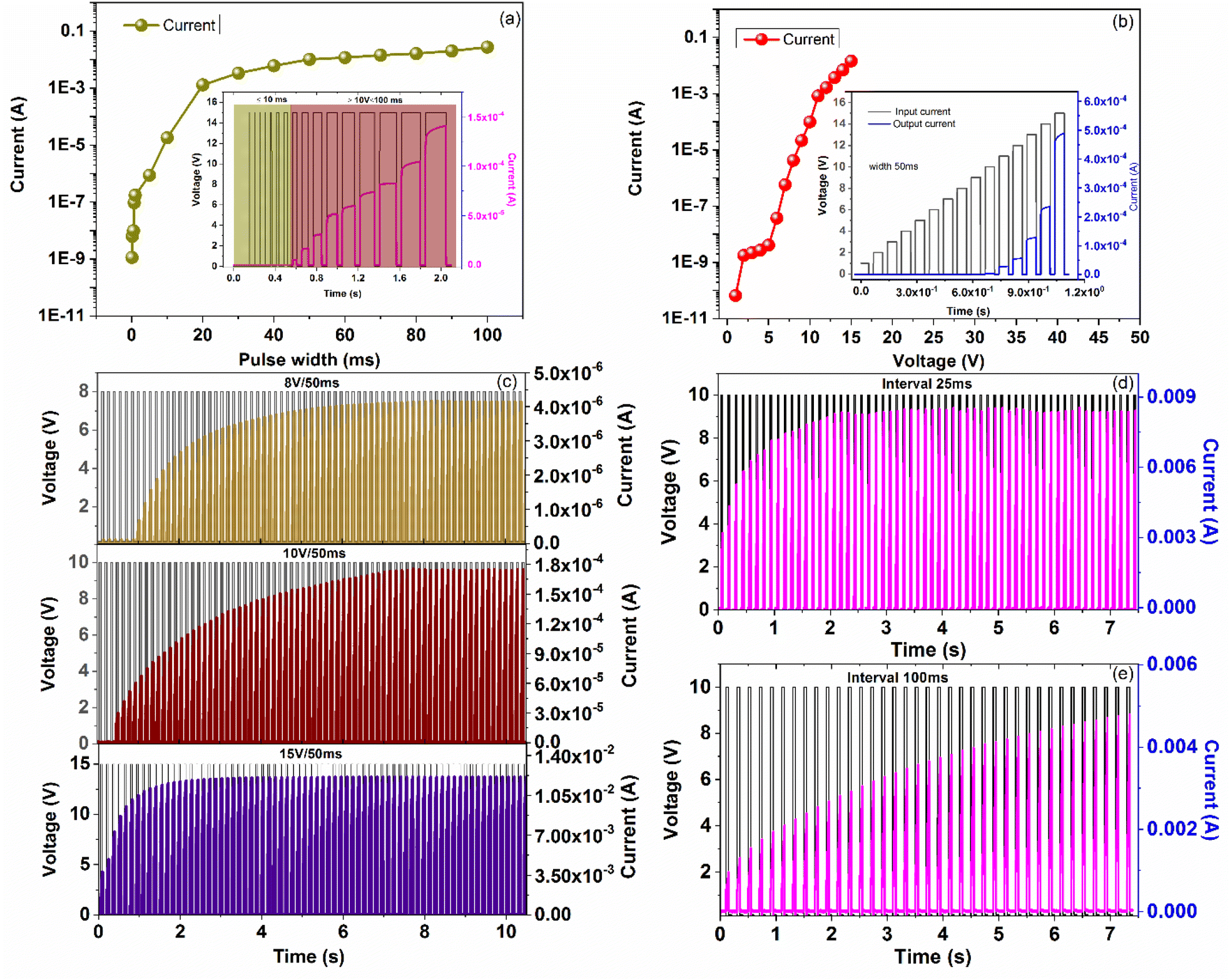 | ||
| Fig. 6 Nociceptive behavior. (a) Corresponding output current at different pulse width. A succession of voltage pulses with amplitude 15 V (dark yellow curve) of different pulse lengths (1 ms to 100 ms) with interval 10 ms and the corresponding output currents (pink curve) [inset]. (b) Corresponding output current at different applied voltages. The output currents that correspond to a sequence of various voltage with a pulse width of 50 ms (black curve; 1.0 to 15 V, time interval 10 ms) are shown in the blue curve. An increased output current is caused by a greater input voltage [inset] (c). The devices achieve the saturation state after a series of 50 ms, 8, 10, and 15 V pulses are delivered; there is no adaptation response. (d and e) Pulse response of memristors with intervals of 25 ms and 100 ms with amplitude of 10 V. The adaptation rate of rapidly and slowly respectively. | ||
Following each applied pulse, the current generation progressively rises, indicating that the electrons inserted by the pulsations are progressively occupying the empty trap levels and allowing more steady conduction for succeeding pulses.
Moreover, it was noted that the current increased up to the saturated point, suggesting that the current devices could be used to mimic the “no adaptation” characteristic of nociceptors, in which a neuron does not adjust to more repeated unpleasant biasing because the sensitivity of the nociceptor slowly decreases with prolonged contact to outside stimuli.68 The human body must experience these phenomena, which is analogous to the nociceptor's “no adaptation” characteristic, in order to defend itself from repeated damaging shocks.
3.4 Sensitization function in a memristive nociceptor
A nociceptor is said to be injured when it is subjected to strong enough stimuli to cause damage. Following injury, a nociceptor will exhibit an enhanced response at a lower threshold, which is referred to as “hyperalgesia” and “allodynia”.68–70 This is illustrated schematically in Fig. 7a. We initially applied the high value pulses of 0 V, 5 V, 10 V, and 15 V with a pulse width of 20 ms, creating a modification that imitates the injury or damage to the nociceptor device in order to illustrate the “sensitization” property of a P++-Si/CZO/Au memristive nociceptor. We evaluated our device's current response to different input stimuli, as shown in Fig. 7b, to see if it had sustained different levels of “damage.” It is evident from Fig. 7c and d that the “injured” nociceptors have a larger output current and that the input voltage affects their maximum output current. Interestingly, when the output current rose, the threshold voltage moved towards the lower value. This shows that a lower threshold voltage is desired to activate more gravely damaged devices in order to recreate allodynia and hyperalgesia in the nociceptor. The behaviour of the threshold shift has been validated by many series of pulse tests, as Fig. 7d illustrates. Further evidence of how the device's threshold alters with the high voltage pulse, comes from the fact that the figure of pulses necessary to switch on the device is significantly lower and the generation current is significantly greater in an injured situation (after five 10 V pulses). This phenomenon is linked to the nociceptors' apparent key characteristic—their great sensitivity during the relaxation period. Nociceptor protection is the process by which nociceptors react to pre-injury stimuli and then more rapidly and accurately identify stimuli that may be harmful.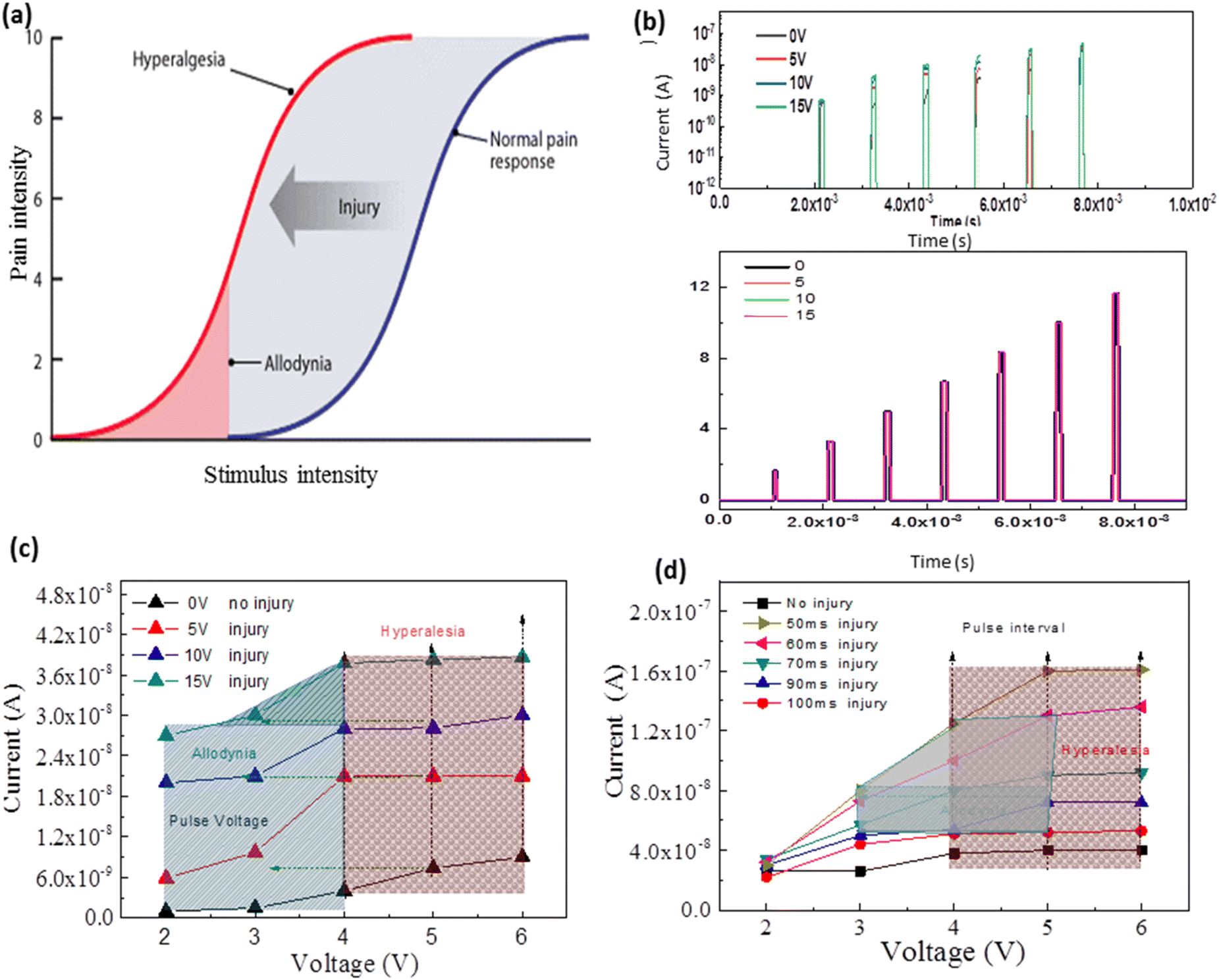 | ||
| Fig. 7 A memristive's nociceptive behaviour (a) schematic illustration showing the characteristics of hyperalgesia and allodynia in response to increased stimuli intensity in both damaged (injury) and normal pain circumstances. (b) A series of pulses with an amplitude ranging from 2 to 7 V in the input voltage. The nociceptor was exposed to the following pulses, each with a 2 ms pulse width: 0 V, 5 V, 10 V, and 15 V (2 ms) (such as in an injury occurrence). The output current that matches. (c) The current response showed signs of both allodynia and hyperalgesia for a series of pulses from 2 to 6 V (20 ms) after high-amplitude pulses (10 and 15 V pulse, 20 ms) were stimulated. (d) The reaction of the current to a series of pulses from 2 to 6 V (20 ms) showed both hyperalgesia and allodynia features when different pulses (0 V, 5 V, 10 V, and 15 V 20 ms pulse) with variable time intervals were stimulated. | ||
4 Conclusions
We have demonstrated improved memristive behavior CZO system, it is also used in neuromorphic computing to emulate synaptic response. In response to a quantum tunnelling with defect assistance process at high voltage and a Schottky partial process at low voltage, current flows in the CZO device. At different stages, there is also active charge trapping and detrapping with surface trap energy levels. Therefore, surface imperfections that contribute to the CZO device's high conductivity can be reduced. Additionally, at low electric fields, the imperfections in the layer between surfaces offer localized trap locations for electron skipping, and at high electric fields, they facilitate the tunnelling of electrons through the barrier and into the ZnO nanowire's conduction band. Based on analogue and digital switching characteristics, the relative resistive switching behavior of the devices was examined by evaluating the I–V characteristics and installing conduction models. Future useful memory device applications can be expanded thanks to this device study. The result is a voltage-dependent threshold switching performance that can be used to simulate every important characteristic of a nociceptor, such as “hyperalgesia,” “relaxation,” “no adaptation,” and “threshold.”Author contributions
Naveed Ur Rahman, Aziz Ullah, Muhammad Adil Mahmood, Nasir Rahman, Rajwali Khan: performed the experiment and wrote the original paper. Mohammad Sohail, Shahid Iqbal, Nizomiddin Juraev, Khaled Althubeiti, Sattam Al Otaibi, Rajwali Khan: discussed the results and implications. Naveed Ur Rahman and Rajwali Khan performed and analyzed the XRD spectrum. All authors commented on and approved the final version of the manuscript. Finally, Sattam Al Otaibi has successfully helped and guides us in comments addressing and removing grammatical errors.Conflicts of interest
The authors declare no interest conflict. They have no known competing financial interests or personal relationships that could have appeared to influence the work reported in this paper.Acknowledgements
The authors extend their appreciation to Taif University, Saudi Arabia, for supporting this work through project number (TU-DSPP-2024-59).References
- G. Atwood, Future directions and challenges for ETox flash memory scaling, IEEE Trans. Device Mater. Reliab., 2004, 4(3), 301–305 Search PubMed.
- D. B. Strukov, et al., The missing memristor found, Nature, 2008, 453(7191), 80–83 CrossRef CAS PubMed.
- A. Chen, A review of emerging non-volatile memory (NVM) technologies and applications, Solid-State Electron., 2016, 125, 25–38 CrossRef CAS.
- C.-C. Shih, et al., Ultra-low switching voltage induced by inserting SiO 2 layer in indium–tin–oxide-based resistance random access memory, IEEE Electron Device Lett., 2016, 37(10), 1276–1279 CAS.
- Y.-S. Fan, P.-T. Liu and C.-H. Hsu, Investigation on amorphous InGaZnO based resistive switching memory with low-power, high-speed, high reliability, Thin Solid Films, 2013, 549, 54–58 CrossRef CAS.
- M. Zackriya, H. M. Kittur and A. Chin, A novel read scheme for large size one-resistor resistive random access memory array, Sci. Rep., 2017, 7(1), 42375 Search PubMed.
- R. Ge, et al., Atomristor: nonvolatile resistance switching in atomic sheets of transition metal dichalcogenides, Nano Lett., 2018, 18(1), 434–441 CrossRef CAS PubMed.
- J. Borghetti, et al., Memristive’switches enable ‘stateful’logic operations via material implication, Nature, 2010, 464(7290), 873–876 Search PubMed.
- S. S. More, et al., Resistive switching and synaptic properties modifications in gallium-doped zinc oxide memristive devices, Results Phys., 2019, 12, 1946–1955 CrossRef.
- A. V. Pawar, et al., MemSens: a new detection method for heavy metals based on silver nanoparticle assisted memristive switching principle, J. Mater. Sci.: Mater. Electron., 2019, 30, 11383–11394 CrossRef CAS.
- A. Hao, et al., Ce-doping induced enhancement of resistive switching performance of Pt/NiFe2O4/Pt memory devices, Ceram. Int., 2017, 43, S481–S487 CrossRef CAS.
- A. Goossens, A. Das and T. Banerjee, Electric field driven memristive behavior at the Schottky interface of Nb-doped SrTiO3, J. Appl. Phys., 2018, 124(15), 152102 CrossRef.
- X. Song, et al., Effects of pyrazine derivatives and substituted positions on the photoelectric properties and electromemory performance of D–A–D series compounds, Materials, 2018, 11(10), 2063 CrossRef PubMed.
- J. Guo, et al., Enhanced magnetic modulation in HfO2-based resistive memory with an Hf top electrode, Appl. Phys. Lett., 2018, 113(4), 043502 CrossRef.
- J. Jang, et al., Highly improved switching properties in flexible aluminum oxide resistive memories based on a multilayer device structure, Adv. Electron. Mater., 2018, 4(12), 1800355 Search PubMed.
- N. Elboughdiri, et al., Enhanced electrical and magnetic properties of (Co, Yb) co-doped ZnO memristor for neuromorphic computing, RSC Adv., 2023, 13(51), 35993–36008 RSC.
- X. Yan, et al., Memristor with Ag-cluster-doped TiO2 films as artificial synapse for neuroinspired computing, Adv. Funct. Mater., 2018, 28(1), 1705320 CrossRef.
- S. Porro, et al., A multi-level memristor based on atomic layer deposition of iron oxide, Nanotechnology, 2018, 29(49), 495201 Search PubMed.
- F. Miao, et al., Anatomy of a nanoscale conduction channel reveals the mechanism of a high-performance memristor, Adv. Mater., 2011, 23(47), 5633–5640 Search PubMed.
- Ü. Özgür, et al., A comprehensive review of ZnO materials and devices, J. Appl. Phys., 2005, 98(4), 11 Search PubMed.
- N. Xu, et al., Bipolar switching behavior in TiN/ZnO/Pt resistive nonvolatile memory with fast switching and long retention, Semicond. Sci. Technol., 2008, 23(7), 075019 CrossRef.
- S. Kim, et al., Resistive switching characteristics of sol–gel zinc oxide films for flexible memory applications, IEEE Trans. Electron Devices, 2009, 56(4), 696–699 CAS.
- J. Won Seo, et al., Transparent flexible resistive random access memory fabricated at room temperature, Appl. Phys. Lett., 2009, 95(13), 133508 CrossRef.
- G. Hassan, et al., Resistive switching device based on water and zinc oxide heterojunction for soft memory applications, Mater. Sci. Eng. B, 2019, 246, 1–6 CrossRef CAS.
- M. Janousch, et al., Role of oxygen vacancies in Cr-doped SrTiO3 for resistance-change memory, Adv. Mater., 2007, 19(17), 2232–2235 CrossRef CAS.
- H.-W. Huang, et al., Stability scheme of ZnO-thin film resistive switching memory: influence of defects by controllable oxygen pressure ratio, Nanoscale Res. Lett., 2013, 8, 1–7 CrossRef CAS PubMed.
- H. Li, et al., Resistive switching characteristics of ZnO based ReRAMs with different annealing temperatures, Solid-State Electron., 2012, 75, 28–32 CrossRef CAS.
- F. M. Simanjuntak, et al., Status and prospects of ZnO-based resistive switching memory devices, Nanoscale Res. Lett., 2016, 11, 1–31 CrossRef CAS PubMed.
- H. Xu, et al., Effect of Co doping on unipolar resistance switching in Pt/Co: ZnO/Pt structures, J. Alloys Compd., 2016, 658, 806–812 CrossRef CAS.
- A. Younis, D. Chu and S. Li, Bi-stable resistive switching characteristics in Ti-doped ZnO thin films, Nanoscale Res. Lett., 2013, 8, 1–6 CrossRef PubMed.
- D. L. Xu, et al., Bipolar resistive switching behaviors in Cr-doped ZnO films, Microelectron. Eng., 2014, 116, 22–25 CrossRef CAS.
- C. Chappert, A. Fert and F. N. Van Dau, The emergence of spin electronics in data storage, Nat. Mater., 2007, 6(11), 813–823 CrossRef CAS PubMed.
- A. Kumar and M. Baghini, Experimental study for selection of electrode material for ZnO-based memristors, Electron. Lett., 2014, 50(21), 1547–1549 CrossRef CAS.
- W. Xue, et al., Intrinsic and interfacial effect of electrode metals on the resistive switching behaviors of zinc oxide films, Nanotechnology, 2014, 25(42), 425204 Search PubMed.
- R. Khan, et al., Resistive Switching Properties in Memristors for Optoelectronic Synaptic Memristors: Deposition Techniques, Key Performance Parameters, and Applications, ACS Appl. Electron. Mater., 2023, 6(1), 73–119 CrossRef.
- G. Milano, et al., Structure-Dependent Influence of Moisture on Resistive Switching Behavior of ZnO Thin Films, Adv. Mater. Interfaces, 2021, 8(16), 2100915 CrossRef CAS.
- S. Dayanidhi and F. J. Valero-Cuevas, Dexterous manipulation is poorer at older ages and is dissociated from decline of hand strength, J. Gerontol. A Biol. Sci. Med. Sci., 2014, 69(9), 1139–1145 CrossRef PubMed.
- H. A. Yanco, Wheelesley: A robotic wheelchair system: Indoor navigation and user interface, Assistive technology and artificial intelligence: applications in robotics, user interfaces and natural language processing, 2006, pp. 256–268 Search PubMed.
- G. Riegler, et al., High-resolution ultrasound visualization of Pacinian corpuscles, Ultrasound Med. Biol., 2018, 44(12), 2596–2601 CrossRef PubMed.
- J. Feito, et al., The development of human digital Meissner's and Pacinian corpuscles, Ann. Anat., 2018, 219, 8–24 CrossRef CAS PubMed.
- I. A. Khasabova, et al., Pioglitazone, a PPARγ agonist, reduces cisplatin-evoked neuropathic pain by protecting against oxidative stress, Pain, 2019, 160(3), 688–701 CrossRef CAS PubMed.
- E. E. Okuyucu, et al., Does transcutaneous nerve stimulation have effect on sympathetic skin response?, J. Clin. Neurosci., 2018, 47, 160–162 CrossRef PubMed.
- C.-L. Chen, et al., Runx1 determines nociceptive sensory neuron phenotype and is required for thermal and neuropathic pain, Neuron, 2006, 49(3), 365–377 CrossRef CAS PubMed.
- R. E. Brown, T. W. Bligh and J. F. Garden, The Hebb synapse before Hebb: theories of synaptic function in learning and memory before, with a discussion of the long-lost synaptic theory of William McDougall, Front. Behav. Neurosci., 2021, 15, 732195 CrossRef PubMed.
- J. Adeleke, et al., Photocatalytic degradation of methylene blue by ZnO/NiFe2O4 nanoparticles, Appl. Surf. Sci., 2018, 455, 195–200 CrossRef CAS.
- K.-M. Kang, et al., Study on properties of Ga/F-co-doped ZnO thin films prepared using atomic layer deposition, Thin Solid Films, 2018, 660, 913–919 CrossRef CAS.
- F.-M. Chang, et al., Strong correlation between optical properties and mechanism in deficiency of normalized self-assembly ZnO nanorods, Sci. Rep., 2019, 9(1), 905 CrossRef PubMed.
- T. Basu, et al., Thickness-dependent blue shift in the excitonic peak of conformally grown ZnO: Al on ion-beam fabricated self-organized Si ripples, J. Appl. Phys., 2015, 118(10), 104903 CrossRef.
- Y. Zhang, et al., Pulsed laser ablation of preferentially orientated ZnO: Co diluted magnetic semiconducting thin films on Si substrates, Appl. Phys. Lett., 2006, 89(4), 042510 Search PubMed.
- Y. Caglar, Sol–gel derived nanostructure undoped and cobalt doped ZnO: Structural, optical and electrical studies, J. Alloys Compd., 2013, 560, 181–188 CrossRef CAS.
- F. Zhuge, et al., Improvement of resistive switching in Cu/ZnO/Pt sandwiches by weakening the randomicity of the formation/rupture of Cu filaments, Nanotechnology, 2011, 22(27), 275204 CrossRef PubMed.
- P. Russo, et al., UV-Induced Multilevel Current Amplification Memory Effect in Zinc Oxide Rods Resistive Switching Devices, Adv. Funct. Mater., 2018, 28(13), 1706230 CrossRef.
- K. M. Kim, et al., A detailed understanding of the electronic bipolar resistance switching behavior in Pt/TiO2/Pt structure, Nanotechnology, 2011, 22(25), 254010 CrossRef PubMed.
- Y.-J. Huang, et al., Dual-functional memory and threshold resistive switching based on the push-pull mechanism of oxygen ions, Sci. Rep., 2016, 6(1), 23945 Search PubMed.
- J. J. Yang, et al., Memristive switching mechanism for metal/oxide/metal nanodevices, Nat. Nanotechnol., 2008, 3(7), 429–433 CrossRef CAS PubMed.
- C.-N. Peng, et al., Resistive switching of Au/ZnO/Au resistive memory: an in situ observation of conductive bridge formation, Nanoscale Res. Lett., 2012, 7, 1–6 CrossRef PubMed.
- R. Khan, et al., Threshold switching in nickel-doped zinc oxide based memristor for artificial sensory applications, Nanoscale, 2023, 15(4), 1900–1913 RSC.
- B. Sun, et al., Non–zero-crossing current-voltage hysteresis behavior in memristive system, Mater. Today Adv., 2020, 6, 100056 Search PubMed.
- Z. Chen, et al., Vertically aligned ZnO nanorod arrays sentisized with gold nanoparticles for Schottky barrier photovoltaic cells, J. Phys. Chem. C, 2009, 113(30), 13433–13437 CrossRef CAS.
- L. J. Brillson and Y. Lu, ZnO Schottky barriers and Ohmic contacts, J. Appl. Phys., 2011, 109(12) CrossRef CAS.
- Y. Hu, et al., Observation of a 2D Electron Gas and the Tuning of the Electrical Conductance of ZnO Nanowires by Controllable Surface Band-Bending, Adv. Funct. Mater., 2009, 19(15), 2380–2387 CrossRef CAS.
- M. Xiao, et al., Ultrathin TiOx Interface-Mediated ZnO-Nanowire Memristive Devices Emulating Synaptic Behaviors, Adv. Electron. Mater., 2019, 5(6), 1900142 CrossRef.
- E. W. Lim and R. Ismail, Conduction mechanism of valence change resistive switching memory: A survey, Electronics, 2015, 4(3), 586–613 CrossRef CAS.
- M. Xiao, et al., Threshold switching in single metal-oxide nanobelt devices emulating an artificial nociceptor, Adv. Electron. Mater., 2020, 6(1), 1900595 CrossRef CAS.
- T. Shi, et al., A review of resistive switching devices: performance improvement, characterization, and applications, Small Struct., 2021, 2(4), 2000109 CrossRef.
- J. Xu, et al., Surface engineering of ZnO nanostructures for semiconductor-sensitized solar cells, Adv. Mater., 2014, 26(31), 5337–5367 CrossRef CAS PubMed.
- Q. Liu, et al., Real-time observation on dynamic growth/dissolution of conductive filaments in oxide-electrolyte-based ReRAM, Adv. Mater., 2012, 24(14), 1844 Search PubMed.
- J. H. Yoon, et al., An artificial nociceptor based on a diffusive memristor, Nat. Commun., 2018, 9(1), 417 CrossRef PubMed.
- J. Ge, et al., Flexible artificial nociceptor using a biopolymer-based forming-free memristor, Nanoscale, 2019, 11(14), 6591–6601 RSC.
- Y. Kim, et al., Nociceptive memristor, Adv. Mater., 2018, 30(8), 1704320 CrossRef PubMed.
Footnote |
| † Electronic supplementary information (ESI) available. See DOI: https://doi.org/10.1039/d4ra01250j |
| This journal is © The Royal Society of Chemistry 2024 |