
 Open Access Article
 This Open Access Article is licensed under a Creative Commons Attribution-Non Commercial 3.0 Unported Licence
CuInS2 quantum dots-based unipolar resistive switching for non-volatile memory applications†
Harshit
Sharma
ab,
Nitish
Saini
ab,
Lalita
ab,
Divya
Kaushik
ab,
Ajeet
Kumar
 *ab and
Ritu
Srivastava
*ab
*ab and
Ritu
Srivastava
*ab
aAcademy of Scientific and Innovative Research (AcSIR), Ghaziabad 201002, India
bCSIR-National Physical Laboratory, Dr. KS Krishnan Marg, New Delhi 110012, India. E-mail: ritu@nplindia.org; kumarajeet@nplindia.org
First published on 7th May 2024
Abstract
Recent advancements have established quantum dots (QDs) as a promising alternative to conventional bulk materials in the fabrication of nanoscale integrated electronic devices. The appeal of QDs lies in their amenability to low-temperature processes and solution-based methodologies, facilitating the construction of devices with enhanced versatility and efficiency. The ternary metal chalcogenide CuInS2 QDs are one of the foremost, eco-friendly, and highly stable materials. In this study, CuInS2 QDs are employed as a functional layer in a memristive device featuring an Al/CuInS2/ITO configuration. The CuInS2 QDs have been synthesized by a hot injection method and characterized using X-ray diffraction (XRD) and transmission electron microscopy (TEM) to reveal their structural features. The Al/CuInS2/ITO device shows a unipolar resistive switching (RS) behaviour with a high on/off ratio of 105. The switching parameters have been studied for 100 cycles of SET/RESET. The SET and RESET voltages are found to be 1.66 ± 0.25 V and 0.69 ± 0.17 V. The spatial variability of switching parameters in the Al/CuInS2/ITO structure has also been studied for 9 different devices. The device also exhibits unipolar RS behaviour in the optimum temperature range of 0 °C to 50 °C. These outcomes demonstrate the impressive performance of CuInS2 QDs, indicating their potential for future energy-efficient and large-scale non-volatile memory applications.
1 Introduction
In recent times, the miniaturization potential of silicon-based complementary metal oxide semiconductor (CMOS) technology has reached saturation and it is leading to a surge in demand for new materials and technologies that can deliver smaller, faster, and more integrated memory units. Resistive switching random-access memory (RRAM) has emerged as an alternative to CMOS-based memory units for technological advancement.1 The electric field-driven interchangeable resistance states with faster interstate switching time and low power consumption makes it the most promising technology for futuristic devices.2–7 The structure of RRAM devices is marked by its simplicity, featuring a metal–insulator–metal (MIM) arrangement where a functional layer is placed between two metal electrodes. The characteristics of the functional layer embedded between two metal electrodes are crucial in influencing key parameters and directing the switching mechanisms in RRAM. Metal oxides have hitherto undergone extensive investigation as potential candidates for the functional layer in RRAM.8,9 Although metal oxides-based RRAM performed well as functional layer, they need high temperature treatment for fabrication. This limits their integration in mass-produced nanoscale electronics and flexible devices. Within the realm of RRAM devices, metal chalcogenides have emerged as viable candidates for deployment as functional layers.10–14 Solution-processable methodologies, coupled with low-temperature treatment for the formation of metal chalcogenides thin films, can address the imperative for scalable production and facilitate the realization of flexible devices. The electrochemically active metals like Ag and Cu-based chalcogenide materials demonstrated the RS phenomenon due to the redox behavior of the Ag and Cu ions15–17 and the lax bonding of metallic ions within these chalcogenides framework which promotes their migration under the influence of an applied electric field. With the same concept, ternary metal chalcogenides also show the RS behavior.15,18 As compared to the binary metal chalcogenides, the ternary metal chalcogenides are anticipated to exhibit enhanced properties through the incorporation of a third element, owing to the resulting stoichiometric variations and synergistic effects.19 In this aspect, ternary metal sulfide CuInS2 is a non-toxic and stable material which renders it a prospective candidate for the advancement of next-generation green electronics.20,21 CuInS2 QDs have been used for many optoelectronic applications such as solar cells, light-emitting diodes, photodetectors, etc.21–25 Recently, nanocomposites and nanosheets of CuInS2 have been investigated for RS behaviour, which exhibits a large switching window and low power consumption.26,27 Yun et al. utilized CuInS2 quantum dots (QDs) as nano-composites with graphene oxide to enhance device performance.27 T. Ahmad et al. employed magnetron sputtering for CuInS2 film deposition, demonstrating bipolar RS behavior; however, the requirement for high vacuum conditions during sputtering limits scalability for mass production.28 Additionally, Z. Hu et al. reported on a vertical aligned CuInS2 nanosheets array for bipolar RS behavior.26 Notably, Zhu et al. investigated the pristine CuInS2 QDs-based film for RS applications, revealing a Pt/CuInS2/Au structured device exhibiting bipolar RS behavior with high switching voltages of ±4.5 V.29In this study, a pristine CuInS2 QDs based solution processable thin film is investigated as a functional layer for novel Al/CuInS2/ITO structured RS devices. The facile synthesis of CuInS2 QDs, coupled with the subsequent fabrication of thin films employing solution-processable techniques and low-temperature treatment,30–32 renders the material amenable for the scalable production of devices. Moreover, employing pristine QDs films avoids the need for complex preparation methods associated with functional layers, such as the creation of nanocomposites, alignment of nanosheet arrays, and the use of vacuum-based techniques. Instead, it offers a straightforward, solution-processable approach to fabrication, thereby opening avenues for mass production. Here, a CuInS2 QDs-based functional layer was generated employing a spin-coating methodology to construct the devices. While previous studies focused solely on the bipolar RS behavior, the Al/CuInS2/ITO device shows a unipolar RS behavior marking the first investigation of unipolar RS behavior in CuInS2 based RS devices. The device exhibited remarkable performance characteristics, including low switching voltages below 2 V, a high on/off ratio of 105, and reproducible behavior. Additionally, both temporal and spatial variabilities in switching parameters were also studied which is an aspect not extensively examined previously. This investigation also included an analysis of the effect of working temperature on device performance, an essential consideration for real-world applications that has been overlooked in prior reports. Moreover, impedance spectroscopy has been performed for both the low resistance state (LRS) and high resistance state (HRS) of the device, and a reasonable switching mechanism model has been proposed. The findings underscore the potential of CuInS2 as a promising candidate for non-volatile memory devices.
2 Experimental
Copper(I) iodide, indium(III) acetate, oleic acid, and 1-octadecene were purchased from Sigma Aldrich. Dodecanethiol, acetone, and toluene were purchased from Alfa Aesar.The CuInS2 QDs were synthesised via the hot injection method as reported previously33,34 and a schematic of the synthesis is shown in Fig. S1 (ESI†). First, the copper iodide (464 mg), indium acetate (76 mg), dodecanethiol (1 ml), and 10 ml octadecene were mixed in a three-neck flask equipped with a water condenser under the continuous purging of argon (Ar) gas. The solution was continuously stirred at a temperature of 120 °C for 30 minutes. Then 0.5 ml of oleic acid was injected into the mixture and this was kept stirring at the same temperature. After 30 min, the temperature was increased to 210 °C and the mixture continued to be stirred for another 30 min until the solution was converted into a deep red colloidal solution. The colloidal solution underwent cooling to reach room temperature. Subsequently, to precipitate the CuInS2 QDs, acetone was introduced into the solution and then centrifuged at 5000 rpm for the collection of CuInS2 QDs. The solution was decanted, and the gathered QDs were re-dispersed in toluene. These were again precipitated by adding acetone and further collected by centrifuging at 5000 rpm. This dispersion underwent repeated precipitation by adding acetone, followed by collection through centrifugation at 5000 rpm. This purification procedure was iterated 2–3 times. Following purification, the CuInS2 QDs were re-dispersed in toluene, serving as a precursor for the CuInS2 film.
In the device fabrication process, the glass substrate coated with indium tin oxide (ITO) underwent ultrasonication treatment successively in DI water, acetone, and 2-propanol for 10 minutes each, followed by drying in a vacuum oven. After cleaning, the ITO substrate was spin-coated with the CuInS2 precursor at 1000 rpm for 30 seconds, followed by drying at 120 °C for 10 minutes. The top aluminum electrode was deposited using the thermal evaporation method under a vacuum pressure of 5 × 10⁻⁶ mbar. A shadow mask was employed to achieve a top electrode with dimensions of 200 × 200 µm2 during the deposition process. The memristor's measurements were recorded utilizing a two-probe setup with a Keithley-4200 source meter.
3 Results and discussion
The as-synthesised CuInS2 QDs have been characterized using X-ray diffraction (XRD) with a Cu Kα source (λ = 0.15418 nm) to reveal the phase and crystallographic structure. The deposited film of QDs on the glass substrate shows three major diffraction peaks as shown in Fig. 1(a) which can be indexed to the (112), (204), and (312) planes corresponding to the standard chalcopyrite phase of CuInS2 (JCPDS card file no. 75-0106). The wider diffraction peaks as observed imply the smaller size or poor crystallinity of the CuInS2 QDs.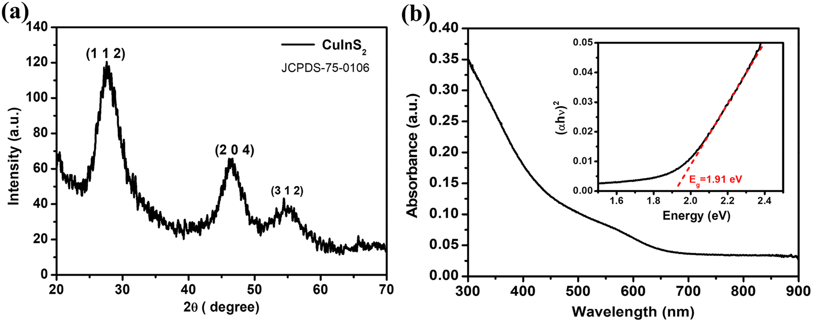 | ||
| Fig. 1 (a) XRD pattern of CuInS2 film, (b) UV-visible absorption spectrum of CuInS2 QDs. | ||
The UV-visible absorbance spectrum of the film is shown in Fig. 1(b) with the corresponding Tauc plot (inset). This shows a characteristic absorbance peak at 580 nm and by extrapolating the linear region in the Tauc plot the corresponding band gap is found to be 1.91 eV. This band gap differs from the bulk CuInS2 band gap which agrees with the quantum size of the material. The QDs have been characterized with high-resolution transmission electron microscopy (HRTEM) (Fig. 2(a) and (b)). The size of the QDs is found to be 1.9 ± 0.4 nm and the diffraction pattern shows an interplanar spacing of 0.32 nm which corresponds to the (112) crystallographic plane.
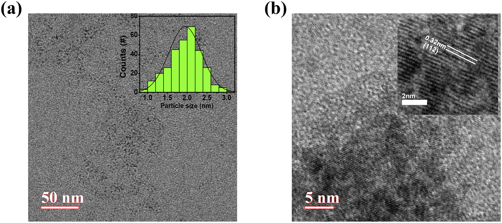 | ||
| Fig. 2 (a) HRTEM micrograph of CuInS2 QDs with size distribution (inset), (b) high-resolution HRTEM micrograph with fringes pattern (inset). | ||
The fabricated device structure, i.e. Al/CuInS2/ITO, as shown in Fig. 3(a), has been characterized for RS behaviour and Fig. 3(b) shows the 5 µm × 5 µm scale AFM micrograph of the CuInS2 film on ITO coated glass substrate. This shows a uniform film of CuInS2 on ITO with an RMS (root mean square) roughness of 0.53 nm. For the RS behaviour study, the voltage is swept from 0 V → 2.5 V → 0 V keeping the compliance current as 0.1 mA and the Al electrode as the positive terminal. Initially, the device shows a high resistance ∼108 Ω. The device gets switched from the HRS to the LRS for higher voltage and continues to stay in the LRS during the reverse sweep 2.5 V → 0 V. In the LRS, the device shows a low resistance on the order of 103 Ω. To reset the device from the LRS to the HRS the compliance current was increased to 1 mA and voltage was swept with the same polarity from 0 V → 1 V → 0 V. As the voltage keeps on increasing, the device gets switched from the LRS to HRS and continues to stay in the HRS during the reverse sweep of 1 V → 0 V. This shows a unipolar RS behavior of the device.
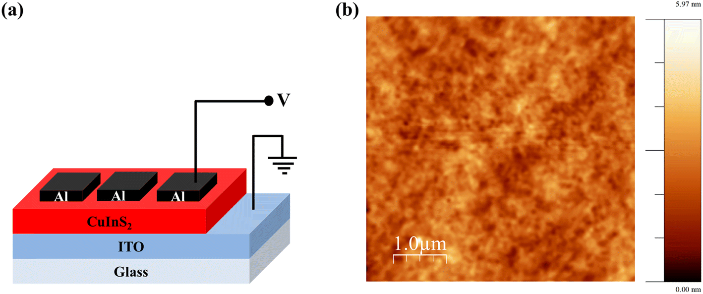 | ||
| Fig. 3 (a) Schematic diagram of Al/CuInS2/ITO device and (b) 5 µm × 5 µm AFM micrograph of CuInS2 film on ITO coated glass substrate. | ||
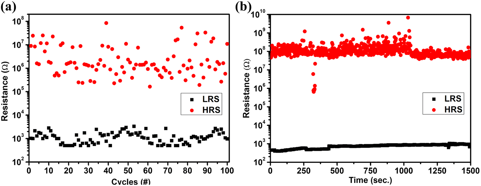
To determine the repeatability of the unipolar RS behavior, 100 SET/RESET switching cycles have been studied on the same device, as shown in Fig. 4(a). The variation in the switching voltage for these 100 cycles is shown in Fig. 4(b). The SET voltage lies in the range of 1.1–2.3 V with a mean of 1.66 V and a standard deviation of 0.3 V. The RESET voltage lies in the range of 0.4–1 V with a mean of 0.69 V and a standard deviation of 0.2 V. Fig. 4(c) and (d) show the histogram plot and the cumulative probability of the SET and RESET voltages with a bin size of 0.05 V. The variation in the resistance of the LRS and HRS for 100 switching cycles is shown in Fig. 5(a). This shows the repeatable performance of the device with a high on/off resistance ratio. The study of HRS and LRS retention at a 0.1 V read voltage revealed the device's ability to sustain state retention for up to 1.5 × 10³ seconds, demonstrating a high on/off ratio of approximately 105, as depicted in Fig. 5(b).
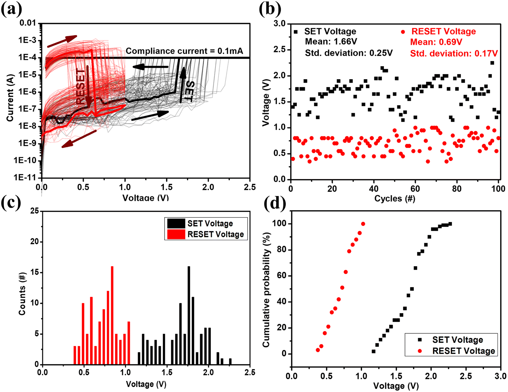 | ||
| Fig. 4 (a) I–V characteristics of Al/CuInS2/ITO memristor device showing unipolar switching for 100 SET/RESET cycles. (b) SET/RESET voltages of 100 cycles. (c) Histogram of SET and RESET voltages with 0.05 V bin size. (d) Cumulative probability of SET/RESET voltages. | ||
 | ||
| Fig. 5 (a) Endurance and (b) retention of the Al/CuInS2/ITO memristor device. | ||
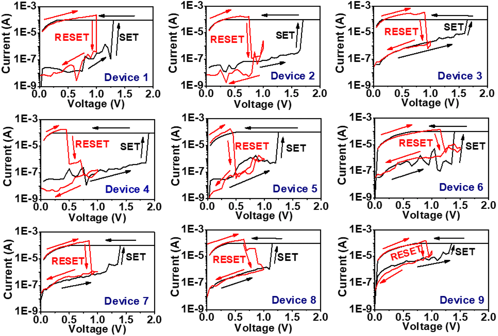
The variation in the device-to-device RS behaviour has also been studied. For this, three different samples of devices have been fabricated keeping all the deposition parameters the same. Three different devices of each sample have been studied for RS behavior.
Fig. 6 shows the RS behaviour of these different 9 devices where devices 1, 2, 3 belong to sample 1; devices 4, 5, 6 belong to sample 2 and devices 7, 8, 9 belong to sample 3. The SET/RESET voltage variation in the devices is shown in Fig. 7(a). This shows the mean of the SET voltages of the devices to be 1.45 V with a standard deviation of 0.2 V and the mean of the respective RESET voltages to be 0.85 V with a standard deviation of 0.2 V. The LRS and HRS resistance of these 9 devices is shown in Fig. 7(b). The resistance of the LRS and HRS states of the devices repeats in the same order with some variations. This shows the device-to-device consistency in unipolar RS behavior for the Al/CuInS2/ITO structure.
 | ||
| Fig. 6 I–V characteristics of 9 different devices. | ||
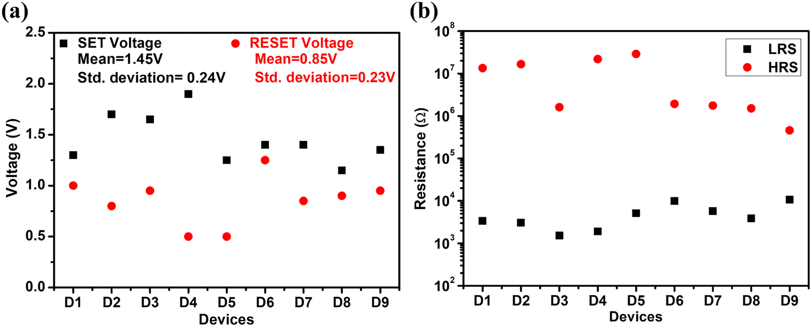 | ||
| Fig. 7 (a) SET/RESET voltage and (b) LRS/HRS resistances of 9 different devices. | ||
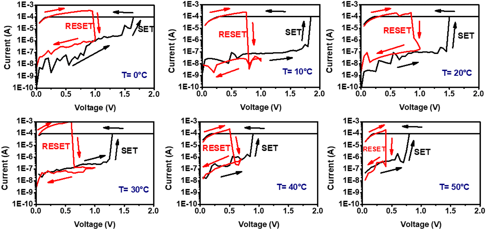
Further, the RS behavior of the device has also been studied at different temperatures in the range of 0 °C to 50 °C. The SET/RESET cycles of the device at the temperatures 0 °C, 10 °C, 20 °C, 30 °C, 40 °C and 50 °C are shown in Fig. 8.
 | ||
| Fig. 8 I–V characteristics of Al/CuInS2/ITO memristor at different temperatures. | ||
The corresponding SET/RESET voltages have been plotted in Fig. 9(a). This shows that the voltage required for both SET and RESET decreases with an increase in temperature. This might be because the thermal energy lowers the required activation energy for the ion.35 Fig. 9(b) shows the device's corresponding LRS and HRS resistance at different temperatures. The HRS resistance is seen to be decreasing with an increase in temperature as CuInS2 QDs exhibit semiconducting behaviour.36
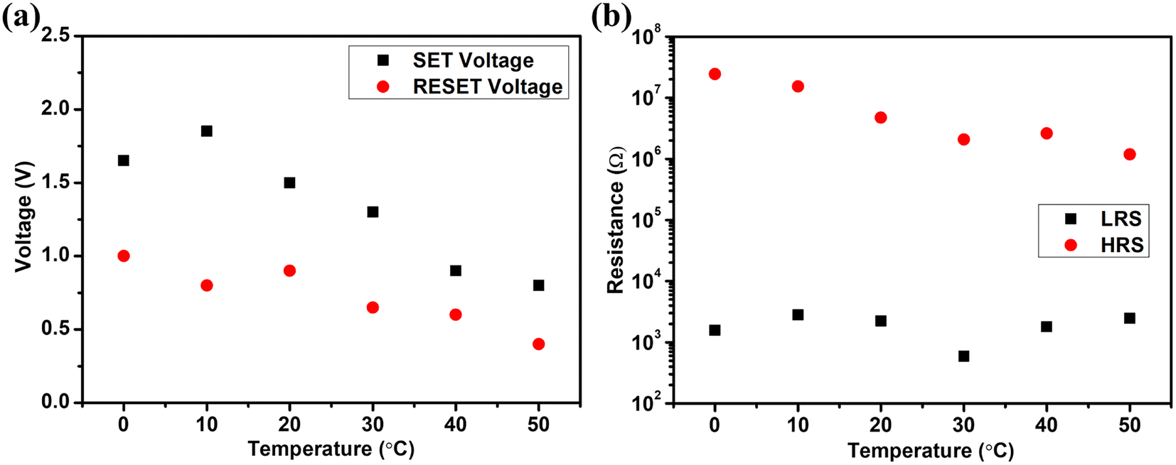 | ||
| Fig. 9 (a) SET/RESET voltages and (b) LRS/HRS resistance of the device at different temperatures. | ||
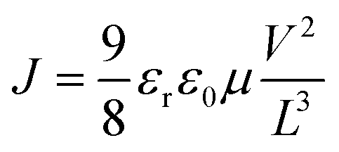
For analyzing the conduction mechanism in the device, the logarithmic V vs. I curves have been plotted for both the SET and RESET processes as shown in Fig. 10(a) and (b) respectively. In the SET process, the device is in the HRS initially, and the current increases linearly with the voltage i.e. ohmic region. As the voltage rises, the current adheres to Child's square law, specifically, I ∝ V2. In this region, the space charge carriers get injected into the trap energy level and the current starts following the Mott–Gurney equation for space charge limited conduction (SCLC).37 This equation is as follows:38
 | (1) |
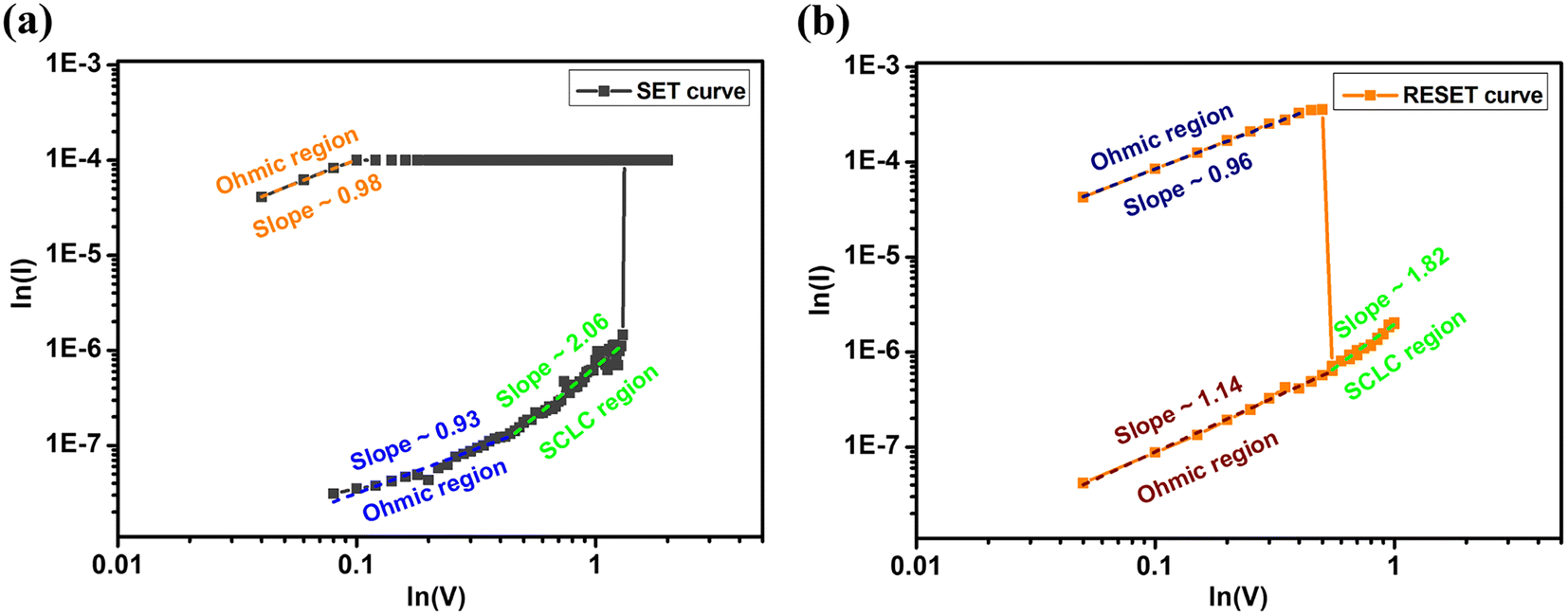 | ||
| Fig. 10 ln(I) vs. ln(V) curves of (a) SET and (b) RESET process. | ||
To further understand the switching mechanism, impedance spectroscopy was performed under a DC voltage of 0.2 V across a frequency range of 500 Hz–1 MHz in both the LRS and HRS of the device. The impedance vs. frequency characteristics for the HRS and LRS are shown in Fig. S2 (ESI†). The Cole–Cole curves i.e. real part of impedance (Z′) vs. imaginary part (Z″) are plotted for both the HRS and LRS states as shown in Fig. 11(a) and (b) respectively. In the HRS state, the Cole–Cole curve shows a semicircular behavior with both imaginary and real parts on the order of 106 Ω. This behavior corresponds to a parallel combination of resistor and capacitor.39 The characteristics of the parallel resistor and capacitor as shown in Fig. 11(a) were fitted to the experimental curve by utilizing the z-simpwin software which gives a series resistance RS = 68.4 Ω, parallel resistance RH = 1.7 MΩ, and parallel capacitance C = 17.5 pF. Thus, the device shows combined capacitive and resistive elemental behavior in the HRS. In the Cole–Cole curve of the LRS, a small horizontal linear behavior is seen as depicted in Fig. 11(b). In this state, the real part lies in the 102 Ω range whereas the imaginary part is negligible in comparison to the real part as seen in Fig. 11(b) (inset). This type of behavior can correspond to a simple resistive component between the electrodes. The increment in the real component with frequency can be attributed to fluctuations in the resistive element, arising from diffusive dynamics within the filamentary component in the LRS. Meanwhile, the diminished imaginary component is ascribed to influences at the interfaces. This study suggests that a resistive filament has formed between the electrodes in the LRS state which was absent in the HRS state. Thus, impedance spectroscopy suggests a filamentary switching mechanism for the RS behavior of the device.
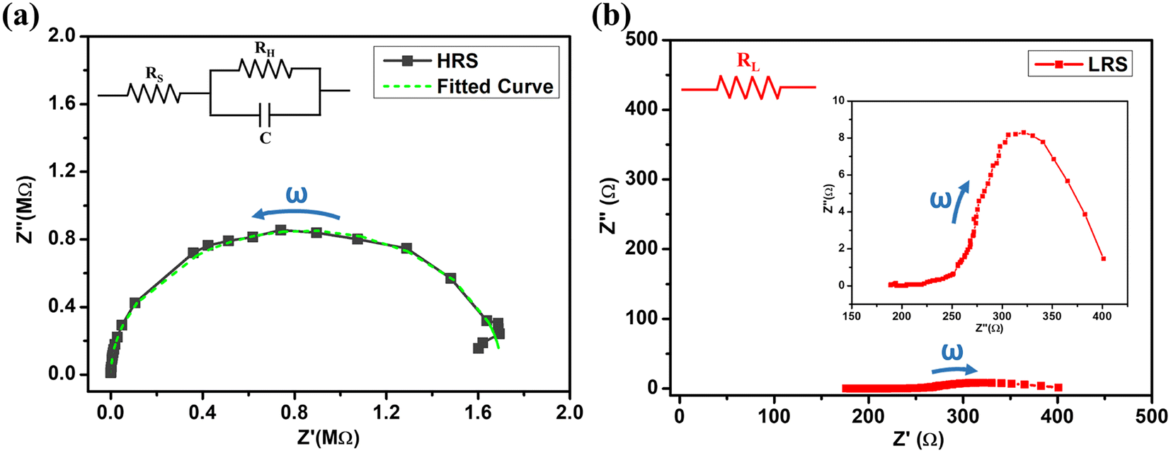 | ||
| Fig. 11 Cole–Cole plots of the device in (a) HRS and (b) LRS. | ||
As impedance spectroscopy reveals a filamentary nature in the LRS, we put forward a filamentary working mechanism to account for the RS behavior of the device, as depicted in Fig. 12. In CuInS2, copper metal ions are present and copper is a highly electrochemically active material. The oxidation of Cu and its migration in the presence of the external electric field give rise to the RS phenomenon in many device structures where Cu is present as an electrode or in the functional layer matrix.15,17,26 The presence of copper ions will have a notable impact on inducing the switching behavior in the device. Initially, the device was in the HRS as shown in Fig. 12(a). As the electric field is applied to the devices, the Cu atoms get oxidized into Cu+ or Cu2+ ions. These ions migrate toward the cathode (ITO electrode) in the presence of an electric field and start accumulating at the CuInS2/ITO interface. These Cu ions get reduced to Cu atoms at the Schottky interface of CuInS2 with ITO. Further increment in the electric field migrates more Cu ions which accumulate to form the conducting filament (CF) between the electrodes. The CF connects both electrodes as shown in Fig. 12(b) and the device gets switched from the HRS to LRS. While forming the filament the compliance current limits the electric field which limits the filament size and the permanent breakdown of the device.
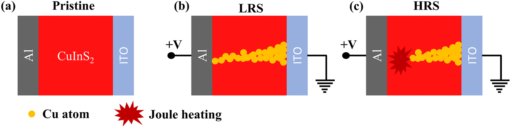 | ||
| Fig. 12 Schematic of filament formation and rupture in the device. | ||
To switch the device back to the HRS, the compliance current limit was removed. This lets the higher current flow through the filament during the RESET process. The higher current creates joule heating in the filament. Due to the joule heating the CF gets ruptured40,41 as shown in Fig. 12(c). This switches the device to the HRS. So, the formation and rupture of the Cu atoms based CF can be the most plausible switching mechanism for the Al/CuInS2/ITO structured RS device. Further, the shorter retention time of the LRS, lasting only up to 1.5 × 10³ s, may be attributed to the diffusive tendencies of the metal cations.42
4 Conclusion
In summary, CuInS2 QDs with a particle size of 2.0 nm have been synthesized via the hot injection method. These QDs are used to fabricate an Al/CuInS2/ITO memristive device that exhibits unipolar RS behavior. The device exhibits consistent switching behaviour for 100 SET/RESET switching cycles. The mean voltages for setting and resetting the device are 1.66 V and 0.69 V respectively. The device retains the LRS and HRS for up to 1.5 × 10³ seconds with a high HRS to LRS resistance ratio of ∼105. For the spatial variance, 9 different devices were tested for the RS behavior and these exhibit the same unipolar RS behavior with minimal variation. The achieved high reproducibility using solution-processable methods represents a significant advancement for mass-producible non-volatile memory applications. The RS behavior at different temperatures has also been studied and the device shows consistency of the unipolar RS behavior in the optimum temperature range of 0–50 °C. For the switching, impedance spectroscopy suggested a filamentary switching mechanism for the RS behaviour. Thus, the formation of the CF due to the migration of Cu+ or Cu2+ ions under the external applied field and rupture of filament due to the joule heating under higher current flow through it has been proposed as a mechanism for the RS behavior in the device. This can be marked as an advancement to establish the switching mechanism in the CuInS2 QDs-based device. These characteristics make CuInS2 QDs suitable for RS-based mass-producible non-volatile memory applications.Author contributions
HS and L synthesized the QDs. HS fabricated the device, analysed the data and prepared the manuscript. HS, NS and DK did the measurements. AK and RS did the overall planning, editing, and supervision of the work.Conflicts of interest
On behalf of all authors, the corresponding authors state that there is no conflict of interest.Acknowledgements
One of the authors, Harshit Sharma, acknowledges UGC for the grant of SRF. The authors are thankful to Dr Rahul Singhal, Department of Physics, MNIT Jaipur, Rajasthan for his help during HRTEM measurements and also to Dr Sushil Kumar, Advanced Materials and Device Metrology Division, CSIR-National Physical Laboratory, New Delhi for his help in impedance spectroscopy measurements.References
- H.-S. P. Wong, H.-Y. Lee, S. Yu, Y.-S. Chen, Y. Wu, P.-S. Chen, B. Lee, F. T. Chen and M.-J. Tsai, Proc. IEEE, 2012, 100, 1951–1970 CAS
.
- R. Waser and M. Aono, Nat. Mater., 2007, 6, 833–840 CrossRef CAS PubMed
- C. Yoshida, K. Tsunoda, H. Noshiro and Y. Sugiyama, Appl. Phys. Lett., 2007, 91, 223510 CrossRef
- B. Hwang and J.-S. Lee, Nanoscale, 2018, 10, 8578–8584 RSC
- N. Saini, A. Bisht, A. Patra and A. Kumar, J. Mater. Sci.: Mater. Electron., 2022, 33, 27053–27061 CrossRef CAS
- D. S. Jeong, R. Thomas, R. Katiyar, J. Scott, H. Kohlstedt, A. Petraru and C. S. Hwang, Rep. Prog. Phys., 2012, 75, 076502 CrossRef PubMed
- D. Ielmini and H.-S. P. Wong, Nat. Electron., 2018, 1, 333–343 CrossRef
- A. Sawa, Mater. Today, 2008, 11, 28–36 CrossRef CAS
- A. R. Patil, T. D. Dongale, R. K. Kamat and K. Y. Rajpure, Mater. Today Commun., 2023, 34, 105356 CrossRef CAS
- F. Zhuge, K. Li, B. Fu, H. Zhang, J. Li, H. Chen, L. Liang, J. Gao, H. Cao and Z. Liu,
et al.
, AIP Adv., 2015, 5, 057125 CrossRef
- J. Jang, F. Pan, K. Braam and V. Subramanian, Adv. Mater., 2012, 24, 3573–3576 CrossRef CAS PubMed
- J. J. Wagenaar, M. Morales-Masis and J. M. Van Ruitenbeek, J. Appl. Phys., 2012, 111, 014302 CrossRef
- F. Zhang, H. Zhang, S. Krylyuk, C. A. Milligan, Y. Zhu, D. Y. Zemlyanov, L. A. Bendersky, B. P. Burton, A. V. Davydov and J. Appenzeller, Nat. Mater., 2019, 18, 55–61 CrossRef CAS PubMed
- L. Yin, R. Cheng, Y. Wen, B. Zhai, J. Jiang, H. Wang, C. Liu and J. He, Adv. Mater., 2022, 34, 2108313 CrossRef CAS PubMed
- R. Guo, L. Zhang, J. Meng, A. Liu, J. Yuan, K. Zheng and J. Tian, Adv. Electron. Mater., 2020, 6, 2000035 CrossRef CAS
- R. Waser, R. Dittmann, G. Staikov and K. Szot, Adv. Mater., 2009, 21, 2632–2663 CrossRef CAS PubMed
- A. Aiba, R. Koizumi, T. Tsuruoka, K. Terabe, K. Tsukagoshi, S. Kaneko, S. Fujii, T. Nishino and M. Kiguchi, ACS Appl. Mater. Interfaces, 2019, 11, 27178–27182 CrossRef CAS PubMed
- H. Sharma, N. Saini, A. Kumar and R. Srivastava, J. Mater. Chem. C, 2023, 11, 11392–11398 RSC
- T. Gao, Q. Zhang, L. Li, X. Zhou, L. Li, H. Li and T. Zhai, Adv. Opt. Mater., 2018, 6, 1800058 CrossRef
- C.-W. Chen, D.-Y. Wu, Y.-C. Chan, C. C. Lin, P.-H. Chung, M. Hsiao and R.-S. Liu, J. Phys. Chem. C, 2015, 119, 2852–2860 CrossRef CAS
- Z. Long, W. Zhang, J. Tian, G. Chen, Y. Liu and R. Liu, Inorg. Chem. Front., 2021, 8, 880–897 RSC
- H. Kim, J. Y. Han, D. S. Kang, S. W. Kim, D. S. Jang, M. Suh, A. Kirakosyan and D. Y. Jeon, J. Cryst. Growth, 2011, 326, 90–93 CrossRef CAS
- M. Lv, J. Zhu, Y. Huang, Y. Li, Z. Shao, Y. Xu and S. Dai, ACS Appl. Mater. Interfaces, 2015, 7, 17482–17488 CrossRef CAS PubMed
- J.-Y. Chang, J.-M. Lin, L.-F. Su and C.-F. Chang, ACS Appl. Mater. Interfaces, 2013, 5, 8740–8752 CrossRef CAS PubMed
- S. Chang, Y. Zhao, J. Tang, Z. Bai, L. Zhao and H. Zhong, J. Phys. Chem. C, 2020, 124, 6554–6561 CrossRef CAS
- Z. Hu, F. Cao, T. Yan, L. Su and X. Fang, J. Mater. Chem. C, 2023, 11, 244–251 RSC
- D. Y. Yun, H. M. Park, S. W. Kim, S. W. Kim and T. W. Kim, Carbon, 2014, 75, 244–248 CrossRef CAS
- T. Ahmad, W. Devulder, K. Opsomer, M. Minjauw, U. Celano, T. Hantschel, W. Vandervorst, L. Goux, G. S. Kar and C. Detavernier, ACS Appl. Mater. Interfaces, 2018, 10, 14835–14842 CrossRef CAS PubMed
- M.-C. Zhu, Y.-J. Shao, J. Zhou, W. Chen, Z.-Q. Wang and J. Tian, Acta Phys. Sin., 2022, 71, 207301 CrossRef
- K. Qi, Y. Wang, R. Wang, D. Wu and G.-D. Li, J. Mater. Chem. C, 2016, 4, 1895–1899 RSC
- R. Xie, M. Rutherford and X. Peng, J. Am. Chem. Soc., 2009, 131, 5691–5697 CrossRef CAS PubMed
- R. Ahmad, U. Soni, R. Srivastava, V. N. Singh, S. Chand and S. Sapra, J. Phys. Chem. C, 2014, 118, 11409–11416 CrossRef CAS
- B. Chen, H. Zhong, W. Zhang, Z. Tan, Y. Li, C. Yu, T. Zhai, Y. Bando, S. Yang and B. Zou, Adv. Funct. Mater., 2012, 22, 2081–2088 CrossRef CAS
- R. Ahmad, R. Srivastava, S. Yadav, D. Singh, G. Gupta, S. Chand and S. Sapra, J. Phys. Chem. Lett., 2017, 8, 1729–1738 CrossRef CAS PubMed
- L. Yin, R. Cheng, Y. Wen, B. Zhai, J. Jiang, H. Wang, C. Liu and J. He, Adv. Mater., 2022, 34, 2108313 CrossRef CAS PubMed
- S. Luo, J. Ke, M. Yuan, Q. Zhang, P. Xie, L. Deng and S. Wang, Appl. Catal., B, 2018, 221, 215–222 CrossRef CAS
- Q. Liu, W. Guan, S. Long, R. Jia, M. Liu and J. Chen, Appl. Phys. Lett., 2008, 92, 012117 CrossRef
-
M. A. Lampert and P. Mark, Current Injection in Solids, Academic Press, 1970 Search PubMed
-
A. Jonscher, Dielectric Relaxation in Solids, Chelsea Dielectrics Press, 1983 Search PubMed
- Y. Wang, H. Liu, X. Wang and L. Zhao, Nanoscale Res. Lett., 2019, 14, 1–9 CrossRef PubMed
- F. Zahoor, T. Z. Azni Zulkifli and F. A. Khanday, Nanoscale Res. Lett., 2020, 15, 1–26 CrossRef PubMed
- Z. Wang, S. Joshi, S. E. Savel'ev, H. Jiang, R. Midya, P. Lin, M. Hu, N. Ge, J. P. Strachan and Z. Li,
et al.
, Nat. Mater., 2017, 16, 101–108 CrossRef CAS PubMed
Footnote |
| † Electronic supplementary information (ESI) available. See DOI: https://doi.org/10.1039/d4ra01087f |
| This journal is © The Royal Society of Chemistry 2024 |