
 Open Access Article
 This Open Access Article is licensed under a Creative Commons Attribution-Non Commercial 3.0 Unported Licence
A first-principles prediction of the structural, electronic, transport and photocatalytic properties of GaGeX3 (X = S, Se, Te) monolayers
Pham D. Trung *a and
Hien D. Tong*b
*a and
Hien D. Tong*b
aYersin University, 27 Ton That Tung, Ward 8, Dalat City, Lam Dong Province, Vietnam. E-mail: phdtrung2018@gmail.com
bFaculty of Engineering, Vietnamese-German University, Binh Duong, Vietnam. E-mail: hien.td@vgu.edu.vn
First published on 17th May 2024
Abstract
The discovery of new 2D materials with superior properties motivates scientists to make breakthroughs in various applications. In this study, using calculations based on density functional theory (DFT), we have comprehensively investigated the geometrical characteristics and stability of GaGeX3 monolayers (X = S, Se, or Te), determining their electronic and transport properties, and some essential optical and photocatalytic properties. AIMD simulations show that these materials are highly structurally and thermodynamically stable. Notably, the GaGeSe3 monolayer is a semiconductor with a band gap of 1.9 eV and has a high photon absorption coefficient of up to 1.1 × 105 cm−1 in the visible region. The calculated solar-to-hydrogen conversion efficiency of the GaGeSe3 monolayer is 11.33%, which is relatively high compared to some published 2D materials. Furthermore, the electronic conductivity of the GaGeSe3 monolayer is 790.65 cm2 V−1 s−1. Our findings suggest that the GaGeSe3 monolayer is a new promising catalyst for the solar water-splitting reaction to give hydrogen and a potential new 2D material for electrical devices with high electron mobility.
1 Introduction
Graphene, the first 2D material discovered, has shown a great combination of superior electronic, mechanical, and thermal properties compared to bulk materials, including the quantum Hall effect, high Young's modulus, high carrier mobility at room temperature, and high thermal conductivity.1 Following the discovery of graphene, a large-scale search has been underway in materials science to discover new 2D materials. A series of new 2D materials have been discovered, such as silicene,2,3 germanene,4 phosphorene,5,6 hexagonal boron nitride (h-BN),7 and transition-metal chalcogenides.8–10 These 2D materials have a unique structure with a high surface-area-to-volume ratio, leading to superior chemical and physical properties compared to bulk materials.11–13 These characteristics offer the potential to achieve outstanding performances when applied in different fields, such as electronics,14–17 sensors,18–20 and catalysis.21–232D chalcogenides have layered structures comprising elements of the chalcogenide group (S, Se, or Te) combined with transition-metal elements.24,25 These materials are atomically thick with many favorable electronic and mechanical properties, making them essential research subjects in nanoelectronics, optoelectronics, sensors,18,26 and energy conversion.27 2D chalcogenides are synthesized using the atomic layer deposition technique, allowing expansion of their industrial applications.24,28 Recently, chalcogenide two-dimensional materials with two transition-metal elements have attracted substantial attention due to the ability to tailor and enrich their structural and electronic properties, which should be due to the presence of a second transition-metal element in the structure.24,29–36
Using first-principles calculations, Hao et al.29 discovered 40 stable 2D materials of the MGeX3 family (M = metallic elements, X = O, S, Se or Te), including eight ferromagnetic, 21 antiferromagnetic, and 11 ferroelectric semiconductors. The MnGeSe3 and MnGeTe3 monolayers are predicted to be ferromagnetic metals at room temperature. Naseri et al.32 demonstrated that 2D XSnS3 (X = Ga, In) monolayers with the space group 162_P![[3 with combining macron]](https://www.rsc.org/images/entities/char_0033_0304.gif) 1m have high energetic, kinetic, mechanical, and thermal stability. The results of Naseri et al. show that the 2D GaSnS3 and InSnS3 monolayers show moderate band gaps (1.34 eV and 1.68 eV, respectively), good absorption of visible light, and consistent band edge positions, indicating that the 2D GaSnS3 and InSnS3 materials are promising photocatalysts for water splitting reactions. Research by Jalil et al.37 discovered that the CoGeSe3 monolayer is a promising 2D photocatalyst due to its moderate band gap (1.508 eV), suitable band edge position, good visible light absorption, and high carrier mobility. Kishore et al.31 discovered new potential catalysts for the water-splitting reaction, including CdPSe3 and ZnPSe3 monolayers, which have low exciton binding energy (in the range of 100–600 meV), high optical absorption (up to 105 cm−1 in the visible region), high carrier mobility with mild anisotropy and moderate external potentials to promote water splitting reactions. The results of Kishore et al.31 and Jalil et al.37 opened up a new solution to promote energy conversion applications by developing new two-dimensional catalytic materials based on elements with high reserves and low costs, to replace the currently used rare metals, such as ruthenium and iridium. However, the big challenge for this group of materials is the limited understanding of the structural characteristics, stability, and electronic, transport, and optical properties of new materials that have not yet been synthesized appropriately in practice.
1m have high energetic, kinetic, mechanical, and thermal stability. The results of Naseri et al. show that the 2D GaSnS3 and InSnS3 monolayers show moderate band gaps (1.34 eV and 1.68 eV, respectively), good absorption of visible light, and consistent band edge positions, indicating that the 2D GaSnS3 and InSnS3 materials are promising photocatalysts for water splitting reactions. Research by Jalil et al.37 discovered that the CoGeSe3 monolayer is a promising 2D photocatalyst due to its moderate band gap (1.508 eV), suitable band edge position, good visible light absorption, and high carrier mobility. Kishore et al.31 discovered new potential catalysts for the water-splitting reaction, including CdPSe3 and ZnPSe3 monolayers, which have low exciton binding energy (in the range of 100–600 meV), high optical absorption (up to 105 cm−1 in the visible region), high carrier mobility with mild anisotropy and moderate external potentials to promote water splitting reactions. The results of Kishore et al.31 and Jalil et al.37 opened up a new solution to promote energy conversion applications by developing new two-dimensional catalytic materials based on elements with high reserves and low costs, to replace the currently used rare metals, such as ruthenium and iridium. However, the big challenge for this group of materials is the limited understanding of the structural characteristics, stability, and electronic, transport, and optical properties of new materials that have not yet been synthesized appropriately in practice.
In this study, via calculations and simulations based on density functional theory (DFT), we have comprehensively investigated the geometrical characteristics and stability of GaGeX3 (X = S, Se, Te) monolayers, determining their electronic, transport, optical, and photocatalytic properties. Our results provide essential data on the fundamental properties of newly studied two-dimensional materials. In particular, in this study, we discovered the GaGeSe3 monolayer as a new candidate for use as a catalyst in the solar water-to-hydrogen splitting reaction and a potential new material in electronic devices with high electron mobility.
2 Methodology
In this study, we performed DFT calculations using the open-source computer code Quantum Espresso.38 The Perdew–Burke–Ernzerhof generalized gradient approximation (PBE-GGA) function has been used to describe the exchange-correlation potential.39 In the optimization and density of states calculations, the k-point grid in the Brillouin zone was set to 15 × 15 × 1 according to the Monkhorst–Pack scheme. The Heyd–Scuseria–Ernzerhof hybrid functional (HSE06) was used to calibrate the electronic bands of the studied materials.40 The van der Waals interaction was taken into account in the calculations using the DFT-D3 approach.41 Kinetic cutoff energies were set to 500 eV. A vacuum layer of 20 Å parallel to the monolayer surface was used to avoid unwanted interactions between periodic slabs in the simulations. The convergence thresholds for force and energy in the ionic and cell optimization calculations were set to 0.01 eV Å−1 and 10−6 eV, respectively. We apply density functional perturbation theory (DFPT) to calculate the phonon spectrum with the help of the PHONOPY package.42 Phonon spectrum calculations were performed with 4 × 4 × 1 supercells of the GaGeX3 (X = S, Se, Te) monolayers. The thermal stability was investigated through ab initio molecular dynamics (AIMD) simulations43 at room temperature.3 Results and discussion
3.1 Structural properties
The optimized structure of the GaGeX3 (X = S, Se, Te) monolayers is shown in Fig. 1a and b. The unit cell of these structures is rhombic in shape and contains two Ga atoms, two Ge atoms, and six chalcogen (S, Se, or Te) atoms. The main structural parameters of the GaGeX3 monolayers were determined after optimization calculations with the PBE functional, and are shown in Table 1. The calculated lattice parameters of the GaGeX3 monolayers are equal to 6.119, 6.457, and 7 Å, respectively, which increase from the top to the bottom of the chalcogen group in the periodic table for S, Se, and Te. In addition, the Ga–X and Ge–X bond distances (X = S, Se, Te) also increase from the top to the bottom of the chalcogen group in the periodic table for S, Se and Te (dGa–S < dGa–Se < dGa–Te and dGe–S < dGe–Se < dGe–Te) (see Table 1). The above fact is explained by the increase in the covalent radii of the chalcogen elements in the order rS < rSe < rTe (by 1.05, 1.20, and 1.38 Å, respectively44) and the decrease in their electronegativity according to order μS > μSe > μTe (corresponding to 2.58, 2.55 and 2.1, respectively).45 | ||
| Fig. 1 The structural model of the GaGeX3 (X = S, Se, Te) monolayers: (a) top view, (b) side view. | ||
| a | dGa–X | dGe–X | dGe1–Ge2 | h | Ecoh | |
|---|---|---|---|---|---|---|
| GaGeS3 | 6.119 | 2.244 | 2.531 | 2.347 | 3.195 | 4.412 |
| GaGeSe3 | 6.457 | 2.390 | 2.670 | 2.388 | 3.383 | 4.024 |
| GaGeTe3 | 7 | 2.605 | 2.884 | 2.445 | 3.636 | 3.589 |
Next, we investigated the structural stability of GaGeX3 (X = S, Se, Te) monolayers by evaluating their energetic, mechanical, dynamical, and thermal stability. In particular, energetic stability is evaluated through the cohesive energy (Ecoh) per atom, which is the average energy (over the number of atoms) to separate the structure into separate atoms:
 | (1) |
The results of calculating the cohesive energies of the GaGeX3 (X = S, Se, Te) monolayers are 4.412, 4.024, and 3.589 eV per atom, respectively. These values are all positive, which allows the prediction that the GaGeX3 (X = S, Se, Te) monolayer structures are energetically stable. Furthermore, it is known that Ecoh is a quantity that characterizes the strength of the bonds between atoms in a material. The greater the cohesive energy, the stronger the bonding force between atoms in the material, which is the basis for the material's mechanical strength. In comparison with previously synthesized 2D materials, we find that the cohesive energies of the GaGeX3 (X = S, Se, Te) monolayers are smaller than those of the MoS2 monolayer (5.02 eV per atom), h-BN monolayer (7.07 eV per atom),46 and graphene (7.85 eV per atom).47 However, the cohesive energies of the GaGeX3 (X = S, Se, Te) monolayers are significantly higher than those of germanene (3.26 eV per atom)48 and phosphorene (3.47 eV per atom).6 These values demonstrate the relatively high motional stability of the studied 2D materials.
We calculated the phonon dispersions to evaluate the dynamical stability of the GaGeX3 (X = S, Se, Te) monolayers, as shown in Fig. 2a. Negative frequencies are absent in the phonon curves of all three materials studied (Fig. 2a). This fact confirms the dynamical stability of the GaGeX3 (X = S, Se, Te) monolayers.
 | ||
| Fig. 2 (a) The phonon dispersions of the GaGeX3 (X = S, Se, Te) monolayers and the energy fluctuations of the GaGeX3 (X = S, Se, Te) unit cells during AIMD simulations at 300 K. (b) The energy fluctuations of the GaGeX3 (X = S, Se, Te) unit cells during AIMD simulations at 300 K. | ||
The thermal stability of the GaGeX3 (X = S, Se, Te) monolayers was evaluated through AIMD simulations. The variation in the total energy over time for the GaGeX3 (X = S, Se, Te) monolayers at room temperature is shown in Fig. 2b. It can be seen that the fluctuation in the total energy of the GaGeX3 (X = S, Se, Te) unit cells is negligible over the simulation period of 10 ps, indicating the high stability of the structure studied at room temperature.
To evaluate the mechanical stability, we use Born's stability criteria for various crystal systems, as clarified in the study of Mouhat et al.49 Specifically, 2D hexagonal structures have mechanical stability when meeting the following conditions: C11 > 0 and C112 > C122.49 The calculated elastic coefficients, as shown in Table 2, show complete satisfaction of the above conditions, confirming the mechanical stability of the GaGeX3 (X = S, Se, Te) monolayers. In addition, the Poisson’s ratios of the GaGeS3, GaGeSe3, and GaGeTe3 monolayers are equal to 0.33, 0.34, and 0.36, respectively, indicating the structural flexibility of these materials under the influence of transverse deformation. These values are also significantly greater than those for graphene (0.19),50 the MoS2 monolayer (0.26), and the GaSe monolayer (0.25),51 indicating more flexibility than graphene and the MoS2 and GaSe monolayers. Furthermore, with the same uniaxial strain (x or y) applied to the three materials studied, the most significant contraction was found in the structure of the GaGeTe3 monolayer in the direction perpendicular to the applied strain. This fact shows that the GaGeTe3 monolayer is more sensitive to horizontal uniaxial deformations than the other two materials.
| C11 | C12 | C66 | Y2D | ν2D | |
|---|---|---|---|---|---|
| GaGeS3 | 83.692 | 27.287 | 28.202 | 74.795 | 0.326 |
| GaGeSe3 | 70.415 | 24.011 | 23.202 | 62.227 | 0.341 |
| GaGeTe3 | 53.92 | 19.384 | 17.268 | 46.952 | 0.36 |
To examine the mechanical properties of the monolayers, we calculated the Young's moduli and Poisson’s ratios in different directions on their horizontal planes, as shown in Fig. 3a and b. It can be seen that the Young's modulus and Poisson’s ratio do not change at all at different angles on the xy-horizontal plane, indicating isotropy in the xy-plane in terms of their mechanical properties.
 | ||
| Fig. 3 The (a) Young's modulus and (b) Poisson’s ratio in the xy-plane of the GaGeX3 (X = S, Se, Te) monolayers. | ||
3.2 Electronic properties
Examination of the band structures shows that the studied monolayers are all indirect semiconductors. The band gaps, calculated based on PBE, of GaGeS3, GaGeSe3, and GaGeTe3 are 1.61, 1.124, and 0.549 eV, respectively. However, the PBE method often results in band-gap calculations that are significantly smaller than the experimental results.41 Meanwhile, the HSE06 functional40 is known to provide band-gap results that are more similar to those from experiments than those from the PBE method are. Therefore, we have additionally calculated the band structures of the GaGeS3, GaGeSe3, and GaGeTe3 monolayers using the HSE06 functional, as shown in Fig. 4 compared with the PBE functional results. The band gaps of the GaGeS3, GaGeSe3, and GaGeTe3 monolayers from the HSE06 functional are 2.511, 1.908, and 1.109 eV, respectively. The projected bands of these monolayers (Fig. 5) show that the valence band maximum (VBM) of the GaGeS3, GaGeSe3, and GaGeTe3 monolayers is mainly formed by the hybridization of the Ge-4s orbitals and the outermost orbital (p) of the chalcogen atoms (S, Se, and Te). The participation of the Ga-4p orbital is insignificant. Meanwhile, the conduction band minimum (CBM) of these 2D materials is formed by the hybridization of Ga-4s and Ge-4s orbitals, and s and p orbitals of the chalcogen atoms (S, Se, and Te) (Fig. 5). | ||
| Fig. 4 Band structures of the GaGeS3, GaGeSe3, and GaGeTe3 monolayers, calculated using PBE/HSE06 methods (cyan/red curves, respectively). | ||
 | ||
| Fig. 5 Projected bands of the GaGeS3, GaGeSe3, and GaGeTe3 monolayers using the HSE06 hybrid functional. | ||
It can be seen that the PBE and HSE06 approximations both give similar results regarding the CBM and VBM positions of the GaGeS3, GaGeSe3, and GaGeTe3 monolayers. The CBM of all three materials is set at the Γ-point, whereas their VBMs are different. Specifically, the VBM of GaGeS3 is located on the line connecting the Γ–M points, while the VBMs of the other two materials are located on the line connecting K–Γ points in the Brillouin zone.
3.3 Transport properties
The carrier mobility was determined to consider the potential applications in electronic devices. The smaller mass of charged particles allows them to move faster depending on the exact value of the external electric field. High mobility of charge carriers in materials is essential for electronic applications.52 The carrier mobility is calculated with the DP method.53 The carrier mobility of 2D materials is calculated according to the formula:
 | (2) |
![[m with combining macron]](https://www.rsc.org/images/entities/i_char_006d_0304.gif) *, and Ed denote the Boltzmann constant, temperature, carrier effective mass, average effective mass, and deformation potential (DP) constant, respectively. The temperature is set to 300 K. The carrier effective mass m* is calculated via parabolic fitting for the VBM and CBM according to the formula:
*, and Ed denote the Boltzmann constant, temperature, carrier effective mass, average effective mass, and deformation potential (DP) constant, respectively. The temperature is set to 300 K. The carrier effective mass m* is calculated via parabolic fitting for the VBM and CBM according to the formula:
 | (3) |
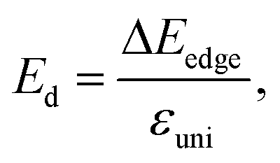
The 2D elastic modulus (C2D) and DP constant (Ed) are calculated according to the formulas:
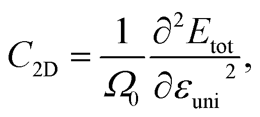 | (4) |
 | (5) |
Here, we have calculated the effective mass (m*), elastic modulus (C2D), deformation potential (Ed), and carrier mobility (μ2D) of the investigated 2D materials along the x- and y-axes, as presented in Table 3. The calculated data in Table 3 show that the carrier mobility of electrons in GaGeS3 and GaGeSe3 is much higher than that of holes. The carrier mobility of the holes of all three 2D structures is approximately equal along the x-and y-axis, indicating the directionally isotropic nature of the electron transport properties. However, for holes, the carrier mobilities of GaGeS3, GaGeSe3, and GaGeTe3 along the x-axis are 1.8, 5.5, and 7.4 times larger than those along the y-axis, indicating high anisotropy of the hole transport. Notably, GaGeSe3 has a high electron mobility of 790.65 cm2 V−1 s−1, much higher than those of monolayer MoS2 (200 cm2 V−1 s−1),54 MoSSe (52.7 cm2 V−1 s−1),55 and WSSe (125 cm2 V−1 s−1).56 These results demonstrate that the GaGeSe3 monolayer is a potential material for application in electronic devices.
| m*x | m*y | C2Dx | C2Dy | Edx | Edy | μ2Dx | μ2Dy | ||
|---|---|---|---|---|---|---|---|---|---|
| Electrons | GaGeS3 | 0.19 | 0.19 | 54.97 | 54.96 | −11.35 | −11.36 | 246.02 | 254.84 |
| GaGeSe3 | 0.12 | 0.12 | 46.49 | 46.49 | −9.70 | −9.71 | 785.15 | 790.65 | |
| GaGeTe3 | 0.55 | 0.49 | 37.06 | 37.04 | −4.42 | −4.42 | 142.27 | 158.39 | |
| Holes | GaGeS3 | 0.96 | 4.70 | 54.97 | 54.96 | −6.66 | −4.10 | 13.01 | 6.96 |
| GaGeSe3 | 0.27 | 1.76 | 46.49 | 46.49 | −6.01 | −5.55 | 146.69 | 26.55 | |
| GaGeTe3 | 0.60 | 4.70 | 37.06 | 37.04 | −6.45 | −6.25 | 18.93 | 2.56 | |
3.4 Photocatalytic properties
For this section, we have investigated some optical properties of the studied monolayer materials, thereby considering their applicability as photocatalysts. It should be noted that the necessary criteria for a photocatalyst in the reaction of splitting water into H2 and O2 include:57–59(1) The band gap needs to be greater than 1.23 eV. This lower limit of the band gap of a photocatalyst is equal to the difference between the potential energy to produce H+ from H2 (−4.44 eV) and the potential energy to produce oxygen from water (−5.67 eV).60 However, a large band gap leads to loss of the ability to convert the energy of photons with energies less than the band gap into energy for stimulating the water-splitting reaction. Related to this issue, Ran et al.61 recommend that the optimal band gap for photocatalysts is about 2.0 eV to balance the requirements between chemical kinetics and light absorption to achieve an effective and high photocatalytic performance for the whole process.
(2) The CBM must be more positive than the water oxidation potential (to produce H2 in the water oxidation reaction), and the VBM must be more negative than the H2O reduction potential (to produce O2 in the dehydration reaction).
(3) A proficient catalytic material should exhibit good absorption capabilities in either the visible or infrared regions, as these two regions collectively represent approximately 43%62 and 51%63 of the solar energy reaching Earth, respectively.
From Fig. 6b, it can be seen that the CBM positions of both the GaGeS3 and GaGeSe3 monolayers are higher than the required reduction potential to produce hydrogen. Meanwhile, their VBM positions are lower than the oxidation potential necessary to generate oxygen. Therefore, it is expected that GaGeS3 and GaGeSe3 monolayers will be able to stimulate the generation of hydrogen and oxygen from water. For the GaGeTe3 monolayer, only its CBM position is suitable to produce hydrogen gas. To clarify the fulfillment of the third criterion above, we calculated the optical absorption coefficients of all three materials according to the formula:
 | (6) |
 | ||
| Fig. 6 (a) The optical absorption spectra of the GaGeS3, GaGeSe3, and GaGeTe3 monolayers at the HSE06 level, compared with solar flux; (b) the band alignments of the studied monolayers in comparison with the oxidation and reduction potentials of water. | ||
Fig. 6a shows the absorption coefficient's dependence on the energy of the solar spectrum. From the optical absorption spectra in Fig. 6a, it can be seen that the GaGeTe3 monolayer strongly adsorbs light in all visible light regions (Ephoton in the range of 1.63–3.26 eV) with an adsorption coefficient in the range of 0.5 × 105 cm−1 to 1.5 × 105 cm−1. The adsorption coefficient of the GaGeTe3 monolayer continues to be maintained at a high level above 1.5 × 105 cm−1 in the ultraviolet region (Ephoton > 3.26 eV). However, the position of the bands of the GaGeTe3 monolayer (Fig. 6b) is not favorable for generating a reduction reaction that produces O2 from H2O, as analyzed above. The GaGeS3 and GaGeSe3 monolayers have lower adsorption coefficients than the GaGeTe3 monolayer in the visible region. The adsorption coefficient of the GaGeSe3 monolayer in the visible light region ranges from 0.1 × 105 cm−1 to 1.1 × 105 cm−1; this coefficient continues to increase strongly in the ultraviolet light region and reaches the maximum value of about 1.4 × 105 cm−1 (at a photon energy of 3.8 eV). This value of the GaGeSe3 monolayer is lower than those of some other potential 2D photocatalysts, such as GeC (2.6 × 105 cm−1),62 arsenene (3.01 × 105 cm−1)63 and MoTe2 (2.90 × 105 cm−1),64 but is more significant than those of GaS (0.71 × 105 cm−1),63 GaSe (0.92 × 105 cm−1)63 and GaN (0.59 × 105 cm−1).65 This characteristic, combined with meeting the first and second criteria mentioned above, suggests that the GaGeSe3 monolayer is a potential photocatalyst in the water-splitting reaction into hydrogen fuel.
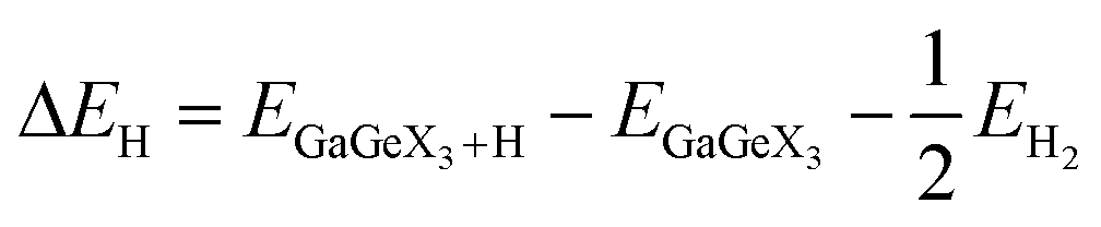
To further clarify the applicability of the GaGeX3 (X = S, Se, Te) monolayers in the water-splitting reaction, we have calculated the Gibbs free energy of hydrogen adsorption (ΔGH) using the formula:66,67
| ΔGH = ΔEH + 0.24 eV, | (7) |
 | (8) |
To facilitate the hydrogen evolution reaction (HER), hydrogen atoms' reversible adsorption and desorption must have small absolute values.68,69 The Gibbs free energies of hydrogen adsorption of the GaGeX3 (X = S, Se or Te) monolayers are calculated to be lowest at site B (the top of the chalcogen atom, see Fig. 7), equal to −2.24 eV, −2.04 eV, and −1.95 eV, respectively These high negative values represent strong interactions between hydrogen atoms and the catalytic surface, limiting the release of H atoms from the catalytic surface, so they predict low water-splitting catalytic performance of these monolayers compared to some other catalysts that have been reported, such as the β-PtSSe monolayer (1.13 eV), WSSe (1.51 eV)70 and Zn2SeTe (1.93 eV).71 However, the Gibbs free energy of hydrogen adsorption on 2D materials can be finely tuned by applying strain, an external electric field, or structural defects,72,73 or changing the pH of the water.74
 | ||
| Fig. 7 (a) Different possible adsorption positions for the HER reaction on the GaGeX3 (X = S, Se, Te) monolayers, (b) the calculated Gibbs free energy of the HER at the B position. | ||
The solar-to-hydrogen (STH) conversion efficiency is known to be an important parameter for evaluating the efficiency of converting solar energy into hydrogen fuel in the water-splitting reaction. This efficiency is determined from the product of the light absorption efficiency and charge-carrier utilization:75
| ηSTH = ηabs × ηcu, | (9) |
The light absorption efficiency is calculated according to the formula:
 | (10) |
 | (11) |
 | (12) |
The band gap of the 2D materials in eqn (12) is calculated at the HSE06 level, which is known to often yield computational values closely matching experimental values.40 The solar-energy conversion efficiencies in the water splitting reaction for the studied 2D materials, calculated using formula eqn (9), are given in Table 4.
| EHSE06g (eV) | χ (H2) | χ (O2) | ηabs (%) | ηCu (%) | ηSTH (%) | |
|---|---|---|---|---|---|---|
| GaGeS3 | 2.51 | 0.59 | 0.69 | 17.46 | 42.36 | 7.39 |
| GaGeSe3 | 1.91 | 0.46 | 0.22 | 37.44 | 30.26 | 11.33 |
| GaGeTe3 | 1.11 | 0.26 | −0.38 | 81.09 | 19.4 | 15.73 |
The calculation results in Table 4 show that the light absorption efficiency (ηabs) and charge-carrier utilization (ηCu) of the studied 2D materials have a close relationship with their band gap. Comparatively, an increase in band gap is accompanied by a decrease in light absorption efficiency and an increase in charge-carrier utilization (Table 4). The GaGeS3 monolayer, featuring the most significant band gap among the studied monolayers (2.51 eV), exhibits the lowest light absorption efficiency of 17.45%. In contrast, the GaGeTe3 monolayer, with the smallest band gap (1.11 eV), possesses the most significant light absorption efficiency of 81.09% and the most minor charge-carrier utilization of 19.4%. Overall, the calculated STH efficiencies of the GaGeS3, GaGeSe3, and GaGeTe3 monolayers are 7.39%, 11.33%, and 15.73%, respectively. The calculated STH efficiency of the GaGeTe3 monolayer is the largest among the studied monolayers. However, the band gap of the GaGeTe3 monolayer is 1.11 eV, which is smaller than the low band gap of traditional photocatalysts.60 Therefore, the GaGeTe3 monolayer is not suitable for application as a photocatalyst in the water-splitting reaction. The STH efficiency of the GaGeSe3 monolayer, equal to 11.33%, is comparable to those of some previously reported 2D photocatalysts, such as the AgBiP2Se6 monolayer (10%),76 Ge2Se2P4 monolayer (12.33%),73 heptazine-based frameworks (12%),77 and Janus WSSe monolayer (11.7%).56 These results show that the monolayer GaGeSe3 is a promising candidate as an photocatalyst in the water-splitting reaction.
4 Conclusion
In this study, we have systematically investigated the structural, electrical, transport, and notable optical and photocatalytic properties of GaGeX3 (X = S, Se, Te) monolayers using DFT calculations. The AIMD simulations highlight the structural and thermodynamic stability of these 2D materials. Notably, the GaGeSe3 monolayer is revealed to be a semiconductor with a band gap of 1.91 eV. In addition, it exhibits a significant photon absorption coefficient in the visible region, with a maximum value of 1.1 × 105 cm−1. The calculated solar-to-hydrogen conversion efficiency of the GaGeSe3 monolayer is 11.33%. The GaGeSe3 monolayer's electronic conductivity has been calculated to be 790.65 cm2 V−1 s−1. These findings suggest that the monolayer GaGeSe3 could be a promising catalyst for solar water-splitting reactions and could advance the field of electronic devices with high electron mobility.Conflicts of interest
There are no conflicts of interest to declare.References
- C. Soldano, A. Mahmood and E. Dujardin, Carbon, 2010, 48, 2127–2150 CrossRef CAS.
- B. Feng, Z. Ding, S. Meng, Y. Yao, X. He, P. Cheng, L. Chen and K. Wu, Nano Lett., 2012, 12, 3507–3511 CrossRef CAS PubMed.
- R. Quhe, R. Fei, Q. Liu, J. Zheng, H. Li, C. Xu, Z. Ni, Y. Wang, D. Yu and Z. Gao, Sci. Rep., 2012, 2, 853 CrossRef PubMed.
- X. Li, S. Wu, S. Zhou and Z. Zhu, Nanoscale Res. Lett., 2014, 9, 1 CrossRef PubMed.
- L. C. Gomes and A. Carvalho, Phys. Rev. B: Condens. Matter Mater. Phys., 2015, 92, 085406 CrossRef.
- J. Guan, Z. Zhu and D. Tománek, Phys. Rev. Lett., 2014, 113, 046804 CrossRef CAS PubMed.
- K. Zhang, Y. Feng, F. Wang, Z. Yang and J. Wang, J. Mater. Chem. C, 2017, 5, 11992–12022 RSC.
- R. Fei, W. Li, J. Li and L. Yang, Appl. Phys. Lett., 2015, 107, 173104 CrossRef.
- L. C. Gomes, A. Carvalho and A. C. Neto, Phys. Rev. B: Condens. Matter Mater. Phys., 2015, 92, 214103 CrossRef.
- H. Wang, H. Yuan, S. Sae Hong, Y. Li and Y. Cui, Chem. Soc. Rev., 2015, 44, 2664–2680 RSC.
- P. Ares and K. S. Novoselov, Nano Mater. Sci., 2022, 4, 3–9 CrossRef CAS.
- L. Daukiya, M. N. Nair, M. Cranney, F. Vonau, S. Hajjar-Garreau, D. Aubel and L. Simon, Prog. Surf. Sci., 2019, 94, 1–20 CrossRef CAS.
- Y. Liu, S. Zhang, J. He, Z. M. Wang and Z. Liu, Nano-Micro Lett., 2019, 11, 1–24 CrossRef CAS PubMed.
- G. Fiori, F. Bonaccorso, G. Iannaccone, T. Palacios, D. Neumaier, A. Seabaugh, S. K. Banerjee and L. Colombo, Nat. Nanotechnol., 2014, 9, 768 CrossRef CAS PubMed.
- F. Schwierz, J. Pezoldt and R. Granzner, Nanoscale, 2015, 7, 8261–8283 RSC.
- M. Huang, X. Jiang, Y. Zheng, Z. Xu, X.-X. Xue, K. Chen and Y. Feng, Front. Phys., 2022, 17, 53504 CrossRef.
- T. V. Vu, B. D. Hoi, A. Kartamyshev and N. N. Hieu, J. Appl. Phys., 2024, 135, 074301 CrossRef CAS.
- N. Joshi, T. Hayasaka, Y. Liu, H. Liu, O. N. Oliveira and L. Lin, Microchim. Acta, 2018, 185, 213 CrossRef PubMed.
- K. D. Pham, T.-D. Hoang, Q.-T. Nguyen and D.-Q. Hoang, J. Alloys Compd., 2023, 940, 168919 CrossRef CAS.
- K. Rajkumar and R. R. Kumar, in Gas Sensors Based on Two-Dimensional Materials and its Mechanisms, Elsevier, 2019, pp. 205–258 Search PubMed.
- G. Guan, E. Ye, M. You and Z. Li, Small, 2020, 16, 1907087 CrossRef CAS PubMed.
- D. Liu, A. Barbar, T. Najam, M. S. Javed, J. Shen, P. Tsiakaras and X. Cai, Appl. Catal., B, 2021, 297, 120389 CrossRef CAS.
- J. Peng, X. Chen, W.-J. Ong, X. Zhao and N. Li, Chem, 2019, 5, 18–50 CAS.
- Y. Kim, W. J. Woo, D. Kim, S. Lee, S.-m. Chung, J. Park and H. Kim, Adv. Mater., 2021, 33, 2005907 CrossRef CAS PubMed.
- X. Yin, C. S. Tang, Y. Zheng, J. Gao, J. Wu, H. Zhang, M. Chhowalla, W. Chen and A. T. Wee, Chem. Soc. Rev., 2021, 50, 10087–10115 RSC.
- X. Tang, A. Du and L. Kou, Wiley Interdiscip. Rev.: Comput. Mol. Sci., 2018, 8, e1361 Search PubMed.
- A. H. Reshak, Appl. Catal., B, 2018, 221, 17–26 CrossRef CAS.
- H. Cai, Y. Gu, Y.-C. Lin, Y. Yu, D. B. Geohegan and K. Xiao, Appl. Phys. Rev., 2019, 6, 041312 Search PubMed.
- K.-R. Hao, X.-Y. Ma, H.-Y. Lyu, Z.-G. Zhu, Q.-B. Yan and G. Su, Nano Res., 2021, 14, 4732–4739 CrossRef CAS.
- T. V. Vu, H. V. Phuc, L. C. Nhan, A. I. Kartamyshev and N. N. Hieu, J. Phys. D: Appl. Phys., 2023, 56, 135302 CrossRef.
- A. Kishore, H. Seksaria, A. Arora and A. De Sarkar, Phys. Chem. Chem. Phys., 2023, 25, 20337–20349 RSC.
- M. Naseri, D. R. Salahub, T. V. Vu and H. Zakaryae, J. Mater. Chem. C, 2022, 10, 11412–11423 RSC.
- T. V. Vu, H. V. Phuc, C. V. Nguyen, V. T. Vi, A. Kartamyshev and N. N. Hieu, Phys. Chem. Chem. Phys., 2022, 24, 16512–16521 RSC.
- R. Xiong, X. Chen, Y. Zhang, Z. Cui, J. Wen, C. Wen, J. Wang, B. Wu and B. Sa, Langmuir, 2023, 39, 15837–15847 CrossRef CAS PubMed.
- Y. Zhang, Y. Shen, J. Liu, L. Lv, M. Zhou, X. Yang, X. Meng, B. Zhang and Z. Zhou, Phys. Chem. Chem. Phys., 2023, 25, 22889–22899 RSC.
- T. V. Vu, H. V. Phuc, A. I. Kartamyshev and N. N. Hieu, Appl. Phys. Lett., 2023, 122, 061601 CrossRef CAS.
- A. Jalil, S. Z. Ilyas, S. Agathopoulos, A. Qureshi, I. Ahmed and T. Zhao, Appl. Surf. Sci., 2021, 565, 150588 CrossRef CAS.
- P. Giannozzi, S. Baroni, N. Bonini, M. Calandra, R. Car, C. Cavazzoni, D. Ceresoli, G. L. Chiarotti, M. Cococcioni and I. Dabo, J. Condens. Matter Phys., 2009, 21, 395502 CrossRef PubMed.
- J. P. Perdew, K. Burke and M. Ernzerhof, Phys. Rev. Lett., 1997, 78, 1396 CrossRef CAS.
- J. Heyd, G. E. Scuseria and M. Ernzerhof, J. Chem. Phys., 2003, 118, 8207–8215 CrossRef CAS.
- S. Grimme, J. Comput. Chem., 2006, 27, 1787–1799 CrossRef CAS PubMed.
- A. Togo, L. Chaput and I. Tanaka, Phys. Rev. B: Condens. Matter Mater. Phys., 2015, 91, 094306 CrossRef.
- S. Nosé, J. Chem. Phys., 1984, 81, 511–519 CrossRef.
- B. Cordero, V. Gómez, A. E. Platero-Prats, M. Revés, J. Echeverría, E. Cremades, F. Barragán and S. Alvarez, Dalton Trans., 2008, 2832–2838 RSC.
- A. L. Allred, J. Inorg. Nucl. Chem., 1961, 17, 215–221 CrossRef CAS.
- Y. Luo, C. Ren, Y. Xu, J. Yu, S. Wang and M. Sun, Sci. Rep., 2021, 11, 19008 CrossRef CAS PubMed.
- L. Caputo, V.-H. Nguyen and J.-C. Charlier, Phys. Rev. Mater., 2022, 6, 114001 CrossRef CAS.
- L.-M. Yang, I. A. Popov, T. Frauenheim, A. I. Boldyrev, T. Heine, V. Bačić and E. Ganz, Phys. Chem. Chem. Phys., 2015, 17, 26043–26048 RSC.
- F. Mouhat and F.-X. Coudert, Phys. Rev. B: Condens. Matter Mater. Phys., 2014, 90, 224104 CrossRef.
- A. Politano and G. Chiarello, Nano Res., 2015, 8, 1847–1856 CrossRef CAS.
- M. Yagmurcukardes, R. T. Senger, F. M. Peeters and H. Sahin, Phys. Rev. B, 2016, 94, 245407 CrossRef.
- Y. Shirota and H. Kageyama, Chem. Rev., 2007, 107, 953–1010 CrossRef CAS PubMed.
- J. Bardeen and W. Shockley, Phys. Rev., 1950, 80, 72 CrossRef CAS.
- B. Radisavljevic, A. Radenovic, J. Brivio, V. Giacometti and A. Kis, Nat. Nanotechnol., 2011, 6, 147 CrossRef CAS PubMed.
- L. Ju, M. Bie, J. Shang, X. Tang and L. Kou, J. Phys Mater., 2020, 3, 022004 CrossRef CAS.
- L. Ju, M. Bie, X. Tang, J. Shang and L. Kou, ACS Appl. Mater. Interfaces, 2020, 12, 29335–29343 CAS.
- S. Nishioka, F. E. Osterloh, X. Wang, T. E. Mallouk and K. Maeda, Nat. Rev. Methods Primers, 2023, 3, 42 CrossRef CAS.
- G. Wang, J. Chang, W. Tang, W. Xie and Y. S. Ang, J. Phys. D: Appl. Phys., 2022, 55, 293002 CrossRef CAS.
- D. Yao, L. Gu, B. Zuo, S. Weng, S. Deng and W. Hao, Nanoscale, 2021, 13, 10624–10648 RSC.
- J. Schneider, M. Matsuoka, M. Takeuchi, J. Zhang, Y. Horiuchi, M. Anpo and D. W. Bahnemann, Chem. Rev., 2014, 114, 9919–9986 CrossRef CAS PubMed.
- J. Ran, J. Zhang, J. Yu, M. Jaroniec and S. Z. Qiao, Chem. Soc. Rev., 2014, 43, 7787–7812 RSC.
- K. Ren, C. Ren, Y. Luo, Y. Xu, J. Yu, W. Tang and M. Sun, Phys. Chem. Chem. Phys., 2019, 21, 9949–9956 RSC.
- J. Li, Z. Huang, W. Ke, J. Yu, K. Ren and Z. Dong, J. Alloys Compd., 2021, 866, 158774 CrossRef CAS.
- C. Shao, K. Ren, Z. Huang, J. Yang and Z. Cui, Front. Chem., 2022, 10, 847319 CrossRef CAS PubMed.
- K. Ren, Y. Luo, J. Yu and W. Tang, Chem. Phys., 2020, 528, 110539 CrossRef CAS.
- J. K. Nørskov, T. Bligaard, A. Logadottir, J. Kitchin, J. G. Chen, S. Pandelov and U. Stimming, J. Electrochem. Soc., 2005, 152, J23 CrossRef.
- F.-S. Zhang, J.-W. Wang, J. Luo, R.-R. Liu, Z.-M. Zhang, C.-T. He and T.-B. Lu, Chem. Sci., 2018, 9, 1375–1384 RSC.
- C. Tsai, K. Chan, J. K. Nørskov and F. Abild-Pedersen, Catal. Sci. Technol., 2015, 5, 246–253 RSC.
- Q. Wang, Z. L. Zhao, S. Dong, D. He, M. J. Lawrence, S. Han, C. Cai, S. Xiang, P. Rodriguez and B. Xiang, Nano Energy, 2018, 53, 458–467 CrossRef CAS.
- P. Jamdagni, A. Kumar, S. Srivastava, R. Pandey and K. Tankeshwar, Phys. Chem. Chem. Phys., 2022, 24, 22289–22297 RSC.
- X. Tan, Q. Chen, Y. Liang, Z. Tian, T. Gao and Q. Xie, Int. J. Hydrogen Energy, 2024, 51, 222–230 CrossRef CAS.
- Z. Haman, N. Khossossi, M. Kibbou, I. Bouziani, D. Singh, I. Essaoudi, A. Ainane and R. Ahuja, Appl. Surf. Sci., 2022, 589, 152997 CrossRef CAS.
- T. V. Vu, N. N. Hieu, D. D. Vo, A. Kartamyshev, H. D. Tong, T. T. Trinh, V. Khuong Dien, Z. Haman, P. Dey and N. Khossossi, J. Phys. Chem. C, 2024, 128, 4245–4257 CrossRef CAS.
- M. Jakhar and A. Kumar, J. Mater. Chem. A, 2022, 10, 6785–6795 RSC.
- C.-F. Fu, J. Sun, Q. Luo, X. Li, W. Hu and J. Yang, Nano Lett., 2018, 18, 6312–6317 CrossRef CAS PubMed.
- L. Ju, J. Shang, X. Tang and L. Kou, J. Am. Chem. Soc., 2020, 142, 1492–1500 CrossRef CAS PubMed.
- Y. Zhao, C. Wang, X. Han, Z. Lang, C. Zhao, L. Yin, H. Sun, L. Yan, H. Ren and H. Tan, Adv. Sci., 2022, 9, 2202417 CrossRef CAS PubMed.
| This journal is © The Royal Society of Chemistry 2024 |