
 Open Access Article
 This Open Access Article is licensed under a Creative Commons Attribution-Non Commercial 3.0 Unported Licence
First-principles study on the electronic properties of biphenylene, net-graphene, graphene+, and T-graphene based nanoribbons†
Wensheng Zhou‡
a,
Cheng Luo‡a,
Yun Chao*a,
Songbo Xionga,
Menegqiu Long c and
Tong Chen*ab
c and
Tong Chen*ab
aEnergy Materials Computing Center, Jiangxi University of Science and Technology, Nanchang 330013, PR China. E-mail: 279916153@qq.com
bState Key Laboratory of Surface Physics and Department of Physics, Fudan University, Shanghai 200433, PR China. E-mail: chentong@jxust.edu.cn
cHunan Key Laboratory of Super Micro-structure and Ultrafast Process, Central South University, Changsha 410083, China
First published on 7th March 2024
Abstract
Since the successful separation of graphene, carbon materials with the excellent physical and chemical properties have attracted the interest of a large number of researchers. In this paper, density functional theory combined with non-equilibrium Green's function is used to systematically study the electronic structures of two-dimensional biphenylene, net-graphene, graphene+ and T-graphene, and to reveal the electron transport properties of net-graphene nanodevices under asymmetric regulation. The results show that biphenylene, net-graphene, graphene+, and T-graphene all show metallic properties, in which biphenylene and net-graphene show anisotropy, while graphene+ and T-graphene show isotropy. In addition, for the one-dimensional new carbon based nanoribbons, except for the armchair-edged net-graphene and biphenylene nanoribbons, which exhibit semiconductor properties and a band gap value of 0.08 eV, the rest of the carbon nanoribbons display metal properties. Interestingly, two of them showed a tendency to oscillate and decrease the band gap value with increasing width, while BPN-2 biphenylene nanoribbons directly changed from exhibiting semiconductor to metallic properties with increasing width combination with no oscillation. The electronic transport properties of net-graphene nanoribbons based nanodevice models for electrons transform along zigzag and armchair directions are systematically studied. An obvious negative differential resistance characteristic along the armchair and zigzag directions can be found. Overall, these interesting results show that these new net-graphene nanodevices have good practical application prospects in future electronic nanodevices.
1. Introduction
In 2004, Novoselov and Geim successfully produced graphene as a material using the micro-mechanical stripping method,1 overturning the previous view in the field of condensed matter physics that 2D materials cannot exist at finite temperatures. At this point, the substantive application of 2D materials truly begun. A large number of research experiments have proven that graphene has strong thermal conductivity,2 stable chemical properties,3 and important application prospects in mechanics,4 electricity,5 optics,6 thermodynamics,7 and other fields.8–10 In addition, the electronic properties of graphene can be adjusted through doping,11 stretching,12–14 and introducing defects.15 Therefore, graphene has great development prospects16 in fields such as sensors,17–19 transistors,20–22 flexible display screens,23–25 and photosensitive components.26–28 Meanwhile, many new carbon materials have been proposed by altering the spatial distribution of carbon atoms within 2D carbon isomers. For example, a four asymmetric carbon isomer referred to as T-graphene has theoretical energy substitutability and kinetic stability and Dirac-like fermions, despite its non-equivalent bonds and non-comb-like structure.29 Fan et al.30 and Liu et al.31 successfully synthesized flat biphenylene and net-graphene composed of four, six, and eight cyclic arrangements, respectively. The 2D carbon isomerization of non-hexagonal rings has become a reality. According to reports, these two materials seem to have electronic properties similar to graphene, and their electronic properties seem even more eye-catching.32,33 Subsequently, Chen et al. found that nitrogen-doped or boron-doped double T-graphene has excellent desorption temperature, ideal adsorption energy, and high hydrogen storage capacity, making it a promising hydrogen storage material.34 Li et al. used density functional theory combined with Grüneisen's theory and found that monolayer biphenylene exhibits anisotropy and negative internal thermal expansion.35 In addition, Tong et al. found that biphenylene, T-graphene, and net-graphene capture three-phonon, four-phonon, and phonon electron interactions, which are dramatically reduced compared to the original graphene, exhibiting ultra-high electronic thermal conductivity.36 In 2022, Yu et al. and Qin et al. reported a new type of carbon single-layer graphene+ mixed through sp2–sp3 hybridization. This new carbon material not only inherits the Dirac properties of pentagonal graphene, but also has better energy stability.37,38With the development of 2D materials, many researchers have become interested in one-dimensional (1D) nanoribbons.39,40 Based on extensive research, graphene nanoribbons (GNR) are a quasi-1D carbon nanomaterial. Due to their two edge structures breaking or affecting the large π bonds in graphene, they alter the ideal uniform electronic structure of graphene. Therefore, GNR has strong edge effects and complex electrical properties.41,42 In addition, GNR can be divided into basic armchair graphene nanoribbons (AGNR) and zigzag graphene nanoribbons (ZGNR) due to their different edges. In the study of AGNR, Saraswat et al. synthesized AGNR from the bottom up on the epitaxial layer of Ge on Si (001) through chemical vapor deposition.43 Cunha et al. found that the polaron properties of AGNR are influenced by their width and size.44 Cloke et al. found that carbon atoms at specific positions in armchair graphene can be replaced with B atoms to change its original band structure and charge carrier concentration.45 Neto et al. found the existence of optoelectronic properties in AGNR based on the dynamics of the photo generation process and the structural characteristics of the system.46 Nguyen et al. found that in the presence of an electric field, the bilayer AGNR exhibits lower threshold absorption frequency, more absorption peaks, and weaker spectral intensity. When the electric field intensity is increased, the prominent peak of edge-related selection rules decreases, and sub-peaks that meet additional selection rules appear.47 In the study of zigzag-edged graphene, Ruffieux et al. synthesized ZGNR from the bottom up through surface-assisted polymerization and cyclization dehydrogenation of specially designed precursor monomers.48 Wang et al. found that the edge state of double-layer ZGNRs can be changed by modulating the twist angle and stacking offset.49 Blackwell et al. discovered spin splitting by introducing alternative N atom dopants at the edges of zigzag graphene.50 Magda et al. found that as the width of ZGNRs increases, there is a transition from metallicity to semiconductor, and the magnetic properties on the edges of ZGNR can remain stable at room temperature.51 Wang et al. reported that the edge state of twisted double-layer ZGNR can be adjusted by twisting angle and stacking offset.52 Further research has explored the properties of GNR along the armchair and zigzag directions more thoroughly.
In recent years, with increasing global attention to environmental and energy issues, the low-carbon economy and clean energy have become hot topics worldwide. As an important component, the research on new carbon based materials has also received increasing attention. Inspired by it, this article conducted a systematic study on four kinds of new carbon based materials. Firstly, we constructed 2D structures of biphenylene, graphene+, net-graphene, and T-graphene and analyzed their electronic properties. It was found that graphene+ and T-graphene exhibit isotropy, while biphenylene and net-graphene exhibit anisotropy. Subsequently, through boundary unsaturation, two opposing edges of the 2D material were passivated with hydrogen atoms to stabilize their charges, and eight 1D new carbon based nanoribbons of these four new carbon based materials were constructed and their electronic properties were explored. Then, nanoribbons with different widths of biphenylene and net-graphene were constructed, and the trend of band gap variation with different widths was analyzed. Finally, we constructed an electronic device with asymmetric regulation of net-graphene, and systematically analyzed their transmission characteristics. This paper could provide some help for the direction of future research into new carbon nanodevices.
2. Calculation methods
All calculation results were calculated using the Atomistix ToolKit (ATK) software package based on density functional theory (DFT) combined with non-equilibrium Green's function (NEGF).53–55 To avoid the interaction between carbon isomers and periodic images, a vacuum layer of at least 15 Å should be retained in the Z direction. All calculated Fermi levels are set to zero. To ensure the convergence properties of the material, the calculation is completed when the atomic force is set to be less than 0.05 eV Å−1. In addition, the k-points grid 1 × 1 × 150 is used to sample the Brillouin zone of electrodes in the x-, y-, and z-directions (transport direction), the calculated temperature is set to 300 K, and the cutoff energy of 370 Ry and atomic force of 0.05 eV Å−1 are used in the calculation process. The current through the device can be calculated using the Landauer−–Büttiker formula:
 | (1) |
3. Results and discussion
3.1 Electronic structure of 2D novel carbon materials
To explore the practical application prospects of 2D materials, one must first start by studying their electronic structure. The optimized structures of four kinds of new carbon based materials, named biphenylene,56 net-graphene, graphene+,38 and T-graphene29 unit-cells, as well as their corresponding phonon spectra, energy bands, and density of states (DOS), are shown from left to right in Fig. 1 and S1.† The blue dotted box represents the cells of each new carbon based materials. The unit-cell structures of biphenylene and net-graphene are rectangular, with lattice arguments of a = 3.75 Å, b = 4.25 Å and a = 6.27 Å, b = 4.39 Å, respectively. The unit-cell structures of graphene+ and T-graphene are standard squares, with lattice arguments of a = b = 6.64 Å and a = b = 3.46 Å, respectively.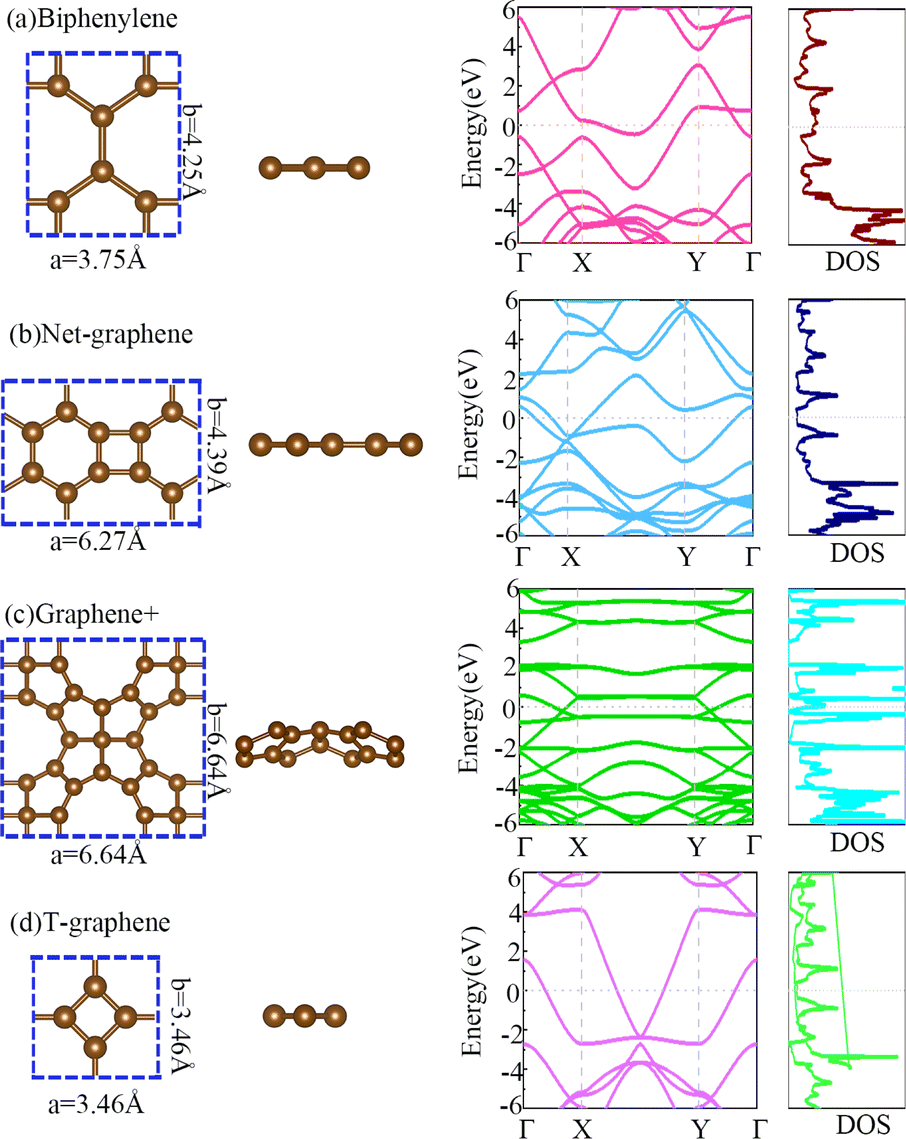 | ||
| Fig. 1 Unit-cell structure, side view, energy band, and density of states (DOS) of (a) biphenylene, (b) net-graphene, (c) graphene+ and (d) T-graphene. The blue dotted box represents the cells of each structure. Set the zero energy level to the Fermi level, represented by a gray horizontal dotted line. | ||
In addition, from the side view of the structure, it can be seen that all carbon atoms of biphenylene, net-graphene, and T-graphene are in the same plane, while all carbon atoms of graphene+ are not in the same plane with an undulating fold structure. Analyzing the phonon spectra of biphenylene, net-graphene, graphene+, and T-graphene, it can be seen that there is no virtual frequency in the phonon spectra, and the structure is dynamically stable. Surprisingly, graphene + exhibits two different Dirac cones on the highly symmetric path of the energy band structure between Γ and X, as well as between Γ and Y, indicating that graphene+ is a Dirac metal material. In addition, due to the high symmetry of the energy band structures of graphene+ and T-graphene between Γ and X and between Γ and Y, indicates that both graphene+ and T-graphene exhibit isotropy. Nevertheless, Fig. 1(c and d) show that the unsymmetry of the energy band structures of net-graphene and biphenylene between Γ and X and between Γ and Y, indicates that both net-graphene and biphenylene exhibit anisotropic properties.
3.2 Electronic structure of one-dimensional new carbon based material nanoribbons
When 2D materials are prepared into 1D nanoribbon structures, due to the confinement effect in the width direction and the difference in edge structure, they have unique electrical, optical, and magnetic properties that are different from 2D materials.57–61 In order to further explore the characteristics of new carbon based materials nanoribbons with different edge styles, we constructed and calculated 1D nanoribbons (a)–(h) and band diagrams (i)–(p) of biphenylene, graphene+, net-graphene, and T-graphene with zigzag and armchair edges with approximate equal width in Fig. 2. To facilitate the distinction between the types and directions of nanoribbons, we use abbreviated names such as BPN-1, BPN-2, G+1, G+2, N-1, N-2, T-1, and T-2 instead of their full names. By analyzing the energy band diagram, the energy band of N-2 does not cross the Fermi level, and forms a band gap with a width of 0.08 eV near the Fermi level.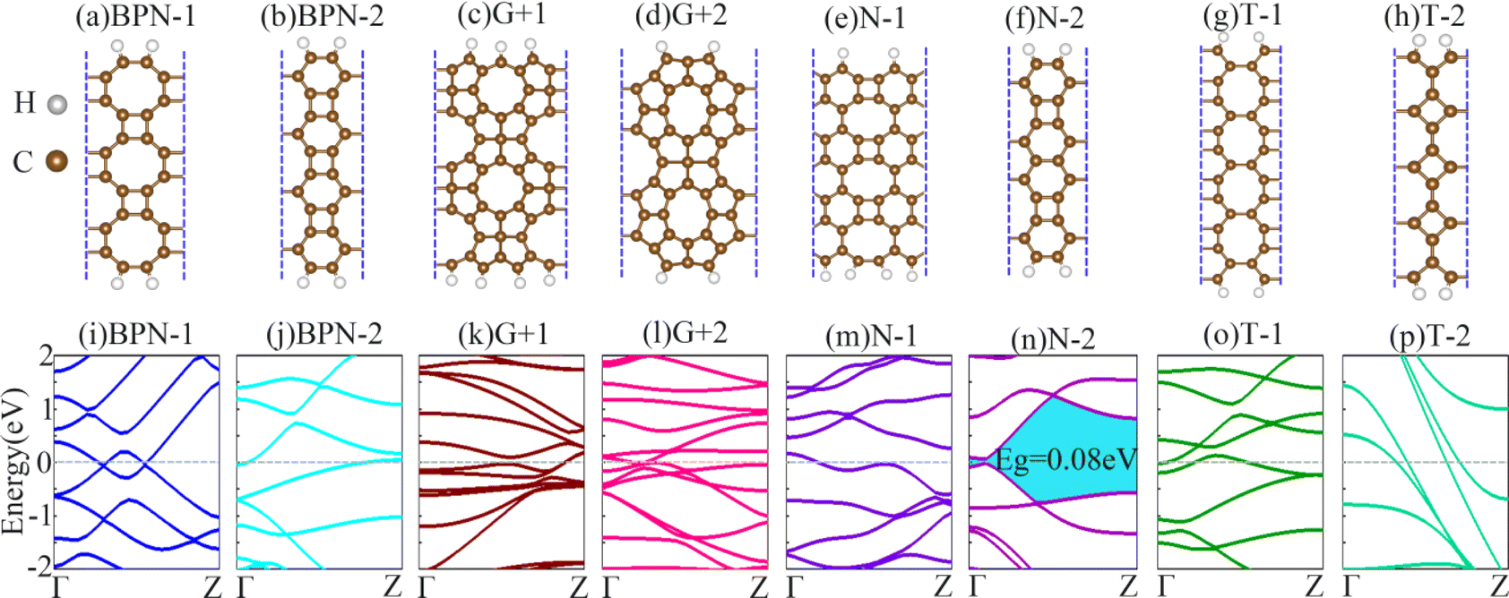 | ||
| Fig. 2 (a)–(h) show two types of nanoribbon structures of biphenylene, graphene+, net-graphene, and T-graphene, respectively, with the energy band diagrams of each type corresponding to (i)–(p). Set the zero energy level to the Fermi level, represented by a gray horizontal dotted line. The gray white sphere represents H, and the golden yellow represents C. | ||
The energy band gap refers to the energy difference between the valence band and the conduction band, which is the minimum energy required for electrons to transition from the valence band to the conduction band region. To some extent, the energy band gap determines the conductivity of a solid material. In general, the smaller the energy band gap, the better the conductivity of the material. This is because the smaller the energy band gap, the smaller the energy difference between the valence band and the conduction band, and the more easily electrons are excited into the conduction band to form a current. For example, the energy band gap of metals is 0 eV, making it easier for electrons to be excited into the conduction band to form current, so metals have good conductivity. On the contrary, insulators have a very large energy band gap, and the energy difference between the valence band and the conduction band is large. It is difficult for electrons to be excited into the conduction band to form a current, so insulators do not conduct electricity. The energy band gap of semiconductors is between metals and insulators, with a moderate gap size and conductivity between metals and insulators. Therefore, N-2 nanoribbons with moderate energy band gaps exhibit semiconductor properties. The energy bands of the other seven metal structures all pass through the Fermi level, with a zero energy band gap. There is a large amount of electron level overlap between the valence band and the conduction band, and electrons are prone to freely jump to the conduction band. Therefore, nanoribbons have good conductivity and exhibit significant metal properties.
Due to the metallic nature of G+1, G+2, N-1, T-1, and T-2 nanoribbons, and the metallicity does not change significantly with the width of the ribbons. While N-2, BPN-1 and BPN-2 nanoribbons are typical semiconductor properties with band gaps varying with width. In order to further analyze the relationship between the electronic properties and width adjustment of nanoribbons in the N-2, BPN-1, and BPN-2 directions. As shown in Fig. 3, we constructed a trend chart of the nanoribbons structures Nx, Bm, and Bn (x values range from 6 to 20, m values range from 6 to 12, and n values range from 6 to 12) for N-2, BPN-1, and BPN-2 at different widths to study the band gap of the nanoribbons changing with width. We can find many interesting results from the trend chart of band gap changes. If the band gap of Nx nanoribbons is zero at x = 15, N15 nanoribbons exhibit metallic properties, while at other widths, nanoribbons exhibit semiconductor properties. More interestingly, the band gap values of x show a shock trend from 6–11 to 15–20. The band gap of Nx nanoribbons shows an overall trend of decreasing oscillation under the adjustment of width. When m is taken as 8, 12, and n is taken as 11, 12, respectively, the band gap of Bm and Bn nanoribbons is zero, exhibiting the metallic properties at the widths. The band gap of Bm nanoribbons shows an overall oscillation decreasing trend under width adjustment, while the band gap of Bn nanoribbons shows a continuous decreasing trend to zero under width adjustment. In summary, the electronic properties of nanoribbons in the N-2, BPN-2, and BPN-2 directions are all affected by width regulation, achieving the conversion between semiconductor and metal properties. By utilizing this property, the electronic properties of such nanoribbons by changing their width can be modulated. This also provides us with a choice in building electronic devices and helps us make more types of electronic devices.
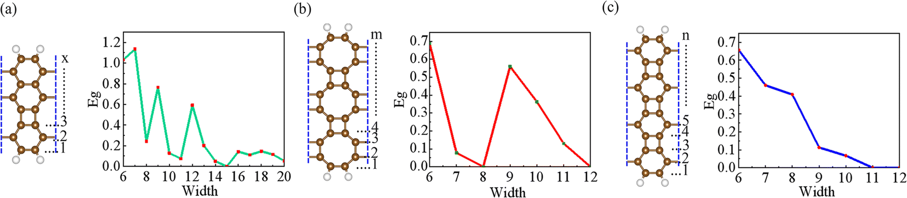 | ||
| Fig. 3 (a) Trend chart of the nanoribbons structure and band gap of net-graphene in the N-2 nanoribbons direction as a function of width. (b) The variation of the nanoribbons structure and band gap of biphenylene with different widths of the BPN-1 nanoribbons. (c) The trend chart of the variation of the nanoribbons structure and band gap of biphenylene in the BPN-2 nanoribbons direction with the width. In the trend chart, the level X-axis represents the width of the band, and the perpendicular Y-axis represents the size of the band gap. | ||
3.3 Transmission characteristics of net-graphene nanodevices
Inspired by this, we constructed two types of nanodevices A11-p and Z8-q along the armchairs and zigzags of net-graphene. A11-p and Z8-q are named based on the characteristics of the two-probe nanodevices. A and Z represent nanodevices along the armchair and zigzag directions of net-graphene, respectively. 11 and 8 represent the fixed width of the left half of the two devices, while p and q represent the variable width values of the right half of these two devices, respectively. Among them, the device consists of a finite intermediate scattering region and two semi-infinite left (L) and right (R) electrodes. There are certain differences in the conductivity of quasi 1D nanoribbons of net-graphene in the armchair and zigzag directions. Additionally, the conversion of nanoribbons between metal and semiconductor properties can be achieved by changing the width of net-graphene nanoribbons. In order to further explore the transport characteristics of A11-p and Z8-q nanodevices at different widths of p and q. Moreover, we calculated the current–voltage (I–V) characteristic curves, transmission spectra, and transport state maps of A11-p and Z8-q devices at different widths of p and q.Fig. 4(c) shows the I–V characteristic curves of A11-p devices at the bias voltage range of −2–2 V, and the I–V characteristic curves of Z8-q devices from −2 V to 2 V. Where p and q represent the width of the right half of the device. Take device A11-p as an example, when the number of layers in the right half of the device is 5, p = 5, and the device is named A11-5; when the number of layers is 6, p = 6, and the device name is A11-6. Of course, the same applies to device Z8-q. We first analyze the I–V characteristic curves of A11-p nanodevices, and it is not difficult to find two eye-catching curves, A11-6 and A11-10, which exhibit diametrically opposite results. The currents of the A11-6 device almost keep zero from −2–2 V, while the currents of the A11-10 device always with the highest values at the respective bias voltage, indicating that the conductivity of the A11-6 device is very poor, while the A11-10 device have good conductivity. Among them, the current of the A11-10 device increases with the increase of bias voltage when the bias voltage is 0–1.6 V, reaching a maximum value of 53.97 μA at 1.6 V, showing the strong metallicity. However, the current decreases with the increase of bias voltage at 1.6–2 V, indicating that the A11-10 device have a good NDR effect. Therefore, the A11-10 device have potential applications in logic gates,62 amplifiers,63 and high-frequency oscillators.64–66 Further analysis of the I–V characteristic curves of the remaining devices reveals the presence of NDR effects in all of them. Next, we analyze the I–V characteristic curves with zigzag-edged based net-graphene nanoribbon of Z8-q nanodevices in Fig. 4(d), and we can find that Z8-q nanodevices do not exhibit the similar eye-catching I–V curves of A11-p devices, and they are basically concentrated in a certain region of variation. The Z8-5 and Z8-7 devices have relatively good conductivity under full bias voltage. Compared to other Z8-q devices with different widths, the current of Z8-5 and Z8-7 devices is relatively high throughout the entire bias voltage range. Among them, the Z8-5 and Z8-7 devices reach maximum currents of 34.76 μA and 42.06 μA at bias voltages of 1.2 V and 1.6 V, respectively, while the Z8-4 devices have relatively low currents throughout the entire bias voltage range and exhibit poor conductivity. Further analysis of the I–V characteristic curve of the Z8-q device reveals that there is also a significant NDR effect in the device.
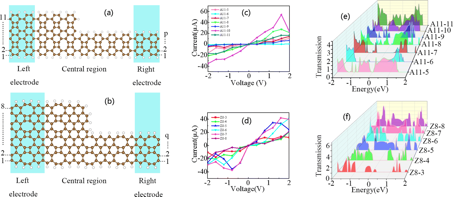 | ||
| Fig. 4 (a and b) Schematic diagram of A11-p and Z8-q nanodevice model based on net-graphene nanoribbons along armchair and zigzag direction. Where p and q represent the width of the right half of the nanodevice, and a light blue box represents the left and right electrodes. (c and d) I–V characteristic curves of A11-p and Z8-q nanodevices. (e and f) Transmission spectra of A11-p and Z8-q nanodevices with different widths under zero bias voltage. The color of the transmission spectrum is consistent with the I–V characteristic curve. The Fermi energy levels are all set to 0 eV. | ||
Similarly, in order to understand the effect of width on the electronic transport properties of A11-p and Z8-q nanodevices under asymmetric regulation, we calculated and plotted the zero bias electron transmission spectra of A11-p and Z8-q model devices, as shown in Fig. 4(e and f). It can be observed that there are many peaks in the transmission spectrum of the A11-p device, indicating that the device has good transport properties. Devices of A11-6, A11-7, and A11-9 exhibit a large transmission gap near the Fermi level, and the transmission peak of the nanodevice is completely suppressed in a large energy region. This means that the transmission channel at the considered energy level is blocked, and the nanodevice exhibits certain semiconductor properties. For the A11-10 device, it has a high probability of electron transmission near the Fermi level, making it easier for electrons to move from the left electrode to the right electrode, making it easier for electrons to participate in conduct.
Therefore, the conductivity of the A11-10 device is relatively strong. For Z8-q devices, the transmission peaks of Z8-4 and Z8-6 nanodevices are completely suppressed in a large energy range, and the transmission channels on the energy levels are blocked, exhibiting certain semiconductor properties and poor conductivity. The Z8-5 and Z8-7 nanodevice models exhibit strong and wide transmission peaks near the Fermi level, indicating that these two device models could provide more conductive channels to enhance electron transport and have good conductivity.
In addition, we also calculated the transport state diagrams of several devices under zero bias voltage, as shown in Fig. 5. In Fig. 5(a), we can clearly see that the A11-10 nanodevice is in a delocalized state, which is conducive to electron transport and therefore has strong conductivity. A11-6 nanodevice is in a localized state, with only transmission pathways on both sides of the device, while there is almost no transmission pathway in the middle scattering region, which is not conducive for electron to contribution transport resulting in the poor conductivity. This is highly consistent with the path diagram of Fig. S2 in the ESI.† As shown in Fig. 5(b), we can clearly see the difference in transport states between Z8-3 and Z8-4 nanodevices. The Z8-3 device is wholly in a delocalized state, while the Z8-4 device is in a completely localized state. The electronic transmission path of the Z8-3 device is better than that of the Z8-4 device, so the conductivity of the Z8-3 device is much stronger than that of the Z8-4 device.
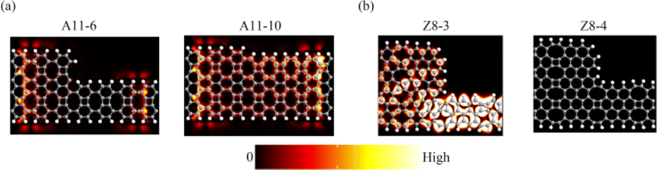 | ||
| Fig. 5 (a) Transport states of A11-6 and A11-10 nanodevices under zero bias voltage. (b) The transport states of Z8-3 and Z8-4 nanodevices under zero bias voltage. | ||
4. Conclusion
In summary, we utilized a combination of DFT and NEGF methods to systematically analyze the electronic properties of 2D nanosheets and 1D nanoribbons, as well as the transport characteristics of the asymmetric controlled net-graphene armchair and zigzag devices. The results indicate that 2D nanosheets of biphenylene, graphene+, net-graphene, and T-graphene all exhibit metallic properties. In addition, graphene+ and T-graphene exhibit isotropy, while biphenylene and net-graphene exhibit anisotropy behaviors. Among the eight constructed 1D new carbon based nanoribbons, except for some of biphenylene and net-graphene nanoribbons exhibit semiconductor properties, all other nanoribbons have energy bands that pass through the Fermi level, exhibiting metallic properties. As the width changes, both biphenylene and net-graphene nanoribbons undergo a transition between metallic and semiconductor properties. The above results indicate that biphenylene and net-graphene materials are multifunctional materials with significant application prospects in the design of new carbon based nanodevices. In addition, in the asymmetric regulation of A11-p and Z8-q nanodevices, A11-10 exhibits excellent conductivity, reaching a maximum value of 53.97 μA at 1.6 V. Moreover, both A11-p and Z8-q nanodevices exhibit certain NDR effects. According to the transmission characteristics of A11-p and Z8-q nanodevices, the new carbon based nanoribbons could be very useful for designing electronic devices by changing the widths.Author contributions
WenSheng Zhou: formal analysis, methodology, writing – original draft. Cheng Luo: formal analysis, methodology, writing – original draft. Yun Chao: project administration, reviewed and edited the manuscript. Songbo Xiong: formal analysis, software. Xianbo Xiao: software, funding acquisition. Tong Chen: technical guidance, writing – review & editing, supervision.Conflicts of interest
There are no conflicts to declare.Acknowledgements
We acknowledge the support from the National Natural Science Foundation of China (Grant No. 62101221 and 12164021), the Natural Science Foundation of Jiangxi Province (Grant No. 20232ACB211008, 20224BAB201022 and 20212ACB201005), and the Program of Qing Jiang Excellent Young Talents, Jiangxi University of Science and Technology (Grant No. JXUSTQJYX201805), the open project of State Key Laboratory of Applied Surface Physics of Fudan University (F202208), and the Postgraduate innovation special fund project, Jiangxi University of Science and Technology (Grant No. XY2022-S210, XY2023-S224).Notes and references
- K. S. Novoselov, A. K. Geim, S. V. Morozov, D. Jiang, Y. Zhang, S. V. Dubonos, I. V. Grigorieva and A. A. Firsov, Electric field effect in atomically thin carbon films, Science, 2004, 306, 666–669 CrossRef CAS PubMed.
- S. Ghosh, I. Calizo, D. Teweldebrhan, E. P. Pokatilov, D. L. Nika, A. A. Balandin, W. Bao, F. Miao and C. N. Lau, Extremely high thermal conductivity of graphene: Prospects for thermal management applications in nanoelectronic circuits, Appl. Phys. Lett., 2008, 92, 151911 CrossRef.
- C. Jia, A. Migliore, N. Xin, S. Huang, J. Wang, Q. Yang, S. Wang, H. Chen, D. Wang, B. Feng, Z. Liu, G. Zhang, D. Qu, H. Tian, M. A. Ratner, H. Q. Xu, A. Nitzan and X. Guo, Covalently bonded single-molecule junctions with stable and reversible photoswitched conductivity, Science, 2016, 352, 1443–1445 CrossRef CAS PubMed.
- V. Palermo, I. A. Kinloch, S. Ligi and N. M. Pugno, Nanoscale mechanics of graphene and graphene oxide in composites: a scientific and technological perspective, Adv. Mater., 2016, 28, 6232–6238 CrossRef CAS PubMed.
- F. Zhao, Y. Liang, H. Cheng, L. Jiang and L. Qu, Highly efficient moisture-enabled electricity generation from graphene oxide frameworks, Energy Environ., 2016, 9, 912–916 RSC.
- S. Chen, Z. Han, M. M. Elahi, K. M. M. Habib, L. Wang, B. Wen, Y. Gao, T. Taniguchi, K. Watanabe, J. Hone, A. W. Ghosh and C. R. Dean, Electron optics with p–n junctions in ballistic graphene, Science, 2016, 353, 1522–1525 CrossRef CAS PubMed.
- F. Peymanirad, S. Kumar Singh, H. Ghorbanfekr-Kalashami, K. S. Novoselov, F. M. Peeters and M. Neek-Amal, Thermal activated rotation of graphene flake on graphene, 2D Materials, 2017, 4, 025015 CrossRef.
- X.-K. Chen and K.-Q. Chen, Thermal transport of carbon nanomaterials, J. Phys.: Condens.Matter, 2020, 32, 153002 CrossRef CAS PubMed.
- L. Yu, X. Tao, S. Feng, L. Tao, L. Zhang, G. Zhao and G. Zhu, Auxiliary ball milling to prepare WS2/graphene nanosheets composite for lithium-ion battery anode materials, Tungsten, 2023, 6, 124–133 Search PubMed.
- S. Yang, Y. Ling, Q. Wu, H. Zhang, Z. Yan, G. Huang, J. Lin and C. Wan, Lignin-derived Porous Graphene for Wearable and Ultrasensitive Strain Sensors, J. Mater. Chem. C, 2022, 10, 11730–11738 RSC.
- Y. Liu, Z. Xu, J. Zhan, P. Li and C. Gao, Superb Electrically Conductive Graphene Fibers via Doping Strategy, Adv. Mater., 2016, 28, 7941–7947 CrossRef CAS PubMed.
- C. Yan, J. Wang and P. S. Lee, Stretchable graphene thermistor with tunable thermal index, ACS Nano, 2015, 9, 2130–2137 CrossRef CAS PubMed.
- X. K. Chen, E. M. Zhang, D. Wu and K. Q. Chen, Strain-Induced Medium-Temperature Thermoelectric Performance of Cu4TiSe4: The Role of Four-Phonon Scattering, Phys. Rev. Appl., 2023, 19, 044052 CrossRef CAS.
- T. Chen, L. Xu, Q. Li and M. Long, Modulation of Electronic Behaviors of InSe Nanosheet and Nanoribbons: The First-Principles Study, Adv. Theory Simul., 2019, 2, 1900099 CrossRef.
- I. S. Osborne, Controlling quantum defects in graphene, Science, 2019, 366, 1090–1092 CrossRef.
- A. Khan, B. Nilam, C. Rukhsar, G. Sayali, B. Mandlekar and A. Kadam, A review article based on composite graphene @tungsten oxide thin films for various applications, Tungsten, 2023, 5, 391–418 CrossRef.
- D. Akinwande and D. Kireev, Wearable graphene sensors use ambient light to monitor health, Nature, 2019, 576, 220–221 CrossRef CAS PubMed.
- Y. Liu, X. Dong and P. Chen, Biological and chemical sensors based on graphene materials, Chem. Soc. Rev., 2011, 41, 2283–2307 RSC.
- X. Yu, H. Cheng, M. Zhang, Y. Zhao, L. Qu and G. Shi, Graphene-based smart materials, Nat. Rev. Mater., 2017, 2, 1–13 Search PubMed.
- Y. Liu, X. Duan, Y. Huang and X. Duan, Two-dimensional transistors beyond graphene and TMDCs, Chem. Soc. Rev., 2018, 47, 6388–6409 RSC.
- W. Yang, S. Berthou, X. Lu, Q. Wilmart, A. Denis, M. Rosticher, T. Taniguchi, K. Watanabe, G. Fève, J. Berroir, G. Zhang, C. Voisin, E. Baudin and B. Plaçais, A graphene Zener-Klein transistor cooled by a hyperbolic substrate, Nat. Nanotechnol., 2018, 13, 47–52 CrossRef CAS PubMed.
- F. Schwierz, Electronics: Industry-compatible graphene transistors, Nature, 2011, 472, 41–42 CrossRef CAS PubMed.
- J. Wang, M. Liang, Y. Fang, T. Qiu, J. Zhang and L. Zhi, Rod-Coating: Towards Large-Area Fabrication of Uniform Reduced Graphene Oxide Films for Flexible Touch Screens, Adv. Mater., 2012, 24, 2874–2878 CrossRef CAS PubMed.
- B. Hwang, S. Lim, M. Park and S. M. Han, Neutral plane control by using polymer/graphene flake composites for flexible displays, RSC Adv., 2017, 7, 8186–8191 RSC.
- G. Anagnostopoulos, P.-N. Pappas, Z. Li, I. A. Kinloch, R. J. Young, K. S. Novoselov, Y. C. Lu, N. Pugno, J. Parthenios, C. Galiotis and K. Papagelis, Mechanical Stability of Flexible Graphene-Based Displays, ACS Appl. Mater. Interfaces, 2016, 8, 22605–22614 CrossRef CAS PubMed.
- Aaryashree, S. Biswas, P. Sharma, V. Awasthi, B. S. Sengar, A. K. Das and S. Mukherjee, Photosensitive ZnO-Graphene Quantum Dot Hybrid Nanocomposite for Optoelectronic Applications, ChemistrySelect, 2016, 1, 1503–1509 CrossRef CAS.
- L. Yu, X. Tao, S. Feng, J. Liu, L. Zhang, G. Zhen and G. Zhu, Recent development of three-dimension printed graphene oxide and MXene-based energy storage devices, Tungsten, 2024, 6, 196–211 CrossRef.
- L. M. C. Silva, B. S. Gonçalves, J. de O. Braga, T. C. de Souza, V. G. de Castro, G. G. Silva, G. R. B. S. Lacerda, T. Matencio, T. C. Barbosa, C. M. Viana, M. Houmard and E. H. M. Nunes, Preparation of titania-reduced graphene oxide composite coatings with electro- and photosensitive properties, Surf. Sci. Appl., 2021, 538, 148029 CrossRef CAS.
- Y. Liu, G. Wang, Q. Huang, L. Guo and X. Chen, Structural and electronic properties of T-graphene: a two-dimensional carbon allotrope with tetrarings, Phys. Rev. Lett., 2012, 108, 225505 CrossRef PubMed.
- Q. Fan, L. Yan, M. W. Tripp, O. Krejčí, S. Dimosthenous, S. R. Kachel, M. Chen, A. S. Foster, U. Koert, P. Liljeroth and J. M. Gottfried, Biphenylene network: A nonbenzenoid carbon allotrope, Science, 2021, 372, 852–856 CrossRef CAS PubMed.
- M. Liu, M. Liu, L. She, Z. Zha, J. Pan, S. Li, T. Li, Y. He, Z. Cai, J. Wang, Y. Zheng, X. Qiu and D. Zhong, Graphene-like nanoribbons periodically embedded with four- and eight-membered rings, Nat. Commun., 2017, 8, 14924 CrossRef CAS PubMed.
- A. Bafekry, M. Faraji, M. M. Fadlallah, H. R. Jappor, S. Karbasizadeh, M. Ghergherehchi and D. Gogova, Biphenylene monolayer as a two-dimensional nonbenzenoid carbon allotrope: a first-principles study, J. Phys.: Condens.Matter, 2022, 34, 015001 CrossRef CAS PubMed.
- G. Liu, T. Chen, X. Li, Z. Xu and X. Xiao, Electronic transport in biphenylene network monolayer: Proposals for 2D multifunctional carbon-based nanodevices, Surf. Sci. Appl., 2022, 599, 153993 CrossRef CAS.
- F. Chen, X. Zhang, X. Guan, S. Gao, J. Hao, L. Li, Y. Yuan, C. Zhang, W. Chen and P. Lu, Nitrogen-Doped or Boron-Doped Twin T-Graphene as Advanced and Reversible Hydrogen Storage Media, SSRN Electron. J., 2022, 622, 156895 Search PubMed.
- Q. Li, J. Zhou, G. Liu and X. G. Wan, Extraordinary negative thermal expansion of monolayer biphenylene, Carbon, 2022, 187, 349–353 CrossRef CAS.
- Z. Tong, A. Pecchia, C. Yam, T. Dumitrică and T. Frauenheim, Ultrahigh Electron Thermal Conductivity in T-Graphene, Biphenylene, and Net-Graphene, Adv. Energy Mater., 2022, 12, 2200657 CrossRef CAS.
- L. Yu, A. Chen, X. Wang, H. Wang, Z. Qin and G. Qin, Softened sp2-sp3 bonding network leads to strong anharmonicity and weak hydrodynamics in graphene+, Phys. Rev. B, 2022, 106, 125410 CrossRef CAS.
- L. Yu, Z. Qin, H. Wang, X. Zheng and G. Qin, Half-negative Poisson's ratio in graphene+ with intrinsic Dirac nodal loop, Cell Rep. Phys. Sci., 2022, 3, 100790 CrossRef CAS.
- G. Liu, T. Chen, L. Xu, X. Dong, K. Cen, Y. Zhu, Z. Xu and X. Xiao, Stable Metallicity of Low Dimensional WCrC Derivatives: A First-Principles Study, Adv. Theory Simul., 2021, 4, 2100036 CrossRef CAS.
- T. Chen, C. Guo, Q. Li, L. Xu, L. Wang, M. Long and C. Shuai, High-performance spin rectification in gallium nitride-based molecular junctions with asymmetric edge passivation, J. Appl. Phys., 2018, 124, 215102 CrossRef.
- A. H. Castro Neto, F. Guinea, N. M. R. Peres, K. S. Novoselov and A. K. Geim, The electronic properties of graphene, Rev. Mod. Phys., 2009, 81, 109–162 CrossRef CAS.
- X.-K. Chen, X.-Y. Hu, P. Jia, Z.-X. Xie and J. Liu, Tunable anisotropic thermal transport in porous carbon foams: The role of phonon coupling, Int. J. Mech. Sci., 2021, 206, 106576 CrossRef.
- V. Saraswat, Y. Yamamoto, H. J. Kim, R. M. Jacobberger, K. R. Jinkins, A. J. Way, N. P. Guisinger and M. S. Arnold, Synthesis of Armchair Graphene Nanoribbons on Germanium-on-Silicon, J. Phys. Chem. C, 2019, 123, 18445–18454 CrossRef CAS.
- W. F. da Cunha, L. A. Ribeiro, A. L. de Almeida Fonseca, R. Gargano and G. M. e Silva, Impurity effects on polaron dynamics in graphene nanoribbons, Carbon, 2015, 91, 171–177 CrossRef.
- R. R. Cloke, T. Marangoni, G. D. Nguyen, T. Joshi, D. J. Rizzo, C. Bronner, T. Cao, S. G. Louie, M. F. Crommie and F. R. Fischer, Site-Specific Substitutional Boron Doping of Semiconducting Armchair Graphene Nanoribbons, J. Am. Chem. Soc., 2015, 137, 8872–8875 CrossRef CAS PubMed.
- P. H. de Oliveira Neto and T. Van Voorhis, Dynamics of charge quasiparticles generation in armchair graphene nanoribbons, Carbon, 2018, 132, 352–358 CrossRef.
- L.-T.-D. Nguyen, V.-C. Ngo, T.-L. Thai, D.-T.-N. Phan, T.-A.-D. Nguyen, V.-T. Tran, T.-T. Vu and T.-K.-L. Phan, Correlation between energy band transition and optical absorption spectrum in bilayer armchair graphene nanoribbons, J. Phys.: Condens.Matter, 2023, 35, 385301 CrossRef PubMed.
- P. Ruffieux, S. Wang, B. Yang, C. Sanchez, J. Liu, T. Dienel, L. Talirz, P. Shinde, C. A. Pignedoli, D. Passerone, T. Dumslaff, X. Feng, K. Muellen and R. Fasel, On-surface synthesis of graphene nanoribbons with zigzag edge topology, Nature, 2016, 531, 489–492 CrossRef CAS PubMed.
- D. Wang, D.-L. Bao, Q. Zheng, C.-T. Wang, S. Wang, P. Fan, S. Mishra, L. Tao, Y. Xiao, L. Huang, X. Feng, K. Müllen, Y.-Y. Zhang, R. Fasel, P. Ruffieux, S. Du and H.-J. Gao, Twisted bilayer zigzag-graphene nanoribbon junctions with tunable edge states, Nat. Commun., 2023, 14, 1018 CrossRef CAS PubMed.
- R. Blackwell, F. Zhao, E. F. Brooks, J. Zhu, I. Piskun, S. Wang, A. Delgado, Y.-L. Lee, S. G. Louie and F. R. Fischer, Spin Splitting of Dopant Edge States in Magnetic Zigzag Graphene Nanoribbons, Nature, 2021, 600, 647–652 CrossRef CAS PubMed.
- G. Z. Magda, X. Jin, I. Hagymási, P. Vancsó, Z. Osváth, P. Nemes-Incze, C. Hwang, L. P. Biró and L. Tapasztó, Room-temperature magnetic order on zigzag edges of narrow graphene nanoribbons, Nature, 2014, 514, 608–611 CrossRef CAS PubMed.
- D. Wang, D.-L. Bao, Q. Zheng, C.-T. Wang, S. Wang, P. Fan, S. Mishra, L. Tao, Y. Xiao, L. Huang, X. Feng, K. Müllen, Y.-Y. Zhang, R. Fasel, P. Ruffieux, S. Du and H.-J. Gao, Twisted bilayer zigzag-graphene nanoribbon junctions with tunable edge states, Nat. Commun., 2023, 14, 1018 CrossRef CAS PubMed.
- J. Taylor, H. Guo and J. Wang, Ab initio modeling of quantum transport properties of molecular electronic devices, Phys. Rev. B: Condens. Matter Mater. Phys., 2001, 63, 245407 CrossRef.
- M. Brandbyge, J.-L. Mozos, P. Ordejón, J. Taylor and K. Stokbro, Density-functional method for nonequilibrium electron transport, Phys. Rev. B: Condens. Matter Mater. Phys., 2002, 65, 165401 CrossRef.
- J. M. Soler, E. Artacho, J. D. Gale, A. García, J. Junquera, P. Ordejón and D. Sánchez-Portal, The SIESTA method for ab initio order-N materials simulation, J. Phys.: Condens.Matter, 2002, 14, 2745–2779 CrossRef CAS.
- A. Bafekry, M. Faraji, M. M. Fadlallah, H. R. Jappor, S. Karbasizadeh, M. Ghergherehchi and D. Gogova, Biphenylene monolayer as a two-dimensional nonbenzenoid carbon allotrope: a first-principles study, J. Phys.: Condens.Matter, 2022, 34, 015001 CrossRef CAS PubMed.
- J. Bai and Y. Huang, Fabrication and electrical properties of graphene nanoribbons, Mater. Sci. Eng., R, 2010, 70, 341–353 CrossRef.
- H. Sun, J. Deng, L. Qiu, X. Fang and H. Peng, Recent progress in solar cells based on one-dimensional nanomaterials, Environ. Sci., 2015, 8, 1139–1159 CAS.
- L. Jiao, L. Zhang, X. Wang, G. Diankov and H. Dai, Narrow graphene nanoribbons from carbon nanotubes, Nature, 2009, 458, 877–880 CrossRef CAS PubMed.
- H. Wang, H. S. Wang, C. Ma, L. Chen, C. Jiang, C. Chen, X. Xie, A.-P. Li and X. Wang, Graphene nanoribbons for quantum electronics, Nat. Rev. Phys., 2021, 3, 791–802 CrossRef CAS.
- M. Slota, A. Keerthi, W. K. Myers, E. Tretyakov, M. Baumgarten, A. Ardavan, H. Sadeghi, C. J. Lambert, A. Narita, K. Müllen and L. Bogani, Magnetic edge states and coherent manipulation of graphene nanoribbons, Nature, 2018, 557, 691–695 CrossRef CAS PubMed.
- X. Li, P. Zhou, X. Hu, E. Rivers, K. Watanabe, T. Taniguchi, D. Akinwande, J. S. Friedman and J. A. C. Incorvia, Cascaded Logic Gates Based on High-Performance Ambipolar Dual-Gate WSe2 Thin Film Transistors, Condensed Matter: Mater. Sci., 2023, 2305, 01790 Search PubMed.
- G. Butseraen, A. Ranadive, N. Aparicio, K. R. Amin, A. Juyal, M. Esposito, K. Watanabe, T. Taniguchi, N. Roch, F. Lefloch and J. Renard, A gate-tunable graphene Josephson parametric amplifier, Nat. Nanotechnol., 2022, 17, 1153–1158 CrossRef CAS PubMed.
- J. P. A. de Mendonça, J. P. C. Silva and F. Sato, High-Frequency Oscillator Based on Nano Graphene, Braz. J. Phys., 2019, 49, 488–493 CrossRef.
- J. Gaskell, L. Eaves, K. S. Novoselov, A. Mishchenko, A. K. Geim, T. M. Fromhold and M. T. Greenaway, Graphene-hexagonal boron nitride resonant tunneling diodes as high-frequency oscillators, Appl. Phys. Lett., 2015, 107, 103105 CrossRef.
- M.-L. Yang, Z.-X. Jin, X.-X. Cao, X.-M. Wang, H.-Y. Ma, H.-J. Pang and G.-X. Yang, Polyoxometalates-derived ternary metal oxides electrocatalyst for N2 reduction under ambient conditions, Tungsten, 2023, 1–10 Search PubMed.
Footnotes |
| † Electronic supplementary information (ESI) available. See DOI: https://doi.org/10.1039/d4ra00806e |
| ‡ Wensheng Zhou and Cheng Lou contributed equally to this work. |
| This journal is © The Royal Society of Chemistry 2024 |