DOI:
10.1039/D4RA00767K
(Paper)
RSC Adv., 2024,
14, 4966-4974
Two-dimensional Janus Si2OX (X = S, Se, Te) monolayers as auxetic semiconductors: theoretical prediction
Received
30th January 2024
, Accepted 31st January 2024
First published on 7th February 2024
Abstract
The auxetic materials have exotic mechanical properties compared to conventional materials, such as higher indentation resistance, more superior sound absorption performance. Although the auxetic behavior has also been observed in two-dimensional (2D) nanomaterials, to date there has not been much research on auxetic materials in the vertical asymmetric Janus 2D layered structures. In this paper, we explore the mechanical, electronic, and transport characteristics of Janus Si2OX (X = S, Se, Te) monolayers by first-principle calculations. Except for the Si2OTe monolayer, both Si2OS and Si2OSe are found to be stable. Most importantly, both Si2OS and Si2OSe monolayers are predicted to be auxetic semiconductors with a large negative Poisson's ratio. The auxetic behavior is clearly observed in the Janus Si2OS monolayer with an extremely large negative Poisson's ratio of −0.234 in the x axis. At the equilibrium state, both Si2OS and Si2OSe materials exhibit indirect semiconducting characteristics and their band gaps can be easily altered by the mechanical strain. More interestingly, the indirect–direct bandgap phase transitions are observed in both Si2OS and Si2OSe monolayers when the biaxial strains are introduced. Further, the studied Janus structures also exhibit remarkably high electron mobility, particularly along the x direction. Our findings demonstrate that Si2OS and Si2OSe monolayers are new auxetic materials with asymmetric structures and show their great promise in electronic and nanomechanical applications.
1 Introduction
The auxetic material is a material possessing a negative Poisson's ratio (NPR). The material contracts laterally when compressed and expands laterally when stretched. NPR has been observed in both bulk and low-dimensional materials. For example, perovskite,1 honeycombs,2 ceramics,3 and cubic metals4 are bulk materials possessing the NPR phenomena. NPR has been also found in one-dimensional (1D) structures.5,6 Particularly, both normal and auxetic behaviors coexist in 1D poly[5]asterane.7 Recently, the auxetic effects have also been revealed in two-dimensional (2D) structures. Black phosphorus is the first 2D material reported to have an NPR with a small value of −0.027.8 Later, the auxetic behavior has also been found in other 2D layered nanomaterials such as borophene,9 Be5C2,10 h-BN,11 and 1T phase of transition metal dichalcogenides.12 In parallel with the bulk and 2D materials, the auxetic effect is also explored in van der Waals superlattices.13 The graphene/hexagonal-BN superlattice has an NPR with values of −0.109 and −0.111 depending on its atomic stacking configuration.13 The origin of auxetic phenomena is found to be the structure of the material. It can be explained by the wrinkled or re-entrant crystal structure. The auxetic materials have exotic mechanical properties compared to conventional materials, such as higher indentation resistance,14 more superior sound absorption performance.15 Therefore, NPR materials have application prospects in the fields of industry,16 biomedicine,17 and sensors.18
Up to now, the variety and application prospects of 2D materials have been extensively demonstrated.19–21 Among them, the SiS monolayer is a typical compound for 2D structures with extraordinary physical characteristics. Particularly, 2D SiS layers can be stable in different polymorphs, including Pma2-SiS, Pmma-SiS, and silicene sulfide.22 The SiS monolayer was found to exhibit mechanical, energetic, and thermal stability.23 Besides, the SiS monolayer possesses excellent mechanical and electronic properties. The SiS exhibits semiconducting features with a tunable direct energy gap and directionally anisotropic carrier mobility. The mobility of electrons in the SiS structure is superior with a value of 1.11 × 104 cm2 V−1 s−1. Most importantly, SiS exhibits high NPR with a value of −0.19 in the x axis.23 Therefore, the SiS monolayer has great promise in applications for nanomechanics and optoelectronics.23
Since the experimental synthesis of 2D vertically asymmetric MoSSe sheet,24,25 2D Janus structures have become an important object in the studies in the material science field.26–29 The 2D Janus monolayers exhibit many exotic physical properties compared to their original symmetric counterparts.30–34 Recently, a few works have presented a particularly intriguing property of the Janus structures, namely the auxetic behavior. The Poisson's ratio with a negative value has been found in both in-plane directions. For example, the Si2SSe monolayer has NPR with a value of −0.11 (−0.08) along the x (y) axis.23 In term of Si2XY (X/Y = S, Se, Te) structures, NPR values lie between −0.062 and −0.113 (−0.082 and −0.122) along the x (y) axis.35 However, little research on the NPR effect has been performed on asymmetric Janus structures. Therefore, the search for Janus structures with auxetic behavior is very important. Motivated by these problems, we report the mechanical features, electronic characteristics, and carrier mobility of Janus 2D Si2OX (X = S, Se, Te) monolayers using density functional theory (DFT) method. It is demonstrated that the Si2OX monolayers, except for Si2OTe, are semiconductors with stable structures, high carrier mobility, and strain-controlled band gap. Most importantly, the NPR phenomena are explored in the Janus Si2OX monolayers. With these findings, we hope to provide fundamental insights and promote extensive studies for Janus structures as well as auxetic materials.
2 Theoretical model and computational details
Our first-principles simulations were carried out based on DFT technique by using the Vienna ab initio simulation package.36,37 We used the projector augmented wave (PAW) method to investigate the core-electron interactions.36 Generalized gradient approximation (GGA) parameterized by Perdew, Burke, and Ernzerhof (PBE)38 was performed for the crystal structure optimizations. Dipole correction is included to treat the errors induced by the periodic boundary condition.39 The Brillouin zone of the studied structures was sampled with a 15 × 15 × 1 k-mesh by Monkhorst–Pack technique.40 The GGA-PBE functional was used for the optimization of the crystal structures. The crystal structures were totally relaxed until the Hellman–Feynman force was less than 1 × 10⁻³ eV Å−1 and the total energy was converged to 10−8 eV. An energy cut-off of 500 eV was selected for the plane-wave basis functions. The GGA-PBE method was used to describe the electron exchange–correlation interaction. Also, the hybrid functional by Heyd–Scuseria–Ernzerhof (HSE06) was used to correct the band gap errors of the considered structures.41 The van der Waals corrections were treated by using the DFT-D3 method suggested by Grimme.42 To avoid the periodic interactions in the vertical direction, we inserted a vacuum distance of 20 Å along the z axis. The phonon spectra of the studied materials were calculated by using the PHONOPY code43 based on the finite displacement technique. The ab initio molecular dynamics (AIMD) simulations with the NVT ensemble (the number of particles N, the calculated cell volume V, and temperature T were fixed) were used to investigate the thermodynamic stabilities of the considered materials.44 The deformation potential (DP) method was adopted to compute the carrier mobilities.45
3 Results and discussion
3.1 Crystal structure, stability, and mechanical characteristics
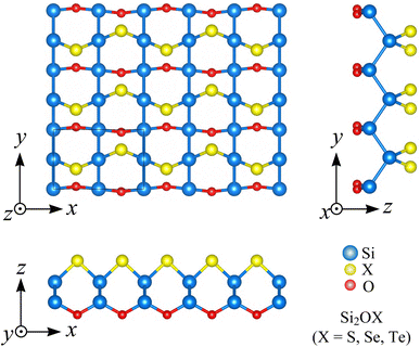
The crystal structures of the vertical asymmetric Janus Si2OX (X = S, Se, and Te) monolayer are shown in Fig. 1. The Janus Si2OX monolayers belong to Pma2 symmetry. We can construct the Janus Si2OX from the Pma2-SiX monolayer22 by substituting the bottom chalcogen layer X with the oxygen layer as presented in Fig. 1. We can see that the unit cell of the Si2OX monolayers contains 8 atoms, including four Si, two O, and two X atoms, as shown in Fig. 1(a). It is found that Janus Si2OX monolayers possess an anisotropic crystal structure. The lattice constants a(b) of Si2OS, Si2OSe, and Si2OTe are calculated to be 5.92(3.90), 5.92(3.92), and 5.97(4.03) Å, respectively. It is shown that there is no significant different in bond angle φ∠Si–O–Si between the structures. Meanwhile, the large different in φ∠Si–X–Si between the structures is found. The obtained φ∠Si–X–Si is found to be 87.82°, 80.37°, and 72.23° for Si2OS, Si2OSe, and Si2OTe, respectively. We present the structural parameters of Si2OX in Table 1.
 |
| | Fig. 1 Optimized crystal structures of Si2OX monolayer in different views. The unitcell is denoted by the rectangle in the top view image. | |
Table 1 Optimized lattice constants a and b, chemical bond lengths d, bond angle ϕ, and elastic constants Cij of Janus Si2OX systems. Since the Janus Si2OTe is unstable, the calculations for Cij of Si2OTe is excluded
| |
a (Å) |
b (Å) |
dSi–O (Å) |
dSi–X (Å) |
dSi–Si (Å) |
φ∠Si–O–Si (°) |
φ∠Si–X–Si (°) |
C11 (N m−1) |
C12 (N m−1) |
C22 (N m−1) |
C66 (N m−1) |
| Si2OS |
5.92 |
3.90 |
1.71 |
2.13 |
2.36 |
120.29 |
87.82 |
92.34 |
−14.56 |
62.75 |
14.70 |
| Si2OSe |
5.92 |
3.92 |
1.71 |
2.29 |
2.36 |
120.22 |
80.37 |
94.48 |
−5.79 |
69.99 |
18.00 |
| Si2SeTe |
5.97 |
4.03 |
1.71 |
2.53 |
2.38 |
120.35 |
72.23 |
— |
— |
— |
— |
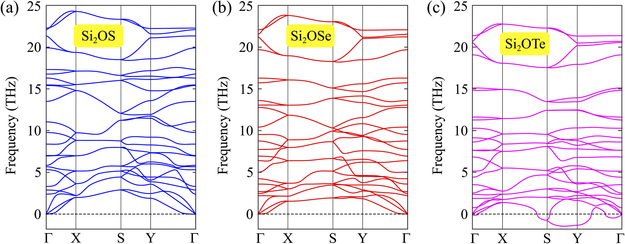
To demonstrate the stability under normal conditions of Si2OX materials, we examine their phonon dispersions. Fig. 2 presents the phonon spectra of three Si2OX monolayers in the first Brillouin zone. Since the unitcell of Si2OX contains 8 atoms, there are 24 vibrational branches within their vibrational spectra. It can be found that there are three acoustic and 21 optical vibrational branches in the phonon dispersion. Besides, the frequencies of the vibrational branches of the two Janus Si2OS and Si2OSe are positive, while the negative frequencies are found in the vibrational spectrum of Si2OTe as revealed in Fig. 2(c). Once the phonon dispersions contain the negative frequencies, the restoring forces against the displacement of the atoms are suppressed. As a consequence, the crystal structure of these materials is unstable. It implies that two monolayers Si2OS and Si2OSe are dynamically stable, while the Janus Si2OTe monolayer is unstable. Therefore, from here on, we only examine Si2OS and Si2OSe and exclude Si2OTe from the calculations due to its structural instability.
 |
| | Fig. 2 Phonon dispersions along the Γ-X-S-Y-Γ high-symmetry line of Si2OS (a), Si2OSe (b), and Si2OTe (c). | |
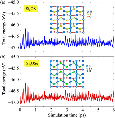
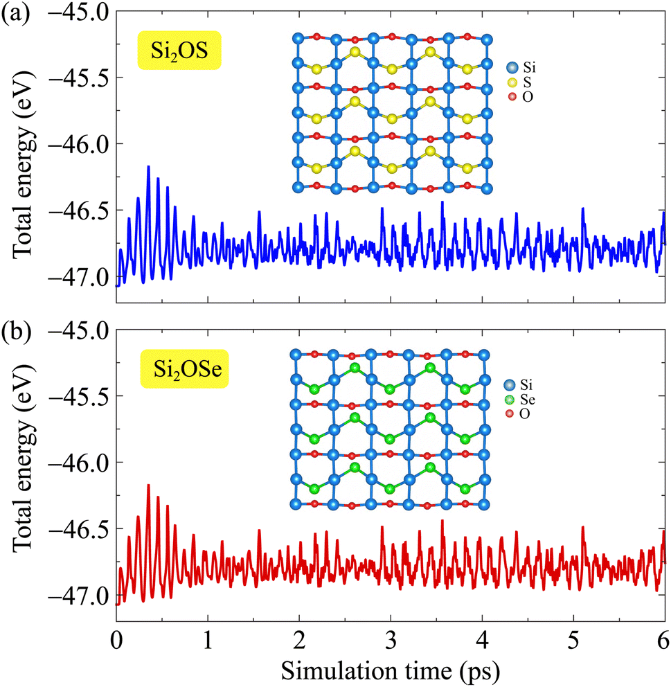
Next, the thermal stability of these two monolayers is also investigated through the AIMD simulation. We perform the AIMD test within 6 ps (each step of 1 fs) at room temperature (300 K). The total energy fluctuations of Si2OS and Si2OSe as functions of simulation time are illustrated in Fig. 3. It is obvious that the total energies fluctuate only by a very small value. The atomic structures of the two monolayers are only slightly deformed and remain structurally solid. Neither the structural phase transitions nor the breaking of chemical bonds were found after the AIMD simulation. It suggests that both Si2OS and Si2OSe are thermodynamic stable at ambient temperature.
 |
| | Fig. 3 AIMD calculations of Si2OS (a) and Si2OSe (b) systems. Inset presents the crystal structure at the end of the simulation progress. | |
Further, we also evaluate the mechanical stabilities of Janus Si2OS and Si2OSe monolayers based on the analysis their elastic characteristics. We calculate the elastic constants of 2D materials, namely C11, C12, C22, and C66, by using Duerloo's method.46 Two in-plane directions of the Janus systems are subjected to small uniaxial strains from −1.5% to 1.5%. At the specified strain, the positions of atoms are re-optimized and the strain-dependence of the energy is found. The calculated energies are polynomial fitted, which yields the in-plane stiffness coefficients. The in-plane stiffness coefficients of 2D Janus Si2OS are found to be C11 = 92.34 N m−1 and C22 = 62.75 N m−1, which are close to those of Si2OSe being C11 = 94.48 N m−1 and C22 = 69.99 N m−1, respectively. Particularly, both Si2OS and Si2OSe monolayers possess a negative value for elastic constant C12 (C12 = −14.56 N m−1 for Si2OS and C12 = −5.79 N m−1 for Si2OSe), suggesting that unusual NPR may occur in these investigated monolayers.47,48 From the obtained elastic constants as listed in Table 1, it is revealed that Cij of both Si2OS and Si2OSe monolayers satisfy the criteria proposed by Born for mechanical stabilities for 2D materials.48,49 This indicates that the mechanical stability of Si2OS and Si2OSe is confirmed.
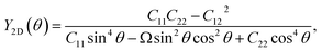
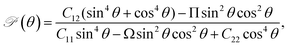
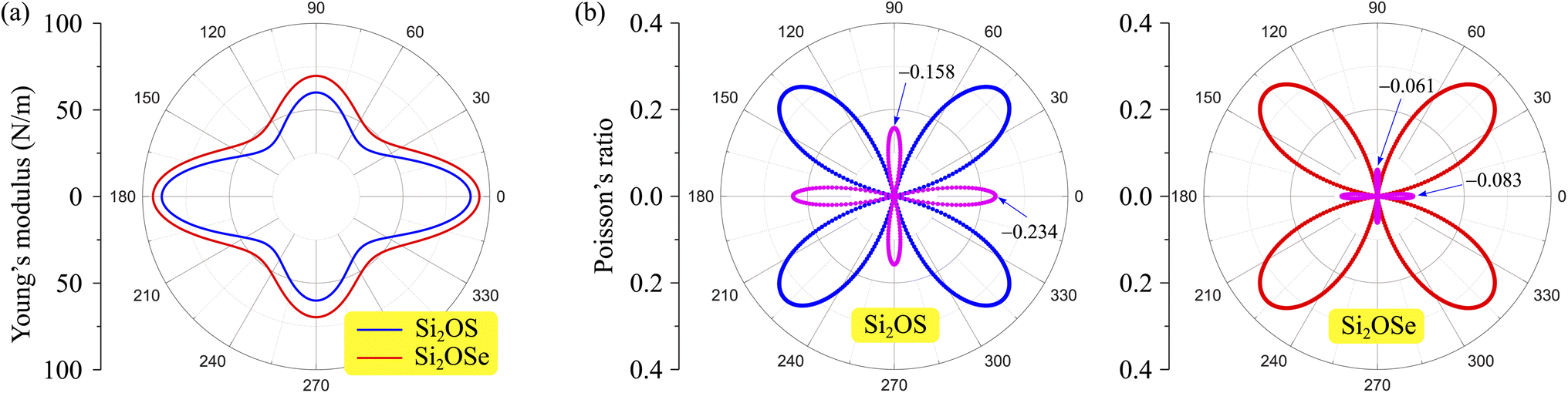
Next, we investigate the mechanical characteristics of Si2OS and Si2OSe through the calculations for Young's modulus and Poisson's ratio. The angular-dependent Young's modulus Y2D(θ) and Poisson's ratio  of the studied materials can be written by the following expressions:50,51
| |
 | (1) |
| |
 | (2) |
where
Ω = 2
C12 − (
C11C22 −
C122)/
C66, Π =
C11 +
C22 − (
C11C22 −
C122)/
C66, and
θ is the angle between the studied direction and the
x-axis.
The angular-dependence of Young's modulus of the studied structures is depicted as shown in Fig. 4(a). Our calculated results revealed that Y2D of Si2OS and Si2OSe monolayers are greatly directionally anisotropic. This is attributed to the in-plane asymmetric geometric structure of the Janus Si2OX systems. The Si2OSe monolayer has a larger Young's modulus value than that of Si2OS monolayer. Young's modulus has the maximum value of 94.00 N m−1 (88.94 N m−1) at θ = 0°, and the minimum value of 48.35 N m−1 (39.28 N m−1) at θ = 48° for the Janus Si2OSe (Si2OS) compound, respectively. Possessing a small Y2D, Si2OS and Si2OSe monolayers have high mechanical flexibility compared to other 2D structures, such as graphene (344 N m−1),52 binary MoS2 compound (130 N m−1)53 or Janus ternary MoSSe monolayer (113 N m−1).54
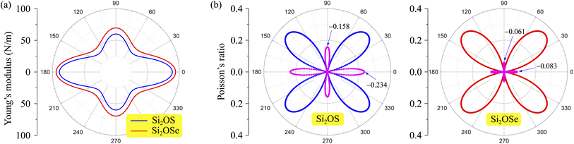 |
| | Fig. 4 (a) Young's modulus Y2D(θ) and (b) Poisson's ratio  of Janus Si2OS and Si2OSe structures. Pink symbols in (b) indicate the negative values of of Janus Si2OS and Si2OSe structures. Pink symbols in (b) indicate the negative values of  | |
In Fig. 4(b), we reveal the calculated polar diagrams of Poisson's ratio  of Janus Si2OS and Si2OSe monolayers. It is found that Si2OS and Si2OSe monolayers exhibit a high anisotropy. Remarkably, the negative Poisson's ratio is found in both Si2OS and Si2OSe compounds. This is consistent with the expectation above that these structures have a negative C12. The NPR feature can be seen in both x and y axes as depicted in Fig. 4(b). The calculated results demonstrate that Janus Si2OS has a large in-plane NPR, up to −0.234 and −0.158 in the x and y axes, respectively. Surprisingly, these NPR values are much larger than those of SiS (−0.19 and −0.10)48 and Janus Si2SSe (−0.131 and −0.122 in the x and y axes, respectively).35 The NPR values of Si2OSe monolayer are found to be −0.083 (−0.061) in the x(y) axis as presented in Fig. 4(b). The appearance of the NPR confirms that Janus Si2OS and Si2OSe can be treated as auxetic semiconductors. Compared with usual nanomaterials, 2D auxetic structures possess many extraordinary physical features with promising application in various fields of nanotechnology.55
3.2 Electronic properties
Here, we report the electronic properties of two stable structures of Si2OX, namely Si2OS and Si2OSe monolayers. First, the band structures of the two compounds are examined by both the PBE and HSE06 methods as shown in Fig. 5. It can be observed that Si2OS and Si2OSe monolayers exhibit indirect semiconducting characteristics. In the case of Si2OS, the conduction band minimum (CBM) and valence band maximum (VBM) are found at the Γ point and on the XΓ line, respectively. Meanwhile, the CBM and VBM of Si2OSe are found respectively at the Y and Γ points. It should be noted that the vertical symmetric SiS and SiSe are direct bandgap semiconductors.22,23 Thus, the symmetry breaking significantly changes the electronic characteristics of Janus structures. At the PBE level, the indirect bandgaps of Si2OS and Si2OSe monolayers are respectively obtained to be 1.35 and 1.20 eV. The bandgap correction by using the HSE06 functional shows that the bandgaps of Si2OS and Si2OSe monolayers are 2.18 and 1.97 eV, respectively. The obtained HSE06 bandgaps of Si2OS and Si2OSe are wider than those of SiS (1.22 eV)23,56 and SiSe (1.44 eV23 and 1.35 eV 56). The obtained bandgaps of Si2OS and Si2OSe monolayers are listed in Table 2.
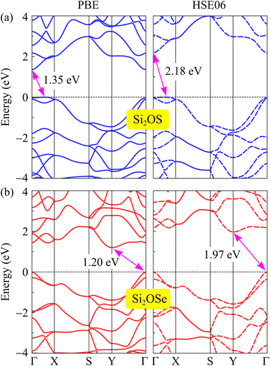 |
| | Fig. 5 The PBE and HSE06 band structures of Si2OS (a) and Si2OSe (b) monolayers. | |
Table 2 Obtained bandgaps Eg using PBE/HSE06 functional, difference between the vacuum levels ΔΦ, and work function on the O(X) side ΦO(ΦX) of Si2OX materials
| |
EPBEg (eV) |
EHSE06g (eV) |
ΔΦ (eV) |
ΦO (eV) |
ΦX (eV) |
| Si2OS |
1.35 |
2.18 |
0.06 |
5.46 |
5.40 |
| Si2OSe |
1.20 |
1.97 |
0.47 |
5.22 |
4.75 |
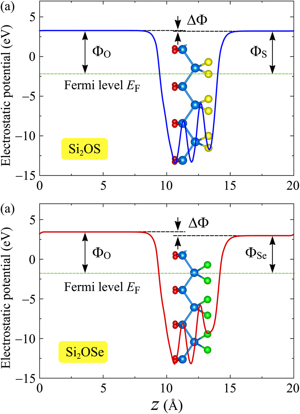
In addition to the electronic band diagrams, the work function is also a fundamental electronic feature of the material that should be taken into account. The work function denotes the required energy for electrons to escape from the surfaces of the studied structures and can be estimated based on the vacuum level Evac and Fermi level EF as: Φ = Evac − EF. We can find the vacuum level based on calculations for the electrostatic potential of the studied structures. An intrinsic electric field exists in the vertical direction of the Janus material due to the electronegativity difference between the two sides of this layered structure. This difference in electronegativity leads to the vacuum level difference between the two sides of materials. As a consequence, there is a work function difference on the two sides of the studied asymmetric structures. Since the electronegativity of O atom is greater than that of the chalcogen atom X, the intrinsic electric field in the Si2OX structures is directed from X to O. In Fig. 6, we show the electrostatic potential energies with a dipole correction of Si2OS and Si2OSe materials. A vacuum level difference ΔΦ is found in both Si2OS and Si2OSe. The larger the difference in atomic size between O and X elements, the larger the value ΔΦ is. The calculated ΔΦ for Si2OS and Si2OSe are 0.06 and 0.47 eV, respectively. Table 2 summarizes our obtained results for ΔΦ and work functions of Si2OS and Si2OSe materials. The work functions of Si2OS are slightly higher than those of Si2OSe. The data in Table 2 reveal that it is easier for electrons to totally escape from the X surface than from the of O surface.
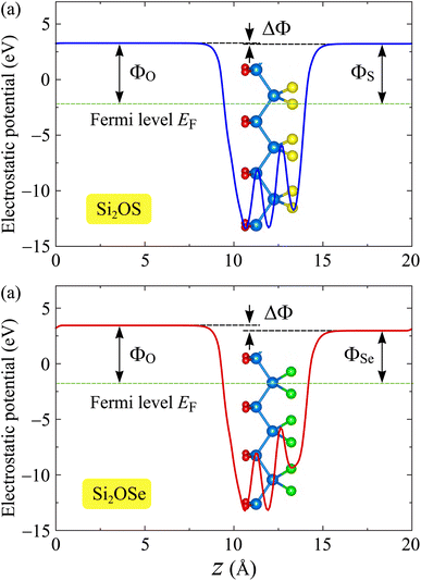 |
| | Fig. 6 Electrostatic potentials of Si2OS (a) and Si2OSe (b) monolayers. | |
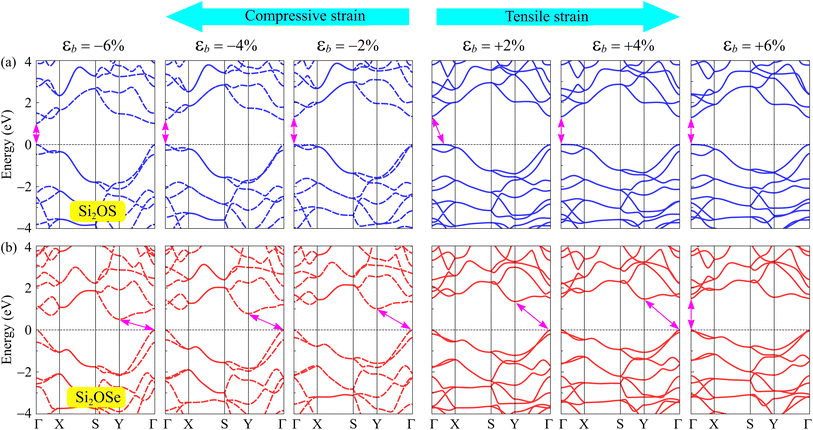
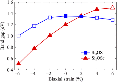
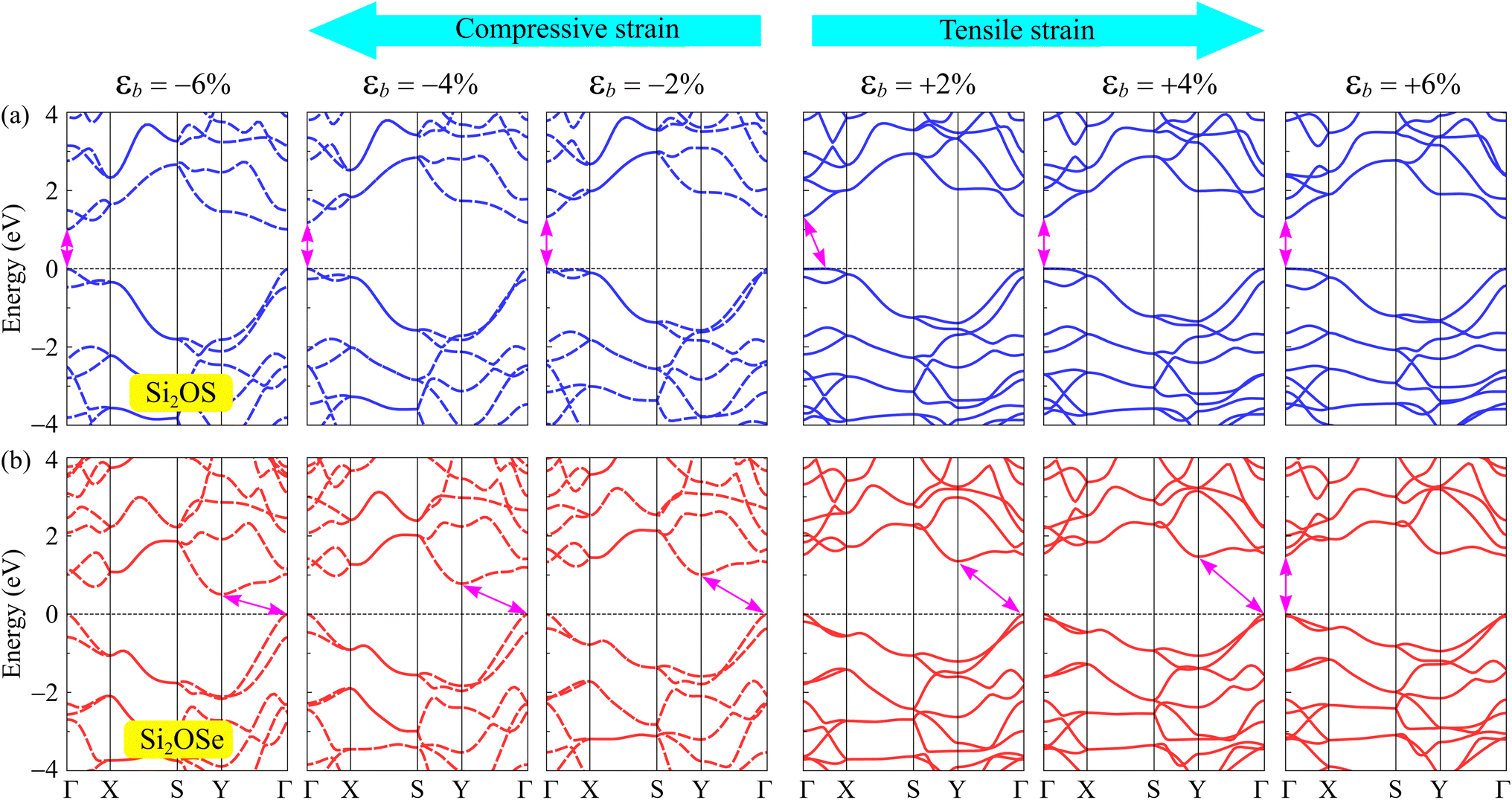
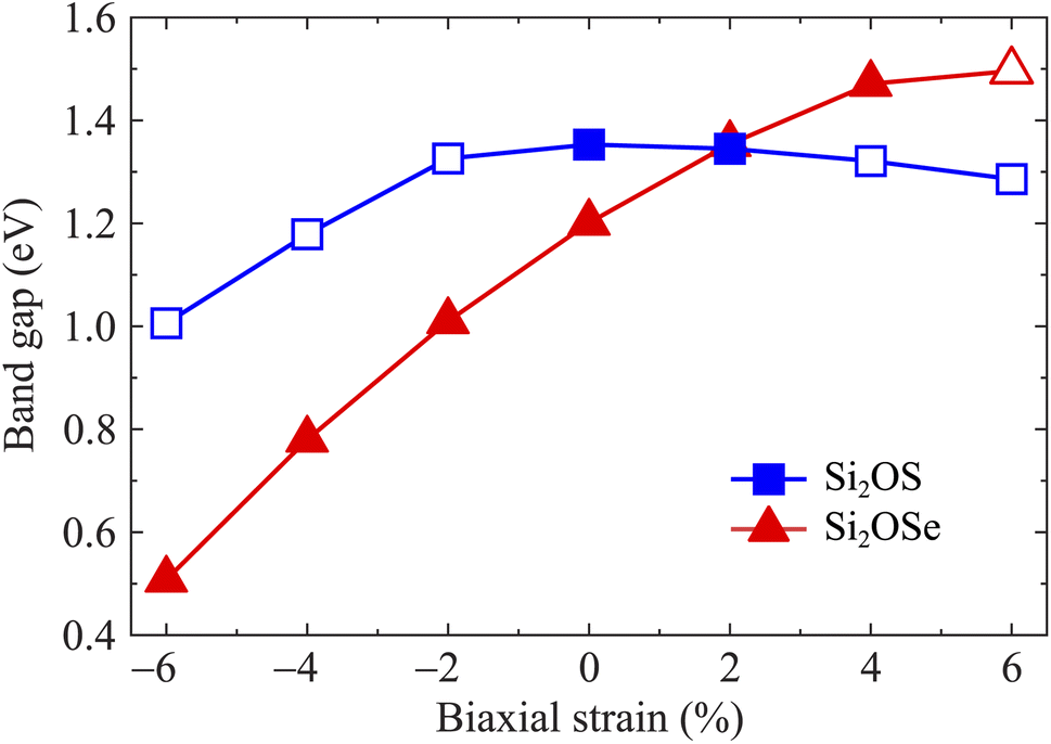
It is well-known that there are many techniques to tune the electronic features of 2D materials, such as chemical functionalization, defect effects, doping, etc. Among these, mechanical strain is an effective and simple approach to control electronic properties.27,31,48 In this paper, a biaxial strain between −6% and 6% is applied to examine the strain-dependence of the electronic features of Si2OS and Si2OSe monolayers. The biaxial strain can be evaluated as εb = (a − a0)/a0, where a0 and a denote the lattice constants of Si2OS and Si2OSe at equilibrium and strained states. Mechanical strains with positive and negative values correspond to tension and compression, respectively. Fig. 7 depicts the band structures of Si2OS and Si2OSe monolayers at several values of εb. We can see that the mechanical strain significantly adjusts the electronic band structures, especially for the Janus Si2OS monolayer. When the tensile strain reaches +4%, the indirect–direct bandgap transition is found in the Si2OS structure as shown in Fig. 7(a). Also, Si2OS is found as direct semiconductor with both VBM and CBM at the Γ point when the tensile strain is introduced. Both tensile and compressive strains shift the band edges in the electronic structure of the Janus structure, leading to a change in the bandgap. Besides, the phase transition from indirect to direct bandgap is also observed in Si2OSe monolayer at εb = 6% and the applied strain significantly modulates its bandgap. Fig. 8 presents the bandgaps of Janus Si2OX structures as functions of εb. As can be seen from Fig. 8, the bandgap of Si2OSe is significantly reduced by compressive strains, whereas tensile strain slightly increases its bandgap. In the case of Si2OS, the biaxial strains reduce its bandgap. However, the effect of εb on the energy gap of Si2OS is quite weak. The maximum bandgap of Si2OS is 1.35 eV at equilibrium (εb = 0) and the lowest is at εb = −6 with the value of 1.01 eV. The strain-induced phase transitions from indirect-to-direct energy gap in both Si2OS and Si2OS make them promising for nanoelectromechanical applications.
 |
| | Fig. 7 The PBE band structures of (a) Si2OS and (b) Si2OSe materials under the biaxial strain εb. | |
 |
| | Fig. 8 Dependence of the bandgaps of Si2OS and Si2OSe on the biaxial strain εb. The filled/empty shapes indicate the indirect/direct bandgaps, respectively. | |
3.3 Carrier mobility
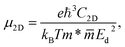
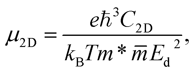
In the following, we compute the carrier mobilities in Janus Si2OS and Si2OXSe materials. Carrier mobility is a key parameter relevant to technological applications such as electronic devices. By employing the deformation potential (DP) approximation,45 the mobilities of electrons and holes in 2D systems can be obtained by the following equation:57| |
 | (3) |
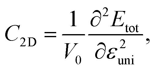
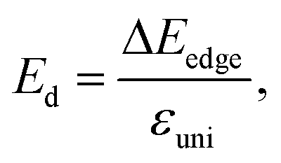
where e, ℏ, kB, and T refer to the elementary charge, the reduced Planck's constant, Boltzmann's constant, and the temperature, respectively. m* and  are respectively the carrier effective mass along the x/y axis and average effective mass. C2D refers to the elastic modulus and Ed indicates the DP constant. Herein, the carrier mobility is calculated at T = 300 K (room temperature). The effective mass of carriers, elastic modulus, and the DP constant are determined as follows:
| |
 | (4) |
| |
 | (5) |
| |
 | (6) |
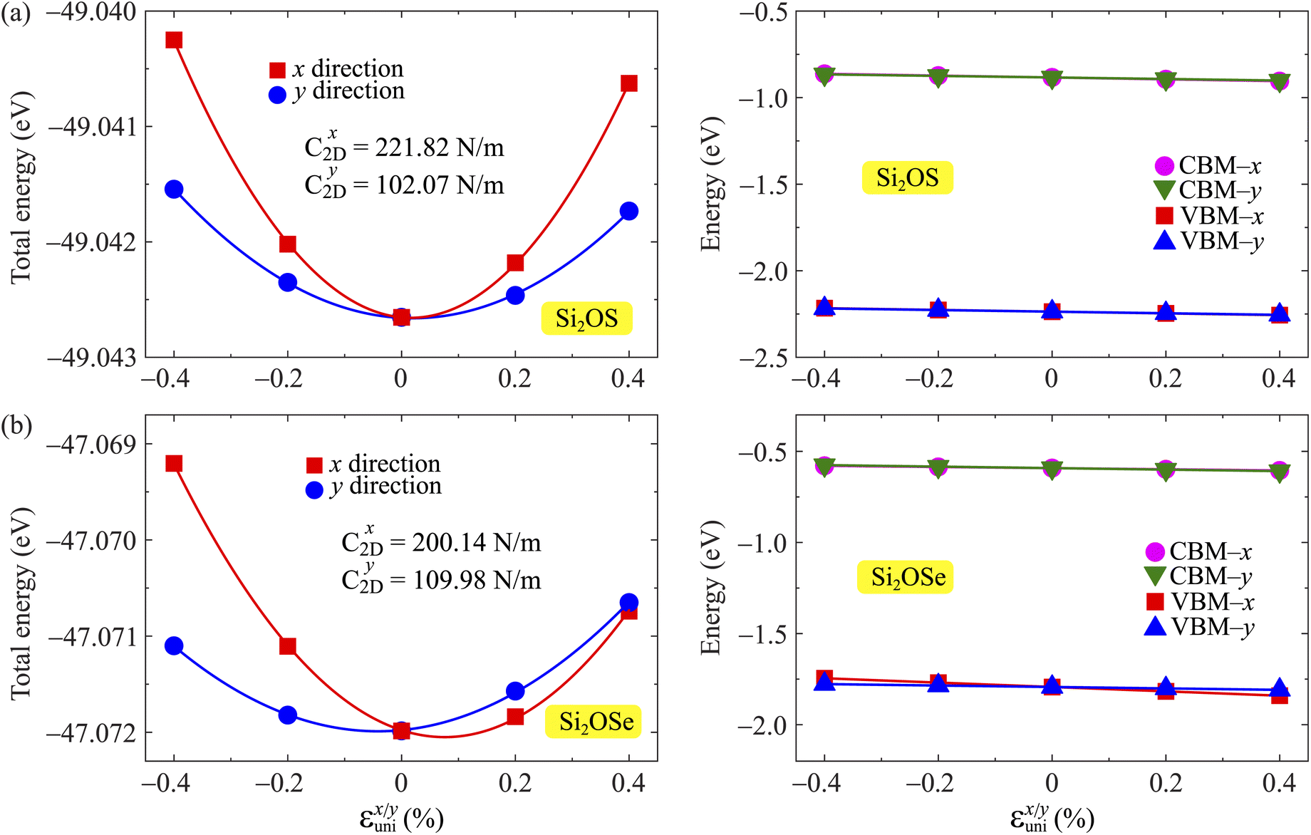
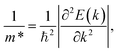
where E(k) indicates the wavenumber k-dependent energy at the VBM for holes and CBM for electrons. V0 and Etot refer to the area of optimized unitcell and the total energy, respectively. εuni is the small uniaxial strain along the x/y axis, which varies between 0 and ± 0.4% in our calculations for the transport parameters. ΔEedge stands for the uniaxial strain-induced energy change of the band edges. The transport parameters C2D and Ed are obtained by fitting the strain-dependence of the total energies and band edges energy as presented in Fig. 9. The total energy depends not only strongly on the strain but also on the direction of the uniaxial strain, namely along the x or y axis. This will cause the elastic modulus of the examined structures to be high and they are high directional anisotropy. Meanwhile, the change in position of the band edges of Si2OS and Si2OSe monolayers in the presence of the applied uniaxial strains along the x and y axes is small, suggesting that the directional isotropy of the DP constant is high.
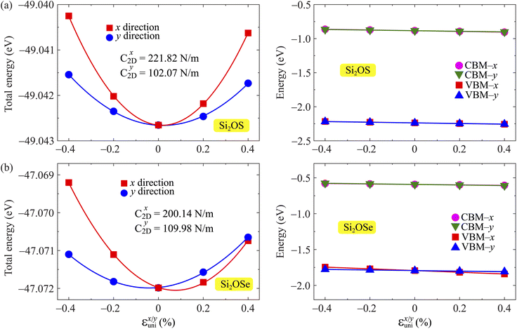 |
| | Fig. 9 The total energy and band-edge energy of Si2OS (a) and Si2OSe (b) monolayers as functions of small uniaxial strains εunix/y. | |
The obtained transport parameters m*, C2D, Ed, and corresponding carrier mobility μ2D along the axes x and y are presented in Table 3. We can see that Janus Si2OS and Si2OXSe exhibit highly directionally anisotropic transport features due their in-plane anisotropic crystal lattice. The results of our calculations indicate that the electrons in Janus Si2OS and Si2OXSe monolayers have low effective mass. The electron effective masses of Si2OS and Si2OXSe along the x(y) directions are respectively 0.48m0 (0.50m0) and 0.59m0 (1.39m0) with m0 being the free electron mass. Since the electrons have a low effective mass, they will respond quickly to the external field, which is expected to result in high electron mobilities in the Janus Si2OS and Si2OXSe monolayers. In Janus Si2OS, the electrons have a smaller effective mass than that of the holes. Meanwhile, the hole effective masses of Si2OSe are smaller than those of the electrons. These results are consistent with the band dispersion as shown in Fig. 5. For example, the band structure of Si2OSe around the VBM is flatter than that around the CBM as presented in Fig. 5(a). The flatter the band structure at the band edge (the larger the curvature radius), the smaller the second derivative ∂2E(k)/∂k,2 leading to a large effective mass.
Table 3 The calculated effective masses of carriers m* (in unit of the mass of a free electron m0), elastic modulus C2D (N m−1), DP constant Ed (eV), and carrier mobility μ2D (cm2 V−1 s−1) along the x/y transport axis of Si2OS and Si2OSe monolayers
| |

|

|
C2Dx |
C2Dy |
Edx |
Edy |
μ2Dx |
μ2Dy |
| Si2OS |
Electron |
0.48 |
0.50 |
221.82 |
102.07 |
−5.25 |
−4.47 |
727.98 |
443.60 |
| Hole |
1.57 |
6.21 |
221.82 |
102.07 |
−4.96 |
−4.65 |
39.12 |
5.17 |
| Si2OSe |
Electron |
0.59 |
1.39 |
200.14 |
109.98 |
−3.21 |
−4.10 |
773.26 |
110.56 |
| Hole |
0.4 |
0.38 |
200.14 |
109.98 |
−11.95 |
−3.96 |
191.16 |
1.01 × 10³ |
Table 3 reveals that electron mobility and hole mobility are both directionally anisotropic. The electron mobility μ2D along the x axis is much higher than that along the y axis for both studied Janus structures. The electron mobilities of Si2OS are calculated to be μ2Dy = 727.98 cm2 V−1 s−1 and μ2Dx = 443.60 cm2 V−1 s−1, which are high enough for applications in nanoelectronic devices.58 The electron mobilities of Si2OS monolayer are comparable with obtained results for Janus Si2SSe μ2Dy = 897.66 cm2 V−1 s−1 and μ2Dx = 627.13 cm2 V−1 s−1.35 The anisotropy in electron mobility is evident in the Si2OSe monolayer, where the electron mobility along x direction μ2Dx is about 7 times higher than μ2Dy. The calculated results for carrier mobility of Janus Si2OS and Si2OXSe monolayers are listed in Table 3. It should also be mentioned that the holes in Si2OXSe have high mobility, up to 1000 cm2 V−1 s−1 along the y axis, which is greater than the electron mobility.
4 Conclusions
Based on DFT calculations, we have reported the structural, mechanical, electronic, and transport features of 2D Janus structures Si2OX (X = S, Se, Te). Our results demonstrated that the Si2OS and Si2OSe monolayers are highly stable structures while Si2OTe monolayer is an unstable structure with large negative frequencies in its phonon spectrum. The auxetic effect has been found in the two investigated stable monolayers with large NPR values. Especially, the Si2OS structure possesses a very high NPR, up to −0.234 in the x-axis. The studied monolayers Si2OS and Si2OSe are both indirect band gap semiconductors and the transitions from indirect to direct band gap have been found in these structures when the biaxial strains are introduced. In addition, carrier mobility in both considered Janus structures is very high and anisotropic. Our findings reveal the novel properties of Janus Si2OX structures and great potential in multifunctional applications.
Conflicts of interest
There are no conflicts to declare.
Acknowledgements
N. A. P acknowledges the support from the Belarusian Republican Foundation for Fundamental Research (Grant No. F23RNF-049) and the Belarusian National Research Program “Convergence-2025”.
References
- C. W. Huang, W. Ren, V. C. Nguyen, Z. Chen, J. Wang, T. Sritharan and L. Chen, Adv. Mater., 2012, 24, 4170–4174 CrossRef CAS PubMed.
- R. Lakes, Science, 1987, 235, 1038–1040 CrossRef CAS PubMed.
- X. Xu, Q. Zhang, M. Hao, Y. Hu, Z. Lin, L. Peng, T. Wang, X. Ren, C. Wang, Z. Zhao, C. Wan, H. Fei, L. Wang, J. Zhu, H. Sun, W. Chen, T. Du, B. Deng, G. J. Cheng, I. Shakir, C. Dames, T. S. Fisher, X. Zhang, H. Li, Y. Huang and X. Duan, Science, 2019, 363, 723–727 CrossRef CAS PubMed.
- F. Milstein and K. Huang, Phys. Rev. B: Condens. Matter Mater. Phys., 1979, 19, 2030–2033 CrossRef CAS.
- J. F. Silveira and A. R. Muniz, Carbon, 2017, 113, 260–265 CrossRef CAS.
- B. Saha and A. Datta, J. Phys. Chem. C, 2018, 122, 19204–19211 CrossRef CAS.
- B. Saha, S. M. Pratik and A. Datta, Chem.–Eur. J., 2017, 23, 12917–12923 CrossRef CAS PubMed.
- J.-W. Jiang and H. S. Park, Nat. Commun., 2014, 5, 4727 CrossRef CAS PubMed.
- A. J. Mannix, X.-F. Zhou, B. Kiraly, J. D. Wood, D. Alducin, B. D. Myers, X. Liu, B. L. Fisher, U. Santiago, J. R. Guest, M. J. Yacaman, A. Ponce, A. R. Oganov, M. C. Hersam and N. P. Guisinger, Science, 2015, 350, 1513–1516 CrossRef CAS PubMed.
- Y. Wang, F. Li, Y. Li and Z. Chen, Nat. Commun., 2016, 7, 11488 CrossRef CAS PubMed.
- S. Woo, H. C. Park and Y.-W. Son, Phys. Rev. B, 2016, 93, 075420 CrossRef.
- L. Yu, Q. Yan and A. Ruzsinszky, Nat. Commun., 2017, 8, 15224 CrossRef CAS PubMed.
- X. Li, X. Qiang, Z. Gong, Y. Zhang, P. Gong and L. Chen, Research, 2021, 2021, 1904839 CAS.
- A. Alderson and K. L. Alderson, Proc. Inst. Mech. Eng., 2007, 221, 565–575 CrossRef CAS.
- W. Yang, Z.-M. Li, W. Shi, B.-H. Xie and M.-B. Yang, J. Mater. Sci., 2004, 39, 3269–3279 CrossRef CAS.
- C. Huang and L. Chen, Adv. Mater., 2016, 28, 8079–8096 CrossRef CAS PubMed.
- F. Scarpa, IEEE Signal Process. Mag., 2008, 25, 126–128 Search PubMed.
- M. Avellaneda and P. J. Swart, J. Acoust. Soc. Am., 1998, 103, 1449–1467 CrossRef CAS.
- T. C. Phong and L. T. T. Phuong, Phys. B, 2023, 666, 415119 CrossRef CAS.
- T. C. Phong, V. T. T. Vi and L. T. T. Phuong, Phys. Lett. A, 2023, 480, 128946 CrossRef CAS.
- T. C. Phong, N. T. Nam and L. T. T. Phuong, Phys. Lett. A, 2023, 474, 128830 CrossRef CAS.
- J.-H. Yang, Y. Zhang, W.-J. Yin, X. G. Gong, B. I. Yakobson and S.-H. Wei, Nano Lett., 2016, 16, 1110–1117 CrossRef CAS PubMed.
- T. Jing, D. Liang, M. Deng and S. Cai, J. Mater. Chem. C, 2020, 8, 10382–10389 RSC.
- A.-Y. Lu, H. Zhu, J. Xiao, C.-P. Chuu, Y. Han, M.-H. Chiu, C.-C. Cheng, C.-W. Yang, K.-H. Wei, Y. Yang, Y. Wang, D. Sokaras, D. Nordlund, P. Yang, D. A. Muller, M.-Y. Chou, X. Zhang and L.-J. Li, Nat. Nanotechnol., 2017, 12, 744 CrossRef CAS PubMed.
- J. Zhang, S. Jia, I. Kholmanov, L. Dong, D. Er, W. Chen, H. Guo, Z. Jin, V. B. Shenoy, L. Shi and J. Lou, ACS Nano, 2017, 11, 8192–8198 CrossRef CAS PubMed.
- T. V. Vu, V. T. T. Vi, H. V. Phuc, A. I. Kartamyshev and N. N. Hieu, Phys. Rev. B, 2021, 104, 115410 CrossRef CAS.
- T. V. Vu, C. V. Nguyen, H. V. Phuc, A. A. Lavrentyev, O. Y. Khyzhun, N. V. Hieu, M. M. Obeid, D. P. Rai, H. D. Tong and N. N. Hieu, Phys. Rev. B, 2021, 103, 085422 CrossRef CAS.
- N. N. Hieu, H. V. Phuc, A. I. Kartamyshev and T. V. Vu, Phys. Rev. B, 2022, 105, 075402 CrossRef CAS.
- T. V. Vu, H. V. Phuc, A. I. Kartamyshev and N. N. Hieu, Appl. Phys. Lett., 2023, 122, 061601 CrossRef CAS.
- T. V. Vu, V. T. T. Vi, C. V. Nguyen, H. V. Phuc and N. N. Hieu, J. Phys. D: Appl. Phys., 2020, 53, 455302 CrossRef CAS.
- T. V. Vu, V. T. T. Vi, H. V. Phuc, C. V. Nguyen, N. A. Poklonski, C. A. Duque, D. P. Rai, B. D. Hoi and N. N. Hieu, J. Phys.: Condens.Matter, 2021, 33, 225503 CrossRef CAS PubMed.
- L. Dong, J. Lou and V. B. Shenoy, ACS Nano, 2017, 11, 8242–8248 CrossRef CAS PubMed.
- A. Mogulkoc, Y. Mogulkoc, S. Jahangirov and E. Durgun, J. Phys. Chem. C, 2019, 123, 29922–29931 CrossRef CAS.
- X. Yan, X. Cui, B. Wang, H. Yan, Y. Cai and Q. Ke, Iscience, 2023, 26, 106731 CrossRef CAS PubMed.
- N. T. Hiep, C. Q. Nguyen and N. N. Hieu, Appl. Phys. Lett., 2023, 123, 092102 CrossRef CAS.
- G. Kresse and J. Furthmüller, Phys. Rev. B: Condens. Matter Mater. Phys., 1996, 54, 11169–11186 CrossRef CAS PubMed.
- G. Kresse and J. Furthmüller, Comput. Mater. Sci., 1996, 6, 15–50 CrossRef CAS.
- J. P. Perdew, K. Burke and M. Ernzerhof, Phys. Rev. Lett., 1996, 77, 3865 CrossRef CAS PubMed.
- J. Neugebauer and M. Scheffler, Phys. Rev. B: Condens. Matter Mater. Phys., 1992, 46, 16067–16080 CrossRef CAS PubMed.
- H. J. Monkhorst and J. D. Pack, Phys. Rev. B: Solid State, 1976, 13, 5188–5192 CrossRef.
- J. Heyd, G. E. Scuseria and M. Ernzerhof, J. Chem. Phys., 2003, 118, 8207 CrossRef CAS.
- S. Grimme, J. Antony, S. Ehrlich and H. Krieg, J. Chem. Phys., 2010, 132, 154104 CrossRef PubMed.
- A. Togo, L. Chaput and I. Tanaka, Phys. Rev. B: Condens. Matter Mater. Phys., 2015, 91, 094306 CrossRef.
- S. Nosé, J. Chem. Phys., 1984, 81, 511 CrossRef.
- J. Bardeen and W. Shockley, Phys. Rev., 1950, 80, 72 CrossRef CAS.
- K.-A. N. Duerloo, M. T. Ong and E. J. Reed, J. Phys. Chem. Lett., 2012, 3, 2871–2876 CrossRef CAS.
- X. Zhou, N. Zhou, C. Li, H. Song, Q. Zhang, X. Hu, L. Gan, H. Li, J. Lü, J. Luo, J. Xiong and T. Zhai, 2D Mater., 2017, 4, 025048 CrossRef.
- T. Jing, D. Liang, M. Deng and S. Cai, J. Mater. Chem. C, 2020, 8, 10382–10389 RSC.
- M. Born and K. Huang, Am. J. Phys., 1955, 23, 474 CrossRef.
- N. T. Hung, A. R. T. Nugraha and R. Saito, J. Phys. D: Appl. Phys., 2018, 51, 075306 CrossRef.
- P. Xiang, S. Sharma, Z. M. Wang, J. Wu and U. Schwingenschlögl, ACS Appl. Mater. Interfaces, 2020, 12, 30731 CrossRef CAS PubMed.
- E. Cadelano, P. L. Palla, S. Giordano and L. Colombo, Phys. Rev. B: Condens. Matter Mater. Phys., 2010, 82, 235414 CrossRef.
- R. C. Cooper, C. Lee, C. A. Marianetti, X. Wei, J. Hone and J. W. Kysar, Phys. Rev. B: Condens. Matter Mater. Phys., 2013, 87, 035423 CrossRef.
- S.-D. Guo, Phys. Chem. Chem. Phys., 2018, 20, 7236–7242 RSC.
- R. Peng, Y. Ma, Z. He, B. Huang, L. Kou and Y. Dai, Nano Lett., 2019, 19, 1227–1233 CrossRef CAS PubMed.
- J.-H. Yang, Q. Yuan, H. Deng, S.-H. Wei and B. I. Yakobson, J. Phys. Chem. C, 2017, 121, 123–128 CrossRef CAS.
- W. Wan, S. Zhao, Y. Ge and Y. Liu, J. Phys.: Condens.Matter, 2019, 31, 435501 CrossRef CAS PubMed.
- B. Radisavljevic, A. Radenovic, J. Brivio, V. Giacometti and A. Kis, Nat. Nanotechnol., 2011, 6, 147–150 CrossRef CAS PubMed.
|
| This journal is © The Royal Society of Chemistry 2024 |
Click here to see how this site uses Cookies. View our privacy policy here. 
 Open Access Article
 This Open Access Article is licensed under a Creative Commons Attribution-Non Commercial 3.0 Unported Licence
 b,
Vo T. T. Vi
b,
Vo T. T. Vi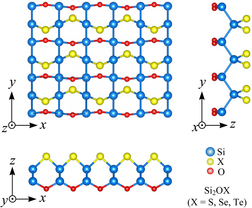
 of the studied materials can be written by the following expressions:50,51

 of Janus Si2OS and Si2OSe structures. Pink symbols in (b) indicate the negative values of
 of Janus Si2OS and Si2OSe monolayers. It is found that Si2OS and Si2OSe monolayers exhibit a high anisotropy. Remarkably, the negative Poisson's ratio is found in both Si2OS and Si2OSe compounds. This is consistent with the expectation above that these structures have a negative C12. The NPR feature can be seen in both x and y axes as depicted in Fig. 4(b). The calculated results demonstrate that Janus Si2OS has a large in-plane NPR, up to −0.234 and −0.158 in the x and y axes, respectively. Surprisingly, these NPR values are much larger than those of SiS (−0.19 and −0.10)48 and Janus Si2SSe (−0.131 and −0.122 in the x and y axes, respectively).35 The NPR values of Si2OSe monolayer are found to be −0.083 (−0.061) in the x(y) axis as presented in Fig. 4(b). The appearance of the NPR confirms that Janus Si2OS and Si2OSe can be treated as auxetic semiconductors. Compared with usual nanomaterials, 2D auxetic structures possess many extraordinary physical features with promising application in various fields of nanotechnology.55
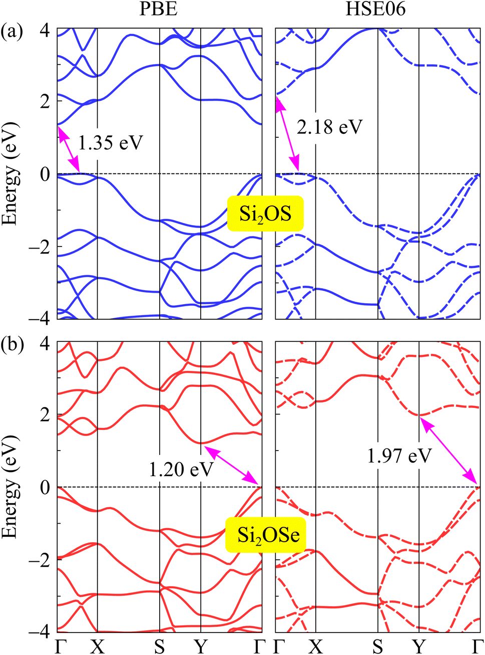
 are respectively the carrier effective mass along the x/y axis and average effective mass. C2D refers to the elastic modulus and Ed indicates the DP constant. Herein, the carrier mobility is calculated at T = 300 K (room temperature). The effective mass of carriers, elastic modulus, and the DP constant are determined as follows: