DOI:
10.1039/D4RA00184B
(Paper)
RSC Adv., 2024,
14, 13618-13627
Improved isoprene detection performance of Si-doped WO3 films deposited by sputtering and post-annealing†
Received
8th January 2024
, Accepted 12th April 2024
First published on 25th April 2024
Abstract
Si-doped WO3 films were sputtered at room temperature and then annealed in air at 500 °C. The Si doping resulted in structural distortion from space group P21/n to Pc. A high density of pores with a diameter of ∼20 nm was observed in the films, which is ideal for gas sensing applications because of the easy diffusion of gas. Isoprene sensitivity, which is defined as the resistance ratio measured in pure air and in air containing 5 ppm isoprene, was greatly improved by the Si doping. The films containing 6.3 at% Si showed the highest sensitivity of 7.7 at a working temperature of 325 °C. However, despite a lower sensitivity of 6.9 measured at 350 °C, the films exhibited better gas selectivity for isoprene over a range of reference gases, including methanol, ethanol, acetone, CO and CO2. The response and recovery times of the films were very short, being less than 1.5 and 3.0 seconds, respectively. Detailed characterization with a range of techniques verified that the increase in gas sensitivity in the Si-doped films was related to better oxygen adsorbability as a consequence of an increase in positively-charged oxygen vacancies introduced by the aliovalent substitution of W6+ by Si4+.
1. Introduction
Volatile organic compounds (VOCs) in human exhaled breath carry the fingerprints of metabolic and biochemical processes that take place inside the human body. An abnormal level of VOCs in human exhaled breath can therefore act as a biomarker for some diseases. For example, the breath of diabetes patients usually contains a high level of acetone,1,2 while an elevated amount of ammonia is found in the breath of patients with renal failure or liver dysfunction.1,3,4 Therefore, breath analysis shows potential for the early detection of a range of diseases. However, such a diagnosis technique is still underused so far and commercial devices, in particular portable devices suitable for daily health monitoring at home, are not yet available due to various challenges, among which is the discovery of various gas sensors that are small and yet sensitive enough for ppm (or sub-ppm) detection of VOCs. Semiconducting metal oxides (SMOs) have shown great potential for such applications.5,6 When exposed to gas containing an elevated level of a member (or a group of members) of VOCs, significant changes occur in the electric properties of the purposely engineered SMOs, which can be exploited for gas sensing applications.5,6
This work is concerned with the thin film growth and characterisation of Si-doped WO3 for isoprene (C5H8) sensing, as well as establishing a correlation between aliovalent-doping-induced defects and the changes in gas sensing properties. Isoprene is one of the most abundant VOCs measurable in human breath,7,8 and it has been observed that there is a varied concentration in the breath of different patients, such as those with liver disease,9 heart failure,10 and end-stage renal failure.11 Although the biochemical origin and clinic relevance of these observations have yet to be understood, there is potential for isoprene to serve as a non-invasive biomarker for the detection and monitoring of several metabolic effects.12 However, compared to other potential biomarker gases, such as acetone or ammonia, there has been far less study of isoprene sensing. For a brief overview of the current research status of isoprene sensing SMOs, Table 1 summarises the materials studied and their sensing performances published during recent years (2020–2023).13–25
Table 1 The SMOs studied in recent years (2020–2023) for isoprene sensing
| Material |
Isoprene (ppm) |
Operating temp. (°C) |
Sensitivity |
Response/recovery times (s) |
Reference gases |
Year |
Ref. |
| WO3 |
10 |
205 |
7 |
12/71 |
CH2O, C2H5OH, CH3OH, C6H6, C6H5CH3, C3H6O |
2020 |
13 |
| In2O3 |
5 |
190 |
4 |
53/299 |
NH3, C2H5OH, H2, CO |
2020 |
14 |
| In2O3 |
1 |
350 |
231 |
3/35 |
C3H6O, CO, H2 |
2021 |
15 |
| Pt-In2O3 |
1 |
200 |
69.9 |
124/204 |
NH3, C2H5OH, H2, CO |
2021 |
16 |
| Au-ZnO |
1 |
350 |
1371 |
50/>1800 |
C3H6O, C2H5OH, H2 |
2021 |
17 |
| WCl6/h-WO3 |
4 |
350 |
6.4 |
—/— |
C3H6O |
2021 |
18 |
| Au@Cr2O3-In2O3 |
1 |
180 |
6.4 |
52/443 |
CH2O, C2H5OH, NH3, CO, H2, NO2 |
2022 |
19 |
| Pd@In2O3 |
25 |
196 |
6.3 |
—/— |
— |
2022 |
20 |
| Au@m-WO3 |
0.1 |
275 |
12.3 |
63/1204 |
C3H6O, C2H5OH, H2, CO, C7H8 |
2022 |
21 |
| P-CaFe2O4/N-ZnFe2O4 |
30 |
200 |
19.5 |
72/35 |
CH2O, C2H5OH, C3H6O, CO, H2S, NH3, C7H8, C6H15N |
2022 |
22 |
| ZnO/ZnFe2O4 |
1 |
120 |
19.7 |
—/— |
C3H6O, CO, H2S, NH3, C7H8, C3H8O |
2022 |
23 |
| In2O3/MoS2 |
0.1 |
200 |
1.8 |
38/252 |
C2H5OH, C5H12, C6H6, CH2O |
2023 |
24 |
| Co3O4@CoPW |
5 |
300 |
180.6 |
17.3/51.8 |
C3H6O, C2H5OH, H2, CO, C7H8 |
2023 |
25 |
The most investigated SMOs for VOC sensing were transition-metal oxides, including In2O3, SnO2, WO3, MoO3, TiO2, ZnO, and Co3O4,26 which were usually doped with a small amount of another element (or elements) for higher sensitivity to a particular gas (i.e., the selectivity for this gas). Several of the above SMOs, i.e., In2O3,20 ZnO,17 WO3,21 and Co3O4,25 have been studied for isoprene sensing and a number of elements, including Au,17,21 Pt,16 Pd,20 Ti,27 and Si,12 have been tried as dopants. In this study, we chose a combination of Si-doped WO3 for an investigation of isoprene sensing performance. Compared with other SMOs, WO3 has a number of superiorities. For example, it has good tolerance for oxygen non-stoichiometry,28 which is critical in the SMO sensing process according to the well-known oxygen ionosorption model.5,6 Also, it has the advantages of low working temperature, environmental friendliness, high product purity, low cost, and easy fabrication of various nanostructures (1D, 2D & 3D) by simple techniques.29–31 In fact, WO3 is one of the most studied SMOs for various gas sensing applications.30,31
However, doping WO3 with Si for selective isoprene sensing has hardly been studied. To the best of our knowledge, there is only one such publication, which was concerned with the selective monitoring of breath isoprene using Si-doped WO3.12 Instead of the sensor material itself, the focus of this work was on the device concept for a portable isoprene sensor and the performance characterisation of such a device with real human breath.12 The selectivity for isoprene in this study was achieved by an activated alumina filter rather than the isoprene selectivity of the Si-doped WO3 sensor.12 However, in a study on Si-doped WO3 for acetone sensing, it was found that without a Pt/Al2O3 filter, the isoprene sensitivity of the Si-doped WO3 itself was about 2 times higher than the acetone sensitivity.32 In contrast, many other SMOs, such as Pt-doped SnO2, show poor isoprene selectivity and a filter has to be placed in front of the SMO sensor.33 So, Si-doped WO3 has great potential for selective isoprene sensing.
Si has a relatively stable oxidation state of 4+, while W may have mixed oxidation states of 5+/6+. So, the aliovalent substitution of Si4+ with W5+/W6+ is expected to result in a further variation in the oxygen stoichiometry of WO3−x (x ≥ 0), which provides more room for tailoring the gas sensing properties. In this study, samples of Si-doped WO3 were prepared in thin film form by RF magnetron sputter deposition followed by post-annealing in air. The isoprene sensing properties of the films with different Si doping levels and structural distortions were examined, and the possible mechanism leading to higher gas sensitivity was discussed.
2. Experimental
2.1 Film growth
The Si-doped WO3 films were co-sputtered on glass substrates (Corning Eagle XG) from two metallic targets (i.e., W and Si) at room temperature (RT) with Ar as the working gas, and then annealed in a muffle furnace in air at 500 °C for 1 h to form the oxide phase. Prior to film deposition, the chamber was evacuated to 6 × 10⁻⁶ Torr and then filled with Ar to a pressure of 20 mTorr, at which the sputter deposition took place and typically lasted for 30 min. The W target, which had a 2-inch diameter and 99.99% purity, was purchased commercially (Oumeida Applied Materials Technology Co., Taiwan), while the Si target (2-inch diameter) was cut from a 4-inch commercial wafer of 9N purity (Golden Optoelectronic Co., Taiwan). During the film deposition, the sputter power at the W target was maintained at 70 W, while the power at the Si target was varied between 20 W and 50 W to adjust Si doping concentration in the films.
2.2 Characterization of the films
The phase purity and structure of the prepared films were studied by X-ray diffraction (XRD, Rigaku Miniflex II) with CuKα radiation (λ = 0.1541 nm). The surface and cross-sectional morphologies were examined by scanning electron microscopy (SEM) using a Hitachi SU8000 microscope, which had a Bruker XFlash 5010 detector installed for elemental analysis via energy dispersive X-ray spectroscopy (EDS). The high-resolution microstructure of the films was studied by transmission electron microscopy (TEM, JEOL JEM-2100F). The oxidation states of elements in the films were investigated by X-ray photoelectron spectroscopy (XPS, PHI VersaProbe 4), which was performed with Al Kα radiation in a high vacuum (1 × 1 0−6 Pa) at RT. The band gap of the films was determined via the Tauc plot using the optical absorption data measured by UV-visible spectroscopy (Hitachi U4100). AC impedance analysis was carried out with a commercial impedance analyzer (Wayne Kerr 6510B). The DC resistance was measured with an Agilent 34410A 6½ multimeter. For the electric measurements, platinum electrodes were evaporated on the film surface, which were patterned by a mask into parallel bars, each measuring 0.3 × 6 mm2. There was a gap of 0.1 mm between the neighbouring bars, which were alternately linked together to form two groups of electrodes between which the electric properties were measured.
2.3 Gas sensing measurement
The sensitivity (S) in gas detection is defined as follows: S = Ra/Rg, where Ra is the film resistance measured in pure air and Rg is the film resistance measured in the test gas, which was air containing 5 ppm isoprene or other common VOCs, including methanol (CH4O), ethanol (C2H6O), acetone (C3H6O), carbon monoxide (CO), and carbon dioxide (CO2). The sensitivities of these VOCs were measured for comparison with isoprene so that the gas selectivity for isoprene (i.e., the S ratio between isoprene and other gases) could be found. Apart from sensitivity and selectivity, the response and recovery times are also of great importance for gas sensing applications. The response time is defined as the time for the sensitivity to rise to 90% of its steady-state value after the test gas is injected, while the recovery time is defined as the time for the sensitivity to drop to 10% above its background value when pure air is injected.
3. Results and discussion
3.1 Composition, phase and microstructure
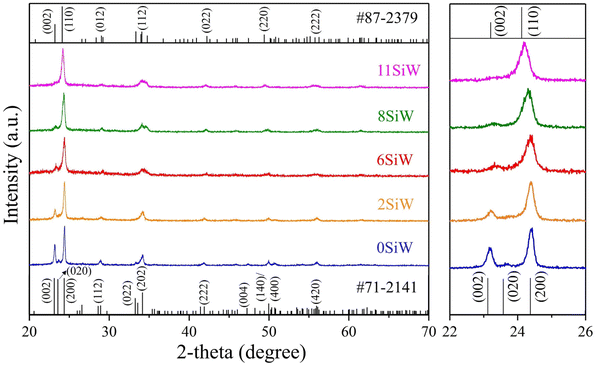
Table 2 shows the Si doping concentrations in the prepared WO3 films, which were determined by EDS analysis. As expected, the Si content in the films increased as the sputter power at the Si target increased, which was about 2.3 at%, 6.3 a%, 7.7 at% and 10.9 at% for powers of 20 W, 30 W, 40 W, and 50 W, respectively. For convenience, the samples are named according to their Si concentration in the following discussions, i.e., 0SiW, 2SiW, 6SiW, 8SiW, and 11SiW (see Table 2). Fig. 1 shows the surface and cross-sectional SEM micrographs, which appear to have similar morphologies for films of different Si doping levels, i.e., all the films were composed of fine particles with a smooth surface and a tidy interface between the film and the substrate. However, XRD revealed that the crystal structure of the films was constantly distorted as the Si content in the films increased, as shown in Fig. 2. The d-spacings of the undoped film (0SiW) matched well with the monoclinic phase of WO3 (PDF #71-2141), which has space group P21/n (no. 14). However, the reference pattern given in the database indicates that the (002), (020) and (200) peaks have similar intensity (i.e., 99.9%, 97.0%, 100%), whereas the pattern of 0SiW in Fig. 2 shows a greatly reduced intensity for (002) and (020); in particular, the (020) peak nearly disappears. Such changes in relative intensity show that the crystallites in the film did not orient randomly. Instead, they were grown preferentially along the (200) direction. It is noted that, although no peak from any secondary phase was observed, a small amount of amorphous SiO2 might be segregated in the samples with high Si doping level, which was not detectable by XRD.
Table 2 EDS result of films sputtered at different Si target powers
| Power (W) |
Si (at%) |
W (at%) |
Sample id |
| 0 |
0 |
100 |
0SiW |
| 20 |
2.26 |
97.74 |
2SiW |
| 30 |
6.25 |
93.75 |
6SiW |
| 40 |
7.66 |
92.34 |
8SiW |
| 50 |
10.90 |
89.10 |
11SiW |
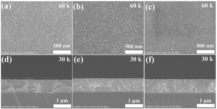 |
| | Fig. 1 Surface SEM images for (a) 0SiW, (b) 6SiW and (c) 11SiW. Cross-sectional SEM images for (d) 0SiW, (e) 6SiW and (f) 11SiW. | |
 |
| | Fig. 2 XRD patterns for the films of 0SiW, 2SiW, 6SiW, 8SiW and 11SiW. | |
As highlighted in the right-hand panel of Fig. 2, the Si doping results in the (200) peak shift constantly to the smaller 2θ side as the Si doping level increases. In contrast, the (002) peak shifts constantly to the larger 2θ side and its intensity decreases as the Si content in the films increases. In fact, it is found that the crystal structure of the Si-doped films with high concentration (≥6 at%) matches better with another monoclinic phase in the XRD powder diffraction database (PDF #87-2379), which has the space group Pc (no. 7). In addition to variations in peak position, Si doping also resulted in broadening of the XRD peaks (see right-hand panel of Fig. 2), as a consequence of reduced crystallite size (L) in the Si-doped films. Such peak broadening can be used to estimate the crystallite size by the well-known Scherrer equation, L = 0.89λ/β![[thin space (1/6-em)]](https://www.rsc.org/images/entities/char_2009.gif) cosθ, where λ is the X-ray wavelength and β is the full width at half maximum of the XRD peak at the diffraction angle 2θ. The calculated crystallite sizes were 47 nm, 34 nm, 29 nm, 29 nm and 28 nm for the films of 0SiW, 2SiW, 6SiW, 8SiW and 11SiW, respectively.
cosθ, where λ is the X-ray wavelength and β is the full width at half maximum of the XRD peak at the diffraction angle 2θ. The calculated crystallite sizes were 47 nm, 34 nm, 29 nm, 29 nm and 28 nm for the films of 0SiW, 2SiW, 6SiW, 8SiW and 11SiW, respectively.
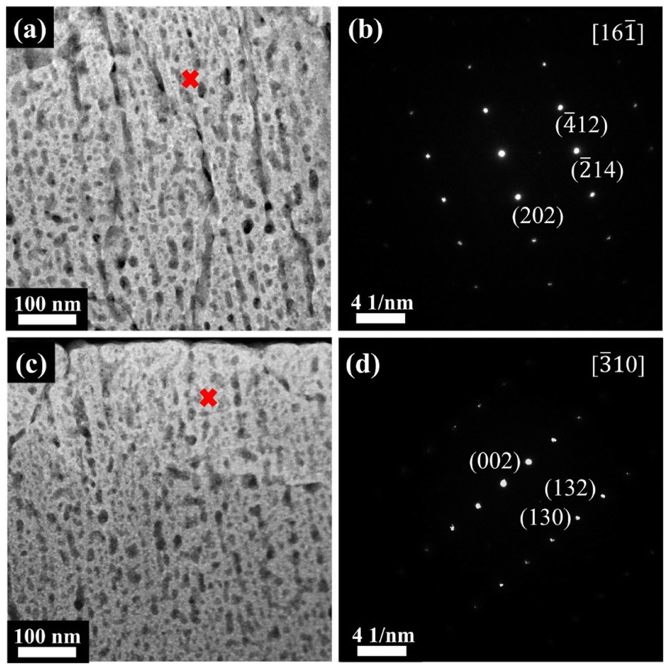
Although the SEM images in Fig. 1 show that the films are fairly dense, high-resolution TEM revealed that the films actually contained a high density of very small pores with diameters in the order of about 20 nm, as shown in Fig. 3(a) and (c) for the films of 0SiW and 6SiW, respectively. Apparently, such highly porous films are ideal for gas sensing applications because of the easy diffusion of gas molecules. Similar to what was observed in SEM, the TEM images in Fig. 3(a) and (c) show that Si doping does not result in a notable change in the nanomorphology of the WO3 films. On the other hand, nano-beam electron diffraction (NBED) revealed that, despite high porosity, the tiny crystallites in the films had high crystallinity, as manifested by the occurrence of well-defined diffraction patterns, as shown in Fig. 3(b) and (d). The diffraction pattern for 0SiW (Fig. 3(b)) can be indexed according to the P21/n monoclinic phase (PDF #71-2141), whereas the pattern for 6SiW (Fig. 3(d)) matches better with the Pc monoclinic phase (PDF #87-2379), which is consistent with the XRD result discussed above.
 |
| | Fig. 3 High-angle annular dark-field (HAADF) images: (a) 0SiW and (c) 6SiW. NBED patterns: (b) 0SiW and (d) 6SiW, which are indexed according to the P21/n phase (PDF #71-2141) and Pc phase (PDF #87-2379), respectively. Note: the red crosses in (a) and (c) are the locations where NBED was performed. | |
3.2 Gas sensing measurement
Fig. 4(a) shows a typical response curve, i.e., sensitivity (S) vs. time (t), recorded when pure air and test gas (5 ppm isoprene) were alternately injected into the chamber. The curve in Fig. 4(a) was measured at a working temperature of 350 °C with 6SiW film. It was found that either higher or lower Si doping in the WO3 film led to lower sensitivity, as illustrated in Fig. 4(b). The films exhibited a very short response time, between 0.3 and 1.5 s for films of different Si concentrations, as shown in Fig. 4(c). The recovery time was slightly longer than the response time, which varied between 1.2 and 3.0 s for films containing different amounts of Si (see Fig. 4(c)).
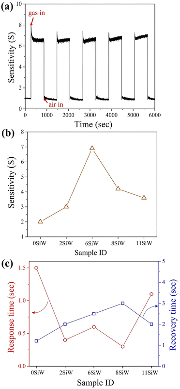 |
| | Fig. 4 (a) A typical curve of sensitivity vs. time, which was measured with 6SiW in 5 ppm isoprene at 350 °C. (b) Sensitivities measured with films of different Si doping level. (c) Response and recovery times of the films measured in 5 ppm isoprene at 350 °C. | |
To find the gas selectivity for isoprene, the sensitivities of several other common gases, such as methanol, ethanol, acetone, CO and CO2, were also measured for comparison. The results, which were recorded with films doped with different amounts of Si, are summarized in Fig. 5(a). They indicate that, except for the undoped film (i.e., 0SiW), all the films with Si doping have higher sensitivity for isoprene than for any of the reference gases. So, Si doping in WO3 has a notable effect on improving isoprene selectivity. In particular, the 6SiW film, which was shown earlier to have the highest isoprene sensitivity, also exhibits the best gas selectivity for isoprene. As indicated in Fig. 5(b), when measured with 6SiW film, the gas selectivity, which is defined as the sensitivity ratio between isoprene and a specific reference gas, ranges from 1.6 (for methanol/ethanol) to 4.6 (for CO), which are higher than the gas selectivities measured with all other films of different Si content. Fig. 5(c) compares the response and recovery times measured with isoprene and reference gases, which indicate that all of them have very short response times of about 1 s or less. However, there is a large variation in recovery time (2–110 s), and the quickest recovery times are observed with isoprene and acetone, which are 2.5 s and 2.3 s, respectively.
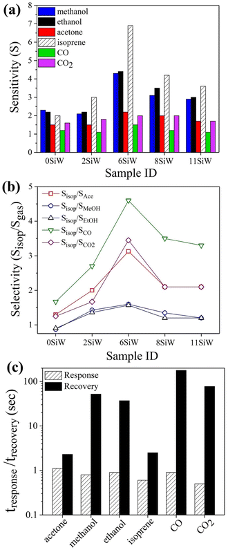 |
| | Fig. 5 (a) Comparison of gas sensitivities measured at 350 °C for isoprene, methanol, ethanol, acetone, CO and CO2 with films containing different amounts of Si. (b) Isoprene selectivity over other gases. (c) Response and recovery times of the above gases measured with 6SiW at 350 °C. | |
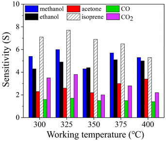
To identify the optimal working temperature, the gas sensing properties were measured with the sample (6SiW) being heated at different temperatures. Fig. 6 shows that the highest sensitivities are obtained at 325 °C for all the gases, e.g., the isoprene sensitivity measured at 325 °C is 7.7, compared to 7.1 measured at 300 °C and 6.9 at 350 °C. However, despite higher sensitivity at 325 °C, the gas selectivity of isoprene over the other gases is not better than that measured at 350 °C. In particular, the isoprene selectivity over methanol at 325 °C is nearly 20% less than that measured at 350 °C. There are many factors that may affect the temperature dependence of sensitivity, such as chemical reaction kinetics and gas absorption mechanisms (e.g., physisorption or chemisorption).34 So, different gases many have a different optimal working temperature determined by the combined effect of these factors. As a result, the highest sensitivity may not have to come with the best selectivity. Apparently, the latter is more important in terms of gas sensing applications.
 |
| | Fig. 6 Sensitivity vs. working temperature measured with 6SiW for various gases. | |
3.3 Electronic conduction and gas sensing mechanism
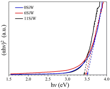
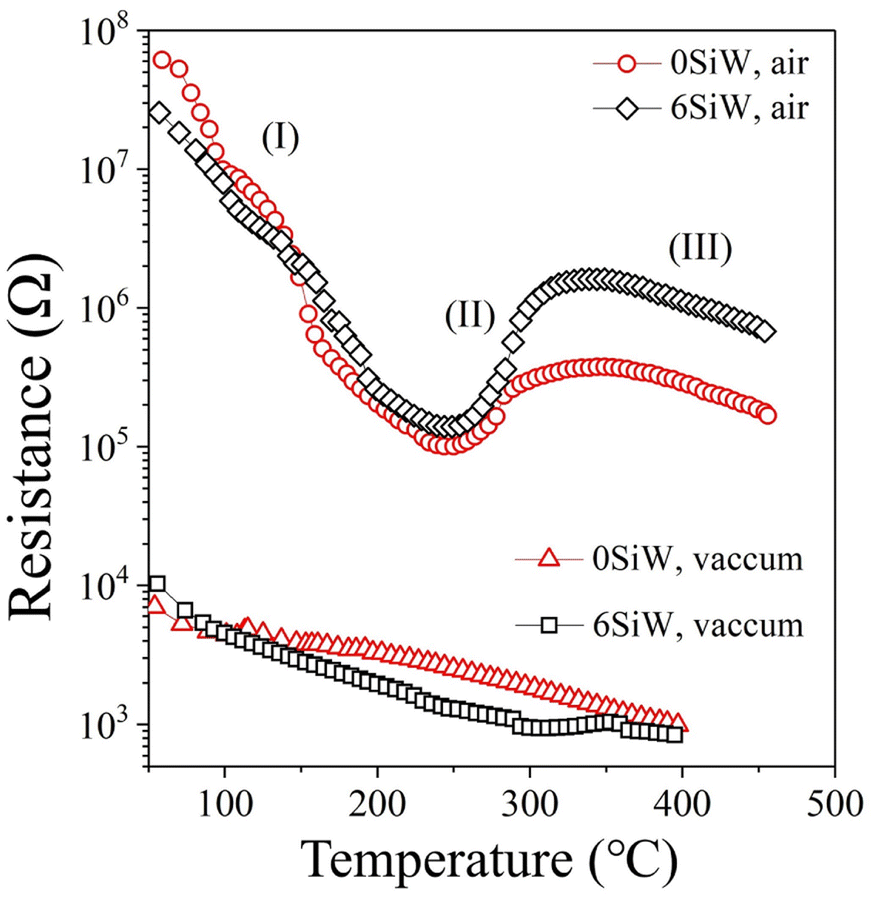
Fig. 7 shows the result of band gap measurements for the films. The undoped film (0SiW) has a band gap of 3.50 eV, which is approximately equal to the values previously reported for WO3 films grown in a similar way (i.e., sputter deposition plus post-annealing).35 The large band gap also agrees with the appearance of the films, which are highly transparent. Si doping results in a slight decrease in band gap, which is 3.45 eV and 3.40 eV for the films of 6SiW and 11SiW, respectively. Despite the large band gap, the films have finite conductivity, as shown in Fig. 8, which is known to result from the oxygen vacancies in films.36–38 Thermal activation to the conduction band of the electrons trapped in oxygen vacancies leads to an n-type conductivity of the oxygen-deficient WO3−x films.37,38 The presence of oxygen vacancies in our films was indeed confirmed by XPS, as shown in Fig. 9, where the asymmetric O 1s peak can be deconvoluted into three peaks at 530.3 eV, 531.5 eV and 533.0 eV, corresponding to the contributions from the lattice oxygen (OL), the oxygen in the vicinity of an oxygen vacancy (OV), and the adsorbed oxygen in the film (Oads), respectively.39,40 Also, the n-type conductivity of our films was confirmed by measurement of Mott–Schottky plots (see ESI†).
 |
| | Fig. 7 Tauc plots for 0SiW, 6SiW and 11SiW, showing the band gap which decreases as the Si doping increases. | |
 |
| | Fig. 8 R–T curves measured in vacuum (<7.5 mTorr) and in ambient air for the films of 0SiW and 6SiW. | |
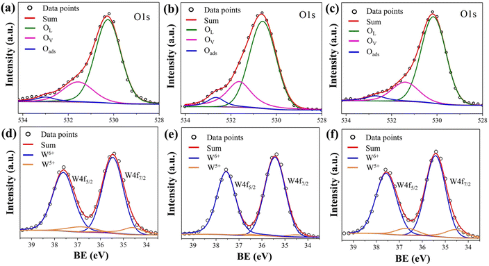 |
| | Fig. 9 XPS O 1s binding energy (BE) for (a) 0SiW, (b) 6SiW and (c) 11SiW. The percentage of each oxygen species, which is calculated according to the area under each peak, is listed in Table 3. XPS W4f peaks for (d) 0SiW, (e) 6SiW and (f) 11SiW. The calculated W5+/W6+ ratios are given in Table 3. | |
As defined earlier, gas sensitivity is the ratio of film resistance measured when pure air and test gas are injected, respectively, into the measurement chamber. One widely accepted mechanism accounting for such a change in resistance is based on the oxygen adsorption/desorption by the films.5,6 The SMO films for gas sensing are usually polycrystalline materials consisting of small crystallites, which are also termed grains in much of the literature. When such a film is exposed in air, oxygen molecules are absorbed at grain boundaries, which will extract electrons from the conduction band to form oxygen molecule ions (O2−) or oxygen ions (O−) dependent on temperature. This process causes band bending and an electron-depleted layer under the grain surface, leading to an increase in resistance. If the film is subsequently placed in a reduction gas (e.g., isoprene), the oxygen ions will react with the gas with the release of free electrons. As a consequence, the thickness of the depleted layer is reduced, leading to a decrease in resistance. Such a mechanism for resistance changes for an n-type SMO in a reduction gas may be described by eqn (1)–(5) below:5,6,17,41
| | |
O2(ads) + e− → O2(ads)− (<150 °C)
| (2) |
| | |
O2(ads)− + e− → 2O(ads)− (>150 °C)
| (3) |
| | |
C5H8(g) + 7O2(ads)− → 4H2O(g) + 5CO2(g) + 7e−
| (4) |
| | |
C5H8(g) + 14O(ads)− → 4H2O(g) + 5CO2(g) + 14e−
| (5) |
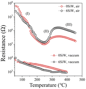
To confirm that such a mechanism indeed works with our films, the temperature-dependent resistance (R–T) of the films was measured under different atmospheres. As shown in Fig. 8, when measured in a vacuum (<7.5 mTorr), the film resistance decreases continuously as the temperature increases from 50 °C to 400 °C, which is typical behaviour for an n-type semiconductor due to thermal activation of electrons to the conduction band. However, when measured in air at ambient pressure, a very different R–T curve is observed. Firstly, the measured resistance is much larger due to band bending and the depleted layer at grain boundaries, which are brought about by the adsorbed oxygen, as explained above. Secondly, there is an upward turning point at about 250 °C and a downward turning point at about 330 °C, which are not observed in the R–T curves measured in a vacuum and therefore cannot be attributed to the transition from extrinsic to intrinsic conduction of a semiconductor. So, the upward/downward turning in the R–T curves measured in air is more likely to be related to the oxygen adsorption. In fact, such a curve shape is reminiscent of the plot of adsorbate density vs. temperature, where the upward and downward turning regions in the curve are correlated with the transition from equilibrium physisorption to irreversible chemisorption.42,43 So, the observed R–T behaviour in air may be understood as follows. The decrease in resistance from 50 °C to 250 °C (Section I of the R–T curve) is due to the deduction in physiosorbed oxygens as the temperature increases, which results in a narrower depleted layer and hence a decrease in resistance. The increase in resistance from 250 °C to 330 °C (Section II) is due to increased oxygen adsorption via the chemisorption process, which only becomes prominent at high temperature. The gradual drop in resistance at a temperature higher than 330 °C (Section III) is attributed to desorption of the chemisorbed oxygen.
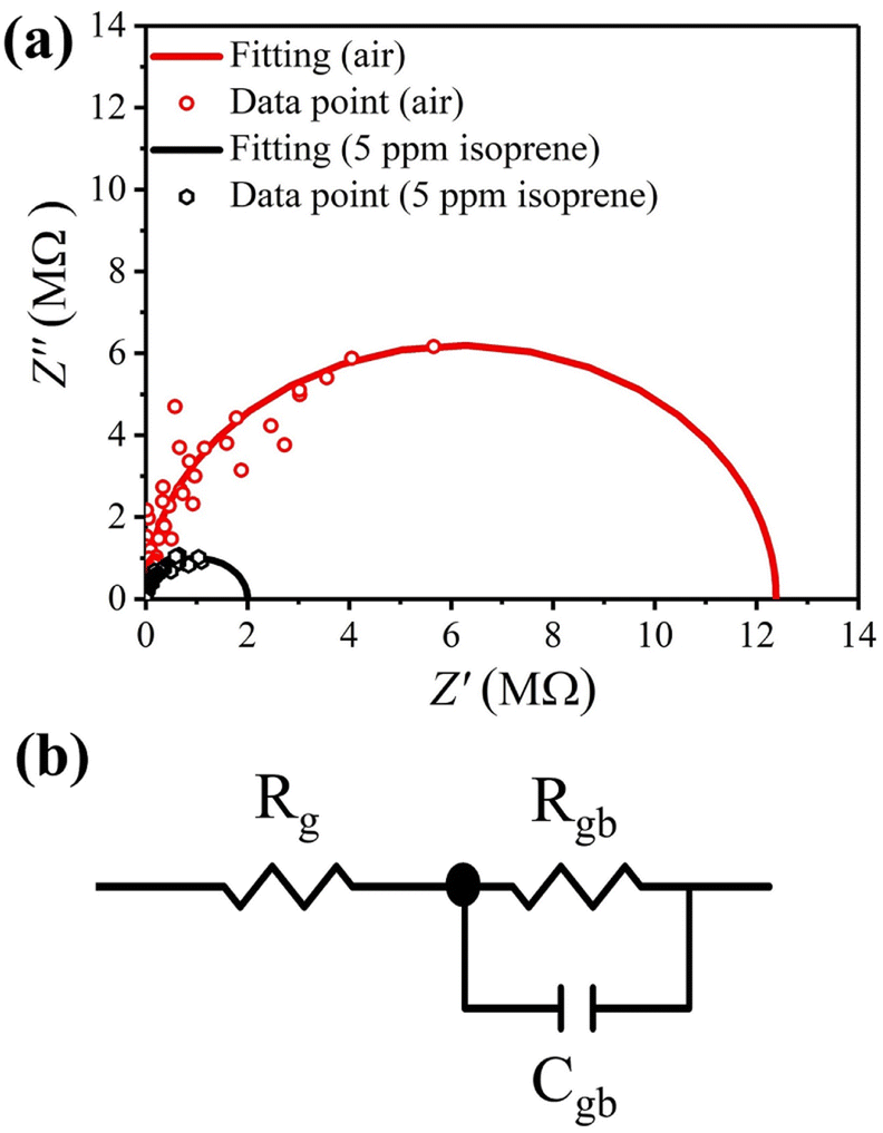
The above results indicate that band bending and the depleted layer at grain surface play a dominant role in the gas sensing mechanism. So, AC impedance analyses were carried out to discriminate the grain and grain-boundary contributions to the impedance changes under different ambient gases, which may be modelled by the equivalent circuit illustrated in Fig. 10(b). The grain boundaries are represented by a parallel subcircuit consisting of a capacitor (Cgb) and a resistor (Rgb), which is connected in series to another resistor (Rg) representing the grains.44 It is noted that the capacitance for grains is small, so its contribution to the impedance may be neglected in the measured frequency range (102 to 107 Hz) and therefore does not appear in the equivalent circuit. Shown in Fig. 10(a) are the Nyquist plots of the impedances measured at 350 °C in pure air and in 5 ppm isoprene, which were fitted with the equivalent circuit (Fig. 10(b)) using the software ZView® (II),45 to find the values of Cgb, Rgb, and Rg. The results are given in Table 4, which shows that grain resistance measured in air and isoprene changes only slightly from 320 Ω to 300 Ω, respectively, but there is a great decrease in the grain-boundary resistance, varying from 12.4 MΩ measured in air to 2.01 MΩ measured in isoprene.
 |
| | Fig. 10 (a) Nyquist plots of the impedances measured with the 6SiW film at 350 °C in pure air and in 5 ppm isoprene, which were fitted with the equivalent circuit in (b). | |
Table 3 The percentages of different oxygen species and W5+/W6+ ratio
| Sample id |
OL |
OV |
Oads |
W5+/W6+ |
| 0SiW |
74.0% |
21.7% |
4.3% |
12.3% |
| 6SiW |
67.9% |
25.7% |
6.4% |
2.7% |
| 11SiW |
75.2% |
19.5% |
5.2% |
11.8% |
Table 4 Impedances fitted with equivalent circuit
| |
In air |
In isoprene |
| Rg (Ω) |
320 |
300 |
| Rgb (Ω) |
1.24 × 10⁷ |
2.01 × 10⁶ |
| Cgb (F) |
1.74 × 10⁻¹⁰ |
5.28 × 10⁻¹¹ |
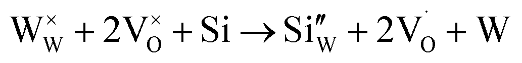
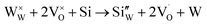
The improvement in isoprene sensitivity of WO3 films by Si doping (see Fig. 4(b)) may then be understood according to the above mechanism. As shown in Fig. 8, the chemisorption-induced resistance increase at temperatures higher than 300 °C is much more significant for 6SiW than for 0SiW, indicating that the former has higher gas adsorbability. This is consistent with the XPS result shown in Table 3, which indicates that the 6SiW film has higher adsorbed oxygen than 0SiW. The increase in gas adsorbability may result from both structural distortions, as discussed in Section 3.1, and the changes in defect structures that may be induced by the aliovalent doping of Si4+ at the W6+ site in WO3. Such doping leads to a reduction in cation valence, which may be compensated either by the increase in valence of the cations in a reduced state, i.e., W5+ ions that are presented in the undoped film (see Fig. 9(d)), or by the inclusion of charged anion vacancies, i.e., charged oxygen vacancies ( or
or  ). The defect equations for such charge compensation mechanisms may be written as follows:
| |
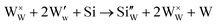 | (6) |
| |
 | (7) |
| |
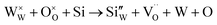 | (8) |
It is noted that  is the normal occupation of W6+ at the W site in WO3, whereas
  is W5+ at the W site, which has a negative charge. Eqn (7) and (8) lead to an increase in oxygen vacancies, whereas eqn (6) causes a decreased W5+/W6+ ratio. Both proposed compensation mechanisms seem to work for the 6SiW film. As shown in Table 3, the proportion of oxygen vacancies in 6SiW is increased, while the W5+/W6+ ratio is decreased.
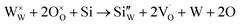
However, in the case of a very high doping level, i.e., 11SiW, the induced structural distortion may be too large to accommodate more defects, so that the oxygen vacancies are not increased, as indicated in Table 3. In contrast, the oxygen vacancies are decreased slightly and yet, although the W5+/W6+ ratio is also decreased, the amount of the deduction is much less. So, the charge compensation mechanism for 11SiW must be different. A likely one is that some of the oxygen vacancies in the undoped film are unionized oxygen vacancies (i.e.,  , each with two trapped electrons), which become charged upon Si doping, i.e.:
| |
 | (9) |
| |
 | (10) |
So, although 0SiW has more oxygen vacancies in total, 11SiW may have more charged oxygen vacancies. As indicated in Table 3, the adsorbed oxygen in 11SiW is lower than that in 6SiW, but higher than that in 0SiW. Similarly, as shown in Fig. 4(b), despite a lower sensitivity than 6SiW, the sensitivity of 11SiW is higher than that in 0SiW. Therefore, it appears that only the positively charged oxygen vacancies have the effect of increased gas adsorption, leading to higher sensitivity.
4. Conclusions
Pristine and Si-doped WO3 films were sputtered at RT from metallic targets and then annealed in air at 500 °C to form the oxide phase. The undoped film had a monoclinic structure with space group P21/n (no. 14), which gradually distorted with the increasing concentration of Si doping to another monoclinic phase of space group Pc (no. 7). The films appeared dense in SEM micrographs. However, TEM revealed that the films contained a high density of tiny pores with diameters of about 20 nm, which are ideal for gas sensing applications because of the easy diffusion of gas. The isoprene sensitivity of the WO3 films was greatly improved with Si doping and the films containing 6.3 at% Si showed the highest sensitivity of 7.7 for 5 ppm isoprene in air at a working temperature of 325 °C. However, although the sensitivity was lowered to 6.9 at a working temperature of 350 °C, the films showed better gas selectivity for isoprene over a range of reference gases, including methanol, ethanol, acetone, CO and CO2. The response and recovery times of the films were very fast, less than 1.5 and 3.0 s, respectively. The measurements of temperature-dependent resistance in a vacuum and in ambient air indicated that Si doping led to a great increase in chemisorption of oxygen at a temperature higher than 300 °C. The increased oxygen adsorption in the Si-doped films was confirmed in XPS and was correlated to the positively-charged oxygen vacancies in the films, which were increased by the aliovalent substitution of Si4+ with W6+. The improvement in gas sensitivity for the Si-doped films was then explained by their better oxygen absorbability.
Author contributions
P.-K. L.: investigation, data curation, preparation of graphics. Y. Q.: investigation, data curation. X. Q.: conceptualization, methodology, supervision, writing-original draft. L. H.: conceptualization, reviewing.
Conflicts of interest
The authors declare that they have no known competing financial interests or personal relationships that could have appeared to influence the work reported in this paper.
Notes and references
- S. Das and M. Pal, J. Electrochem. Soc., 2020, 167, 037562 CrossRef CAS.
- M. Kaloumenou, E. Skotadis, N. Lagopati, E. Efstathopoulos and D. Tsoukalas, Sensors, 2022, 22, 1238 CrossRef CAS PubMed.
- N. Alkhouri, T. Singh, E. Alsabbagh, J. Guirguis, T. Chami, I. Hanouneh, D. Grove, R. Lopez and R. Dweik, Clin. Transl. Gastroenterol., 2015, 6, e112 CrossRef CAS PubMed.
- J. Dadamio, S. Van den Velde, W. Laleman, P. Van Hee, W. Coucke, F. Nevens and M. Quirynen, J. Chromatogr. B: Anal. Technol. Biomed. Life Sci., 2012, 905, 17–22 CrossRef CAS PubMed.
- A. Dey, Mater. Sci. Eng., B, 2018, 229, 206–217 CrossRef CAS.
- A. Gurlo and R. Riedel, Angew. Chem., Int. Ed., 2007, 46, 3826–3848 CrossRef CAS PubMed.
- I. Kushch, B. Arendacká, S. Stolc, P. Mochalski, W. Filipiak, K. Schwarz, L. Schwentner, A. Schmid, A. Dzien, M. Lechleitner, V. Witkovský, W. Miekisch, J. Schubert, K. Unterkofler and A. Amann, Clin. Chem. Lab. Med., 2008, 46, 1011–1018 CAS.
- J. Williams, C. Stönner, J. Wicker, N. Krauter, B. Derstroff, E. Bourtsoukidis, T. Klüpfel and S. Kramer, Sci. Rep., 2016, 6, 25464 CrossRef CAS PubMed.
- N. Alkhouri, F. Cikach, K. Eng, J. Moses, N. Patel, C. Yan, I. Hanouneh, D. Grove, R. Lopez and R. Dweik, Eur. J. Gastroenterol. Hepatol., 2014, 26, 82–87 CrossRef CAS PubMed.
- M. Lawrence T, P. Robin and S. Bernard, Eur. J. Heart Failure, 2001, 3, 423–427 CrossRef PubMed.
- P. Mochalski, J. King, M. Haas, K. Unterkofler, A. Amann and G. Mayer, BMC Nephrol., 2014, 15, 43 CrossRef PubMed.
- J. van den Broek, P. Mochalski, K. Königstein, W. C. Ting, K. Unterkofler, A. Schmidt-Trucksäss, C. A. Mayhew, A. T. Güntner and S. E. Pratsinis, Sens. Actuators, B, 2022, 357, 131444 CrossRef CAS.
- D. Xu, K. Ge, S. Qi, Y. Chen, J. Qiu, S. Wang, Y. Tian, S. Fang, C. Liu and Q. Liu, J. Mater. Sci., 2020, 55, 7645–7651 CrossRef CAS.
- B. Han, J. Wang, W. Yang, X. Chen, H. Wang, J. Chen, C. Zhang, J. Sun and X. Wei, Sens. Actuators, B, 2020, 309, 127788 CrossRef CAS.
- Q. Zheng, J. H. Lee, S.-J. Kim, H.-S. Lee and W. Lee, Sens. Actuators, B, 2021, 327, 128892 CrossRef CAS.
- B. Han, H. Wang, W. Yang, J. Wang and X. Wei, Ceram. Int., 2021, 47, 9477–9485 CrossRef CAS.
- N. Saito, H. Haneda, K. Watanabe, K. Shimanoe and I. Sakaguchi, Sens. Actuators, B, 2021, 326, 128999 CrossRef CAS.
- O. O. Abe, Z. Qiu, J. R. Jinschek and P.-I. Gouma, Sensors, 2021, 21, 1690 CrossRef CAS PubMed.
- X. Wu, H. Wang, J. Wang, D. Wang, L. Shi, X. Tian and J. Sun, Colloids Surf., A, 2022, 632, 127752 CrossRef CAS.
- H. Jung, H. Min, J. Hwang, J. Kim, Y.-S. Choe, H.-S. Lee and W. Lee, Appl. Surf. Sci., 2022, 586, 152827 CrossRef CAS.
- S.-W. Park, S.-Y. Jeong, Y. K. Moon, K. Kim, J.-W. Yoon and J.-H. Lee, ACS Appl. Mater. Interfaces, 2022, 14, 11587–11596 CrossRef CAS PubMed.
- W. Guo, L. Huang, X. Liu, J. Wang and J. Zhang, Sens. Actuators, B, 2022, 354, 131243 CrossRef CAS.
- X. Xing, L. Du, C. Wang, D. Feng, G. Liu and D. Yang, Sens. Actuators, B, 2022, 372, 132669 CrossRef CAS.
- C. Zhang, J. Wang, Z. Zhang, J. Gong and H. Wang, RSC Adv., 2023, 13, 15826–15832 RSC.
- S. J. Park, Y. K. Moon, S.-W. Park, S. M. Lee, T.-H. Kim, S. Y. Kim, J.-H. Lee and Y.-M. Jo, ACS Appl. Mater. Interfaces, 2023, 15, 7102–7111 CrossRef CAS PubMed.
- L. Chen, Q. Yu, C. Pan, Y. Song, H. Dong, X. Xie, Y. Li, J. Liu, D. Wang and X. Chen, Talanta, 2022, 246, 123527 CrossRef CAS PubMed.
- A. T. Guntner, N. J. Pineau, D. Chie, F. Krumeich and S. E. Pratsinis, J. Mater. Chem. B, 2016, 4, 5358–5366 RSC.
- W. Yu, Z. Shen, F. Peng, Y. Lu, M. Ge, X. Fu, Y. Sun, X. Chen and N. Dai, RSC Adv., 2019, 9, 7723–7728 RSC.
- S. Cao and H. Chen, J. Alloys Compd., 2017, 702, 644–648 CrossRef CAS.
- C. Dong, R. Zhao, L. Yao, Y. Ran, X. Zhang and Y. Wang, J. Alloys Compd., 2020, 820, 153194 CrossRef CAS.
- D. Bonardo, N. L. W. Septiani, F. Amri, Estananto, S. Humaidi, Suyatman and B. Yuliarto, J. Electrochem. Soc., 2021, 168, 107502 CrossRef CAS.
- I. C. Weber, H. P. Braun, F. Krumeich, A. T. Güntner and S. E. Pratsinis, Adv. Sci., 2020, 7, 2001503 CrossRef CAS PubMed.
- J. Broek, A. T. Güntner and S. E. Pratsinis, ACS Sens., 2018, 3, 677–683 CrossRef PubMed.
- C. Yuan, J. Ma, Y. Zou, G. Li, H. Xu, V. V. Sysoev, X. Cheng and Y. Deng, Adv. Sci., 2022, 9, 2203594 CrossRef CAS PubMed.
- I. Castro-Hurtado, T. Tavera, P. Yurrita, N. Pérez, A. Rodriguez, G. G. Mandayo and E. Castaño, Appl. Surf. Sci., 2013, 276, 229–235 CrossRef CAS.
- M. N. Wubeshet Sahle, J. Solid State Chem., 1983, 48, 154–160 CrossRef.
- M. Gillet, C. Lemire, E. Gillet and K. Aguir, Surf. Sci., 2003, 532–535, 519–525 CrossRef CAS.
- J. Molenda and A. Kubik, Phys. Status Solidi B, 1995, 191, 471–478 CrossRef CAS.
- Z. Wang, X. Mao, P. Chen, M. Xiao, S. A. Monny, S. Wang, M. Konarova, A. Du and L. Wang, Angew. Chem., Int. Ed., 2019, 58, 1030–1034 CrossRef CAS PubMed.
- A. P. Shpak, A. M. Korduban, M. M. Medvedskij and V. O. Kandyba, J. Electron Spectrosc. Relat. Phenom., 2007, 156–158, 172–175 CrossRef CAS.
- W. C. Chang, S. C. Lee and X. Qi, J. Electrochem. Soc., 2010, 157, 245–250 CrossRef.
- M. Batzill and U. Diebold, Prog. Surf. Sci., 2005, 79, 47–154 CrossRef CAS.
- S. R. Morrison, The Chemical Physics of Surfaces, Springer, New York, 2nd edn, 1990, ch. 7, pp. 251–296 Search PubMed.
- V. Balasubramani, S. Chandraleka, T. S. Rao, R. Sasikumar, M. R. Kuppusamy and T. M. Sridhar, J. Electrochem. Soc., 2020, 167, 037572 CrossRef CAS.
- K. R. Cooper, M. Smith and D. Johnson, Sensors, 2008, 8, 1774–1796 CrossRef PubMed.
|
| This journal is © The Royal Society of Chemistry 2024 |
Click here to see how this site uses Cookies. View our privacy policy here. 
 Open Access Article
 This Open Access Article is licensed under a Creative Commons Attribution-Non Commercial 3.0 Unported Licence
 *ab and
Liji Huangc
*ab and
Liji Huangc


 or
or  ). The defect equations for such charge compensation mechanisms may be written as follows:


 is the normal occupation of W6+ at the W site in WO3, whereas
  is W5+ at the W site, which has a negative charge. Eqn (7) and (8) lead to an increase in oxygen vacancies, whereas eqn (6) causes a decreased W5+/W6+ ratio. Both proposed compensation mechanisms seem to work for the 6SiW film. As shown in Table 3, the proportion of oxygen vacancies in 6SiW is increased, while the W5+/W6+ ratio is decreased.
 , each with two trapped electrons), which become charged upon Si doping, i.e.: