 Open Access Article
High conductivity characteristics of phosphorus-doped nanocrystalline silicon thin films by KrF pulsed excimer laser irradiation method
Xiang Wangab,
Chao Song *ac,
Boxu Xud and
Huan Yang
 c
c
aChaozhou Branch of Chemistry and Chemical Engineering Guangdong Laboratory, Chaozhou 521041, China
bDepartment of Physics and Electrical Engineering, Hanshan Normal University, Chaozhou 521041, China
cSchool of Materials Science and Engineering, Hanshan Normal University, Chaozhou 521041, China. E-mail: chaosong@hstc.edu.cn
dSchool of Science, University of Science and Technology Liaoning, Anshan 114051, China
First published on 2nd April 2024
Abstract
The microstructure and high conductivity properties of phosphorus-doped nanocrystalline silicon films were investigated on samples prepared by a plasma-enhanced chemical vapor deposition technique and the KrF pulsed excimer laser irradiation method. The results of Fourier transform infrared spectroscopy and Raman spectroscopy show that Si nanocrystallites with an average diameter of 2 nm to 3 nm are formed in the film. The degree of crystallinity increases with the increase of laser radiation intensity, while the content of hydrogen decreases gradually. More phosphorus atoms are substitutionally incorporated into the nc-Si dots under higher laser irradiation fluence, which is responsible for the high dark conductivity. By controlling the laser fluence at 1.0 J cm−2, the dark conductivity as high as 25.7 S cm−1 can be obtained. Based on the measurements of temperature-dependent conductivity, the carrier transport processes are discussed. The phosphorus doping and the increase of electron concentration are considered to be the reason for high dark conductivity and extremely low conductivity activation energy.
1. Introduction
Recently, numerous efforts have been devoted to exploring an efficient silicon-based light source owing to its potential application in monolithic optoelectronic integration.1–3 Among them, hydrogenated nanocrystalline silicon (nc-Si:H) is considered to be one of the most likely materials to be applied in silicon-based light sources in the future. In addition, some nanoelectronic devices are also fabricated using nc-Si:H due to its advantages, such as adjustable band gap width, high radiative recombination efficiency and good compatibility with silicon micro–nano processing technology.4–6 But, most of the research studies have been carried out based on unintentionally doped nc-Si:H materials.7,8 Only a few studies have been concerned with the impurity doping in nc-Si to develop high performance Si NCs-based devices.9,10 Due to the coexistence of nanocrystalline and amorphous phases, intrinsic nc-Si film has low dark conductivity and high conductivity activation energy, which is considered to be harmful to the device performance and stability. The degree of crystallinity and size of the intrinsic nc-Si films significantly affect its optical and electrical properties. By thermal annealing or laser crystallization technology, the degree of crystallinity can be improved, resulting in the elevated dark conductivity. Phosphorus (P) doping is another way to improve the conductivity of nc-Si thin films. Due to the influence of the quantum confinement effect, surface–interface effect and self-cleaning effect, the P doping characteristic in nc-Si is significantly distinct from that in bulk silicon.11–14 For example, in bulk silicon doping, phosphorus and boron impurities are incorporated into bulk silicon substitutionally. Due to the small ionization energy of phosphorus and boron, they can be ionized to provide carriers at room temperature, which significantly improves the electric conductivity. Whereas, the initial theoretical simulation and experimental studies both have indicated that doping in quantum confined materials is quite difficult due to the large energy of formation of n- and p-type impurities. The P atoms tend to locate near the surface for the H-passivated Si NCs. The research work on the key problems such as the impurity position distribution, doping efficiency and influence of impurities on electrical properties has not been fully investigated so far. Meanwhile, a few works reported the role of P doping in Si NCs on the electronic transport behavior.15,16Compared to thermal annealing, excimer pulsed laser irradiation is a low temperature process due to the short pulse length and optical absorption depth, which is very important for minimizing the damage to the glass substrates. In our previous work,17 intrinsic nc-Si films were prepared from hydrogenated amorphous silicon films by using a KrF pulsed excimer laser irradiation method. It was found that the dark conductivity changed from 10−9 S cm−1 to 5.9 × 10⁻³ S cm−1 with increasing the laser fluence from 0 J cm−2 to 1.0 J cm−2, while the corresponding conductivity activation energy decreases from 0.77 eV to 0.18 eV. In order to further investigate and improve the electrical properties of nanocrystalline silicon films, we fabricate P-doped hydrogenated amorphous silicon films in a radio frequency (rf) plasma-enhanced chemical vapor deposition (PECVD) system. The KrF pulsed excimer laser irradiation technique is utilized to crystallize the thin hydrogenated amorphous silicon film and successfully fabricate P-doped nc-Si films. The degree of crystallinity, optical gap and electrical properties of the P-doped films before and after laser irradiating are investigated at various laser fluence. It is found that P-doped Si nanostructure with high crystallinity can be obtained by using laser irradiation. The conductivity of P doped nc-Si thin films increased from 1.2 × 10⁻³ S cm−1 to 25.7 S cm−1 with increasing the laser fluence from 0 J cm−2 to 1.0 J cm−2. Compared to non-doped amorphous Si and nc-Si film, it is found that the electric conductivity can greatly increase by P doping and laser irradiation.
2. Materials and methods
P-doped hydrogenated amorphous silicon (a-Si:H) films were fabricated on quartz plates and double-polished c-Si substrates in radio frequency plasma-enhanced chemical vapor deposition (PECVD) system by using 1% phosphine (PH3) gas in hydrogen (H2) mixed with pure silane (SiH4). The gas flow rate of SiH4 and PH3 is 5 and 1 sccm (standard cubic centimeter per minute), respectively. During the growth process, the radio frequency power, chamber pressure and substrate temperature were kept at 30 W, 10 mTorr and 250 °C, respectively. After deposition the samples were irradiated by KrF pulsed excimer laser pulse duration of 30 ns and with a wavelength of 248 nm. Only a single shot was employed and the laser fluence was in the range of 0.5 to 1.0 J cm−2. The laser treatment was carried out in ambient air at normal incidence after padding through a rectangular quartz mask. The laser beam was focused and the final irradiation area on the film surface was about 0.5 × 1 cm2. The thickness of the as-deposited film is about 360 nm. After laser irradiation, it is found that the thickness of films is almost none changed, which implies that films should be not damaged by laser irradiation. As shown in the previous research work, the films will be ablated after laser irradiation, and the ablation threshold depends on pulse fluence, duration and film thickness. In this work, the low laser fluence and short laser pulse duration are used to crystallize the thin hydrogenated amorphous silicon film in order to minimize the damage by laser irradiation.Raman signals were detected by a Jobin Yvon Horiba HR800 spectrometer with the 488 nm line of an Ar+ laser as an excitation light source with the power of 15 mW. During Raman spectra registration, the micro-Raman setup was not used and the diameter of sport was about 100 micrometers. The optical absorption of the films was measured at room temperature by Shimadzu UV-3600 spectrophotometer. Bonding structures of samples were characterized by using Fourier-transform infrared (FT-IR) spectroscopy (Nexus 870). The TECNAI F20 FEI high resolution transmission electron microscopy (HRTEM) was employed to reveal the formation of nanocrystalline silicon and their sizes. A pair of co-planar aluminum electrodes was made with the vacuum thermal evaporation method. The temperature-dependent dark conductivity was measured using a Keithley 610C electrometer. Before the measurements, all the samples were heated at 150 °C for 30 min to remove the absorbance from the films and the measurement temperature is in a range of room temperature to 423 K.
3. Results
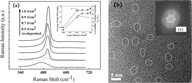
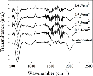
Fig. 1(a) shows the Raman spectra of the as-deposited sample and the samples after excimer laser irradiation at different laser fluence. As generally observed in the Raman spectra of nc-Si:H films, three peaks appear in the Raman spectra, a broad peak at about 480 cm−1, which is characteristic the transverse-optical (TO) vibration mode of amorphous silicon, a sharp peak at about 520 cm−1, which is characteristic of crystalline Si, and a peak at about 500 to 510 cm−1, which is related to the interfaces of Si nano-crystals with a-Si matrix. As shown in Fig. 1(a), the Raman spectra for the as-deposited film only displays the broad amorphous peak centered at 480 cm−1, which implies that the as-deposited samples are purely amorphous. As shown in the Gaussian deconvoluted Raman spectrum of sample irradiated with fluence of 0.5 J cm−2 in Fig. 1(a), the Raman spectra for the films after laser irradiation include not only the amorphous peak at 480 cm−1, but also crystalline related peaks at around 500 cm−1 to 510 cm−1, indicating that the film is composed of the amorphous phase and crystalline phase. With increasing the laser fluence, the crystalline related peak intensity and position increase and shift toward 520 cm−1, indicating the mean size of grains increases. In order to further study the microstructures of crystallized Si films, Gaussian deconvolution of the Raman spectra was performed for samples. The average grain size for the nc-Si is estimated according to the phonon confinement model.18 Meantime, the volume fraction of crystallized component (Xc) is deduced from the expression Xc = Ic/(Ic + 0.88IA), where Ic and IA denote the integrated intensities of the crystalline and amorphous peaks, respectively.18 The inset of Fig. 1(a) shows the average grain size and Xc in relation to the laser fluence evaluated from the Raman spectra shown in Fig. 1(a). It can be seen that the volume fraction of crystallized component increases from 48% to 70% as increasing the laser fluence from 0.5 J cm−2 to 1.0 J cm−2. Meanwhile, the size of crystallized Si also increases slightly as increasing the laser fluence, and the average grain size is in the range of 2–3 nm. In order to obtain direct evidence for the presence of Si nanocrystals, high resolution TEM was performed to study the microstructures of samples. As shown in Fig. 1(b), the cross-section HRTEM image of sample irradiated with fluence of 0.5 J cm−2 is given. It is found that the nanocrystals can be observed, and the average grain size is in the range of 2–3 nm, which is consistent with the size estimated from Raman spectra discussed above, indicating that the size of nanocrystalline grains is relatively uniform in films.19 The main orientation [111] of the nanocrystalline silicon can be obtained from the inset of Fig. 1(b), which is the fast Fourier transformation (FFT) of Fig. 1(b), revealing that the nanocrystalline silicon grains of the nc-Si:H thin film preferentially grow in [111] orientation. Therefore it can be concluded that nanocrystalline Si films with small grain size and high crystallinity can be formed by excimer laser irradiation.The FT-IR spectra were used to investigate the bonding configurations of samples. Fig. 2 shows the FT-IR spectra for samples before and after excimer laser irradiation. It is clearly seen that the absorption intensity of the silicon hydride varies with the laser fluence. The intense absorption band located at 640 cm−1 is connected to the wagging mode of the silicon hydride (Si–H). In addition to the 640 cm−1, the band at 2000 cm−1 is assigned to the stretching mode of H–Si–Si3. As shown in Fig. 2, it can be seen that the intensity of hydrogen-related absorption bands decreases with increasing the fluence of laser. Quantitatively, the density of bonded hydrogen atoms was calculated from the integrated absorption coefficient of the Si–H wagging mode located at 640 cm−1 according to the following equation.20,21
 | (1) |
Fig. 3 shows the relation of optical band gap as a function of laser fluence. The optical band gap was deduced from the absorption spectra by Tauc method.22 The inset in Fig. 3 gives Tauc plot of (αhν)1/2 versus photon energy (hν) for the sample irradiated by laser with a fluence of 0.9 J cm−2. The Tauc plot of other sample is similar, so it is not shown in the inset in Fig. 3. It can be found in Fig. 3 that the optical band gap decreases from 1.79 eV to 1.66 eV as increasing the laser fluence from 0 J cm−2 to 1.0 J cm−2. It is well known that the content of hydrogen and the crystallinity of nc-Si films could influence the optical band gap of nc-Si films. The existence of more hydrogen in nc-Si:H films leads to a higher optical gap than the bulk Si. And higher content of hydrogen in film result in higher optical band gap. Moreover, some research work report that the grain boundary existing in the nc-Si films would cause a higher optical band gap. As shown in Fig. 1 and 2, the content of hydrogen decrease with increasing the fluence of laser, while the crystallinity increases with the fluence. The competitiveness between hydrogen and crystallinity leads to the decrease of optical band gap, implying that the reduction of hydrogen plays a dominant role in the optical band gap.
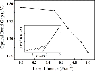 | ||
| Fig. 3 The values of optical band gap as a function of laser fluence. The inset gives the Tauc plots of the sample irradiated by laser with a fluence of 0.9 J cm−2. | ||
Fig. 4 shows the typical XPS spectra of Si 2p and P 2p peaks for the P-doped nanocrystalline Si films. As shown in Fig. 4(a), a strong peak at 99.3 eV is detected in the Si 2p spectrum, which can be assigned to the Si0 signal. A relatively weak signal at 102.6 eV can also be seen, which is related to the Si4+ originating from the oxidized Si.23 It implies that the oxygen atoms exist in the film mainly caused by irradiation process and exposure to air. Fig. 4(b) shows the P 2p spectrum of the P-doped nc-Si films. A signal at 128.4 eV associating with Si–P bond can be found in P 2p spectrum, which implies that P atoms have been doped into nc-si thin films and bonded to the Si atoms.
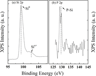 | ||
| Fig. 4 The typical XPS spectra of Si 2p and P 2p peaks for the P-doped nc-Si film irradiated by laser with a fluence of 0.5 J cm−2. | ||
Fig. 5 shows the dark conductivity of P doped nc-Si films and non-doped nc-Si films. It can be clearly seen that the dark conductivity of P doped nc-Si films is much higher than that of non-doped ones. The dark conductivity of as-deposited P doped and non-doped film is 1.2 × 10⁻³ S cm−1 and 5.1 × 10⁻⁹ S cm−1, respectively. The dark conductivity increases by six orders of magnitude by P doping, indicating that P atoms have been substitutionally incorporated into films. It can be proved by the XPS measurement results, as shown in Fig. 4(b). Because the ionization energy of the P atoms is low, some of the P atoms should ionize and provide a large number of electrons. The concentration of electrons in the film has been increased, leading to the increase of dark conductivity. It can be found that the dark conductivity of P doped nc-Si films greatly increase with increasing the laser fluence. After irradiating with fluence of 1.0 J cm−2, the dark conductivity reaches to 25.7 S cm−1, while the dark conductivity of as-deposited is 1.2 × 10⁻³ S cm−1. The dark conductivity increases by four orders of magnitude as the film transitions from amorphous phase to crystalline phase under the laser irradiation. It indicates that more P atoms are incorporated into the nc-Si dots and locate at the substitutional sites in the nc-Si with increasing the laser fluence, resulting in a large increase in the electron concentration. It was reported that P atoms would preferentially passivate the dangling bond defects at surface, and then be incorporated into the nc-Si. As the annealing temperature is increased, more P atoms are incorporated into the nc-Si. Other studies reported that the size of nc-Si dots affects the efficiency of the incorporation of phosphorus and/or boron atoms into silicon.24,25 The smaller size of nc-Si induces higher energy of formation, which makes it difficult for phosphorus atoms to be substitutionally incorporated into nc-Si. As shown in Fig. 1 and 2, the crystallinity and the average grain size of nc-Si film increase with the laser fluence accompany with the effusion of hydrogen. Under high energy density laser irradiation, the nc-Si is formed and part of P atoms diffuse to the surface of nc-Si to passivate the nc-Si dangling bond defects, generated by the effusion of hydrogen. Meantime, more P atoms are incorporated into the nc-Si dots due to the increase of grain size and more efficient diffusion of P atoms under higher laser irradiation fluence.26,27 Those incorporated P atoms are activated and provide more electrons to the conduction band. As a result, the dark conductivity as high as 25.7 S cm−1 is obtained in the P-doped nc-Si film formed by laser irradiation with a fluence of 1.0 J cm−2.
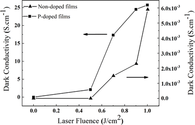 | ||
| Fig. 5 The dark conductivity of P doped nc-Si films and non-doped nc-Si films as a function of laser fluence. | ||
Fig. 6 shows the conductivity activation energy of the as-deposited sample and the samples after excimer laser irradiation at different laser fluence by temperature-dependent conductivity measurements. The temperature-dependent conductivity of samples shown in the inset of Fig. 6 is in good agreement with the Arrhenius plots, indicating that the carrier transport processes in samples are dominated by the thermally activated conduction mechanism.28 And the corresponding values of the conductivity activation energy obtained by using Arrhenius plots. It can be seen that the conductivity activation energy is 265 meV for the as-deposited P-doped films. After laser irradiation with fluence of 0.5 J cm−2, the conductivity activation energy rapidly decreases to 16.2 meV. As increasing the laser fluence from 0.5 J cm−2 to 1.0 J cm−2, the conductivity activation energy slowly decreases from 16.2 meV to 4 meV. Combining with dark conductivity measurement results shown in Fig. 5, it is thought that the increase of electron concentration caused by the substitutionally incorporated phosphorus atoms leads to the Fermi level shift toward conduction band, contributing to decrease of the activation energy. It is noticed that conductivity activation energy of samples irradiated by laser fluence from 0.7 J cm−2 to 1.0 J cm−2 is close to zero and remains nearly unchanged, indicating that the electron concentration is very high and the Fermi level pins at conduction band edge.29 As a result, the P-doped nc-Si films have high conductivity and the conductivity activation energy is approximate to zero. The mechanism of the electric transport should be primarily contributed by the conduction electrons introduced by phosphorus doping. It is concluded that nc-Si films with high conductivity and extremely low activation energy can be obtained by phosphorus doping combined with laser irradiation method.
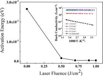 | ||
| Fig. 6 Conductivity activation energy as a function of laser fluence. The inset gives the temperature-dependent conductivity of samples. | ||
4. Conclusions
The P-doped nc-Si films were fabricated by plasma-enhanced chemical vapor deposition technique and the KrF pulsed excimer laser irradiation method. As increasing the laser fluence, the crystallinity of the films is increased accompany with the increase of grain size of nc-Si dots. Under higher laser irradiating, more P atoms are incorporated into the nc-Si substitutionally, led to the increase of electron concentration. As increasing the laser fluence, the electron concentration increases, induced the Fermi level shift to the conduction band edge. The P-doped nc-Si films with high dark conductivity (25.7 S cm−1) and extremely low activation energy (4 meV) can be obtained by using laser irradiation. The mechanism of the electric transport is contributed by the conduction electrons introduced by phosphorus incorporating.Author contributions
Xiang Wang: investigation, data curation, writing – original draft. Chao Song: conceptualization, writing – review & editing. Boxu Xu: formal analysis. Huan Yang: validation, software.Conflicts of interest
There are no conflicts to declare.Acknowledgements
This work was supported by the Self-innovation Research Funding Project of Hanjiang Laboratory (HJL202202A008) and University-Enterprise Collaborative Innovation Center for Big Health Industry (2022 Hybribio Special Project – 0002/b22088).References
- Y. Lei, D. R. Yang and D. S. Li, Enhanced optical and electronic properties of silicon nanosheets by phosphorus doping passivation, Materials, 2023, 16, 1079 CrossRef CAS PubMed.
- D. K. Li, J. M. Chen, T. Sun, Y. Y. Zhang, J. Xu, W. Li and K. J. Chen, Enhanced subband light emission from Si quantum dots/SiO2 multilayers via phosphorus and boron co-doping, Opt. Express, 2022, 30, 12308 CrossRef CAS PubMed.
- M. Zacharias and P. C. Kelires, Temperature dependence of the optical properties of silicon nanocrystals, Phys. Rev. B, 2020, 245122 CrossRef CAS.
- F. Romano, S. Angeloni, G. Morselli, R. Mazzaro, V. Morandi, J. R. Shell, X. Cao, B. W. Pogue and P. Ceroni, Water-soluble silicon nanocrystals as NIR luminescent probes for time-gated biomedical imaging, Nanoscale, 2020, 12, 7921–7926 RSC.
- E. M. T. Fadaly, A. Dijkstra, J. R. Suckert, D. Ziss, M. A. J. van Tilburg, C. Y. Mao, Y. Z. Ren, V. T. van Lange, K. Korzun, S. Kolling, M. A. Verheijen, D. Busse, C. Roedl, J. Furthmueller, F. Bechstedt, J. Stang, J. J. Finley, S. Botti, J. E. M. Haverkort and E. Bakkers, Direct-bandgap emission from hexagonal Ge and SiGe alloys, Nature, 2020, 205–209 CrossRef CAS PubMed.
- A. Sarkar, R. Bar, S. Singh, R. K. Chowdhury, S. Bhattacharya, A. K. Das and S. K. Ray, Size-tunable electroluminescence characteristics of quantum confined Si nanocrystals embedded in Si-rich oxide matrix, Appl. Phys. Lett., 2020, 116, 231105 CrossRef CAS.
- P. Lu, D. K. Li, Y. Q. Cao, J. Xu and K. J. Chen, Si nanocrystals-based multilayers for luminescent and photovoltaic device applications, J. Semicond., 2018, 39, 061007 CrossRef.
- Y. C. Zhang, C. Zhang, S. Li, X. Y. Dai, X. F. Ma, R. H. Gao, W. J. Zhou and M. Lu, Enhancing light emission of Si nanocrystals by means of high-pressure hydrogenation, Opt. Express, 2020, 28, 23320–23328 CrossRef CAS PubMed.
- P. Lu, W. W. Mu, J. Xu, X. W. Zhang, W. P. Zhang, W. Li, L. Xi and K. J. Chen, Phosphorus doping in Si nanocrystals/SiO2 multilayers and light emission with wavelength compatible for optical telecommunication, Sci. Rep., 2016, 6, 22888 CrossRef CAS PubMed.
- D. K. Li, Y. C. Jiang, P. Zhang, D. Shan, J. Xu, W. Li and K. J. Chen, The phosphorus and boron co-doping behaviors at nanoscale in Si nanocrystals/SiO2 multilayers, Appl. Phys. Lett., 2017, 110, 233105 CrossRef.
- A. R. Stegner, R. N. Pereira, K. Klein, H. Wiggers, M. S. Brandt and M. Stutzmann, Phosphorus doping of Si nanocrystals: Interface defects and charge compensation, Phys. B, 2007, 401–402, 541–545 CrossRef CAS.
- M. Perego, C. Bonafos and M. Fanciulli, Phosphorus doping of ultra-small silicon nanocrystals, Nanotechnology, 2010, 21, 025602 CrossRef PubMed.
- G. M. Dalpian and J. R. Chelikowsky, Self-purification in semiconductor nanocrystals, Phys. Rev. Lett., 2006, 96, 226802 CrossRef PubMed.
- D. J. Norris, A. L. Efros and S. C. Erwin, Doped nanocrystals, Science, 2008, 319, 1776–1779 CrossRef CAS PubMed.
- V. S. Waman, M. M. Kamble, S. S. Ghosh, A. Mayabadi and S. R. Jadkar, Highly conducting phosphorous doped n-type nc-Si:H films by HW-CVD for c-Si heterojunction solar cells, RSC Adv., 2012, 2, 9873–9880 RSC.
- X. Yu, W. Yu, X. Z. Wang, Y. Zheng, J. W. Zhang, Z. Y. Jiang and G. S. Fu, Effects of phosphorus doping on the optical and electronic properties of Si-quantum-dots/SiO2 multilayer films, Superlattices Microstruct., 2015, 78, 88–96 CrossRef CAS.
- C. Song, C. Li, J. Xu, R. Huang, X. Wang, J. Song and Y. Q. Guo, Improvement of the electrical properties of nanocrystalline silicon films by the KrF pulsed excimer laser irradiation method, Laser Phys., 2013, 23, 076002 CrossRef CAS.
- G. X. Cheng, K. J. Chen, W. Zhang, H. Xia and X. K. Zhang, Microstructural studies of non-crystalline solid silicon films by TO-like modes of Raman spectra, Phys. Status Solidi, 2010, 129, 421–434 CrossRef.
- P. Q. Luo, Z. B. Zhou, Y. J. Li, S. Q. Lin, X. M. Dou and R. Q. Cui, Effects of deposition pressure on the microstructural and optoelectrical properties of B-doped hydrogenated nanocrystalline silicon (nc-Si:H) thin films grown by hot-wire chemical vapor deposition, Microelectron. J., 2008, 39, 12–19 CrossRef CAS.
- P. Alpuim, V. Chu and J. P. Conde, Amorphous and microcrystalline silicon films grown at low temperatures by radio-frequency and hot-wire chemical vapor deposition, J. Appl. Phys., 1999, 86, 3812–3821 CrossRef CAS.
- T. Rajagopalan, X. Wang, B. Lahlouh, C. Ramkumar, P. Dutta and S. Gangopadhyay, Low temperature deposition of nanocrystalline silicon carbide films by plasma enhanced chemical vapor deposition and their structural and optical characterization, J. Appl. Phys., 2003, 94, 5252–5260 CrossRef CAS.
- A. Nakajima, Y. Sugita, K. Kawamura, H. Tomita and N. Yokoyama, Microstructure and optical absorption properties of Si nanocrystals fabricated with low-pressure chemical-vapor deposition, J. Appl. Phys., 1996, 80, 4006–4011 CrossRef CAS.
- M. Perego, C. Bonafos and M. Fanciulli, Phosphorus doping of ultra-small silicon nanocrystals, Nanotechnology, 2010, 21, 025602 CrossRef PubMed.
- W. He, Z. P. Li, C. Wen, H. Liu and W. Z. Shen, Size dependence of phosphorus doping in silicon nanocrystals, Nanotechnology, 2016, 27, 425710 CrossRef PubMed.
- Y. C. Jiang, D. K. Li, J. Xu, W. Li and K. J. Chen, Size-dependent phosphorus doping effect in nanocrystalline-Si-based multilayers, Appl. Surf. Sci., 2018, 461, 66–71 CrossRef CAS.
- J. M. Chen, D. K. Li, T. Sun, J. N. Han, Y. Y. Zhang, W. Li, J. Xu and K. J. Chen, Experimental observations on metal-like carrier transport and Mott hopping conduction behaviours in boron-doped Si nanocrystal multilayers, Nanotechnology, 2023, 34, 16LT01 CrossRef PubMed.
- J. N. Han, D. K. Li, T. Sun, J. M. Chen, Y. H. Wang, X. D. Pi, W. Li, L. Xu, J. Xu and K. J. Chen, First principles study on phosphorus or boron doping in si nanocrystals with various sizes embedded in SiO2 matrix, Phys. Scr., 2023, 98, 065007 CrossRef.
- S. Y. Myong, K. S. Lim and M. Konagai, Effect of hydrogen dilution on carrier transport in hydrogenated boron-doped nanocrystalline silicon-silicon carbide alloys, Appl. Phys. Lett., 2006, 88, 131 Search PubMed.
- D. Kar and D. Das, Opto-electronic properties of P-doped nc-Si-QD/a-SiC:H thin films as foundation layer for all-Si solar cells in superstrate configuration, J. Appl. Phys., 2016, 120, 025102 CrossRef.
| This journal is © The Royal Society of Chemistry 2024 |

