
 Open Access Article
 This Open Access Article is licensed under a Creative Commons Attribution-Non Commercial 3.0 Unported Licence
Surface modification of halide perovskite using EDTA-complexed SnO2 as electron transport layer in high performance solar cells†
Nuno Marques,
Santanu Jana,
Manuel J. Mendes ,
Hugo Águas,
Rodrigo Martins and
Shrabani Panigrahi*
,
Hugo Águas,
Rodrigo Martins and
Shrabani Panigrahi*
CENIMAT|i3N, Department of Materials Science, School of Science and Technology, NOVA University Lisbon and CEMOP/UNINOVA, Campus de Caparica, Caparica, 2829-516, Portugal. E-mail: s.panigrahi@campus.fct.unl.pt
First published on 17th April 2024
Abstract
The long-term performance of metal halide perovskite solar cells (PSCs) can be significantly improved by tuning the surface characteristics of the perovskite layers. Herein, low-temperature-processed ethylenediaminetetraacetic acid (EDTA)-complexed SnO2 (E-SnO2) is successfully employed as an electron transport layer (ETL) in PSCs, enhancing the efficiency and stability of the devices. The effects of EDTA treatment on SnO2 are investigated for different concentrations: comparing the solar cells' response with 15%–2.5% SnO2 and E-SnO2 based ETLs, and it was found that 7.5% E-SnO2 provided the best results. The improved surface properties of the perovskite layer on E-SnO2 are attributed to the presence of small amount of PbI2 which contributes to passivate the defects at the grain boundaries and films' surface. However, for the excess PbI2 based devices, photocurrent dropped, which could be attributed to the generation of shallow traps due to excess PbI2. The better alignment between the Fermi level of E-SnO2 and the conduction band of perovskite is another favorable aspect that enables increased open-circuit potential (VOC), from 0.82 V to 1.015 V, yielding a stabilized power conversion efficiency of 15.51%. This complex ETL strategy presented here demonstrates the enormous potential of E-SnO2 as selective contact to enhance the perovskite layer properties and thereby allow stable and high-efficiency PSCs.
Introduction
The emerging development of perovskite solar cells (PSCs) has been leading to exciting research in the field of photovoltaics in the past decade due to the PSCs' high solar-to-electric power conversion efficiency (PCE),1,2 low fabrication cost,3–5 band gap tunning capability,6 small exciton energy,7,8 excellent bipolar carrier transport, long charge diffusion length9 etc. Recent research efforts on new perovskite compositions, thin film growth, interfacial engineering and device architectures have resulted in remarkable PCEs ∼ 26% for single junction PSCs.10 The typical configuration of n-i-p structured PSCs usually consists of a glass substrate with a transparent conducting oxide (TCO) layer, followed by an n-type electron transport layer (ETL), a perovskite absorber layer, a p-type hole transport layer (HTL), and finally a metal contact.The ETL is a crucial component in PSCs, as it significantly influences the photovoltaic performance and charge dynamics of the device.11–13 For a device to work well, the ETL should meet some fundamental requirements: good optical transmittance to ensure that enough light is transmitted to the perovskite absorber, well matched energy level with perovskite materials to provide the desired open-circuit voltage (VOC), and a high electron mobility to efficiently remove carriers from the active layer to prevent charge recombination etc. Currently, nearly all PSCs with high PCE are based on mesoporous-type architecture,14,15 which frequently require high temperatures to sinter the mesoporous layer for optimal performance, compromising its low-cost advantage and limiting its application in flexible and tandem devices. On the other hand, planar-type PSCs consisting of stacked planar thin films have been developed using low-temperature and low-cost synthesis techniques. Compared to the more conventional TiO2, SnO2 is a more promising ETL candidate for highly efficient PSCs due to its higher transmittance, large bandgap (3.6–4.5 eV), superior optical and electric properties, band alignment with perovskite, and exceptional stability in the presence of moisture, heat, and light with negligible photoactivity.16 The lower conduction band and higher carrier mobility (240 cm2 (V−1 s−1)) of SnO2 leads to a more effective carrier transport.11,17
A number of methods, including spin-coating after solution processing, chemical bath deposition (CBD),18 atomic layer deposition (ALD),19 electrochemical deposition (ED)20 etc. have been utilized to produce low-temperature SnO2 films. For the first time in conventional planar-type PSCs, Ke et al.21 employed SnO2 thin film as an ETL and demonstrated a PCE of 16.02% with improved hysteresis. Afterwards, different types of SnO2 thin films have been investigated in PSCs, such as SnO2 nanostructured in different forms and SnO2 QDs.22–24 However, due to defects at the interfaces of perovskite and SnO2, a degradation on the PSCs' performance has been observed. This has been attributed to charge buildup at the ETL/perovskite interface, which is caused by the ETL's low electron mobility. On the other hand, self-doped defects on the surface of SnO2 (like Sn and O vacancies, surface hydroxyls, and others) have a big effect on the performance as well as on the stability of PSCs.25,26 In more detail, hydroxyl groups (–OH) and dangling bonds on the surface of SnO2 reduce the energy required to form oxygen vacancies and facilitate oxygen diffusion towards the perovskite lattice.27 Therefore, elemental doping,28–31 bilayer design,32,33 and interface modification11,34–36 on the SnO2 film were widely employed to enhance the performance of PSCs. Yang et al.37 employed an ETL composed of SnO2 complexed with ethylenediaminetetraacetic acid (EDTA) and showed that the Fermi level of EDTA-complexed SnO2 is better matched with the conduction band of the perovskite layer compared to conventional SnO2 ETL. It revealed the simultaneous advantages of hysteresis suppression and high VOC. These results represent a significant advancement in the development of high-performance PSCs and pave the way for further improvements in device efficiency and stability. Gong et al.38 reported the impact of the surface modification for SnO2 ETL on the stability and interfacial physicochemical characteristics of PSC devices. The addition of NH4F solution has the potential to modify the morphology of the SnO2 film, resulting in the filling of pinholes and cracks and the formation of a uniform and uninterrupted layer for the high performance PSCs.39 Keshtmand et al.40 reported the treatment of NH4Cl to modify the surface of SnO2 ETL to enhance the efficiency of planar PSCs, specifically in terms of open-circuit voltage (VOC). Muthukrishnan et al.41 applied oxygen plasma treatment to improve the quality of low-temperature processed SnO2 ETL to enhance the PSCs' efficiency. Cao et al.42 modified the surface defects of SnO2 ETL in PSCs by applying a fullerene derivative. As a result, the authors demonstrated an increase in electron transport and a reduction in charge recombination velocity, resulting in a highly efficient PSC with a PCE of 21.39%.
In this work, we adopt a simple and effective treatment by adding EDTA to commercially available SnO2 aqueous colloids. The objective is to modify the surface of SnO2 particles to enhance the stability of industrial SnO2 colloidal films, which serve as ETL in our PSCs. Here, EDTA treated SnO2 is denoted as E-SnO2. We have also conducted a comprehensive investigation by varying the concentration (15%–2.5%) of commercially available SnO2 and its EDTA-complexed counterpart (E-SnO2). Unlike previous studies, which often focused solely on one aspect of device optimization, our approach allowed us to simultaneously explore the properties of the resulting perovskite layers, and the performance of the corresponding best devices across a wide range of SnO2 and E-SnO2 concentrations. Due to its powerful chelation activity, EDTA offers good ETL modification in organic solar cells.43 The material characteristics of low-temperature treated E-SnO2 are comparable to those of high-temperature annealed SnO2. Therefore, E-SnO2 ETL-based PSCs exhibit a substantial enhancement in PCE, in comparison to the standard SnO2 ETL-based PSCs, due to enhancement in VOC and fill factor (FF). Moreover, E-SnO2 ETL aids to moderate the perovskite film by increasing the grain size and changing the surface potential, which can strongly reduce the charge recombination. Besides, E-SnO2 possesses high electron mobility, which facilitates the movement of electrons. However, the carrier extraction was possibly affected by the introduction of shallow traps for E-SnO2 ETL-based devices, upon excess presence of PbI2 in the perovskite film, resulting in a decrease of the short-circuit current. Overall, the investigation revealed that 7.5% E-SnO2 yielded the most favorable outcomes and the PCE for PSCs based on E-SnO2 ETL increased from 13.20% to 15.51%, relative to the control SnO2 based PSC. For prospective applications, this study demonstrates a promising route for the development of low-temperature fabricated PSCs with attractive cost-effectiveness.
Results and discussion
Fig. 1(a) and (b) show the schematic representation of the perovskite film formation on SnO2 and E-SnO2 ETLs, respectively. The ETLs were first deposited on glass/ITO substrate by spin-coating technique. After the annealing treatment, perovskite solution was then spun onto the ETL surface. Details of the experimental part are presented in the next section. Fig. 1(a) and (b) show the perovskite surface with large grains, however, the perovskite film on E-SnO2 show the similar morphology with PbI2 distributed into the GBs and on the surfaces of the perovskite film. To know the topological information of the perovskite films in greater depth, scanning electron microscopy (SEM) was conducted to compare the films morphology. To make SnO2 solutions with varying concentrations, the purchased SnO2 aqueous colloidal dispersion (15 wt%) was diluted with deionized water to achieve different concentrations of 10, 7.5, and 2.5 wt%. Simultaneously, E-SnO2 solutions were prepared by mixing EDTA solution with SnO2 colloidal solution in a proper ratio.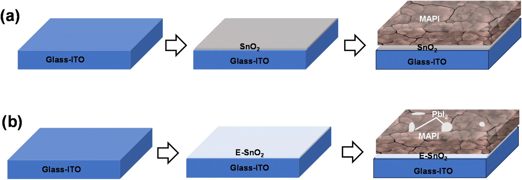 | ||
| Fig. 1 Schematic diagrams of perovskite film fabrication procedures: (a) on SnO2 ETL, (b) E-SnO2 ETL. | ||
The details of the preparation technique are described in the experimental section. Fig. 2(a) shows the surface morphology of the perovskite film on only SnO2 (15%) based ETL. Fig. 2(b)–(e) show the SEM images of the perovskite films on E-SnO2 (15%), E-SnO2 (10%), E-SnO2 (7.5%) and E-SnO2 (2.5%), respectively. It is observed that for the E-SnO2 based perovskite film, the pinholes in between the grains slowly decreased with decreasing the concentration of E-SnO2 and the appearance of PbI2 at the grain boundary and surfaces of the perovskite films. In the field of lead halide perovskite, SEM is typically optimized for the detection of secondary electrons, which convey only topological information. However, a portion of electrons that have been backscattered will also be detected, providing compositional information. The intensity of backscattered electrons is proportional to the average atomic number of the atoms in the sample, with regions with a higher average atomic number appearing brighter in typical images.44 As the average atomic number of PbI2 is higher than that of the MAPbI3 perovskite around it, therefore, bright PbI2 crystals can be seen on the surfaces of the perovskite films in Fig. 2(b)–(d), respectively. Because PbI2 (marked with white open circle) has a different contrast compared to perovskite grains.
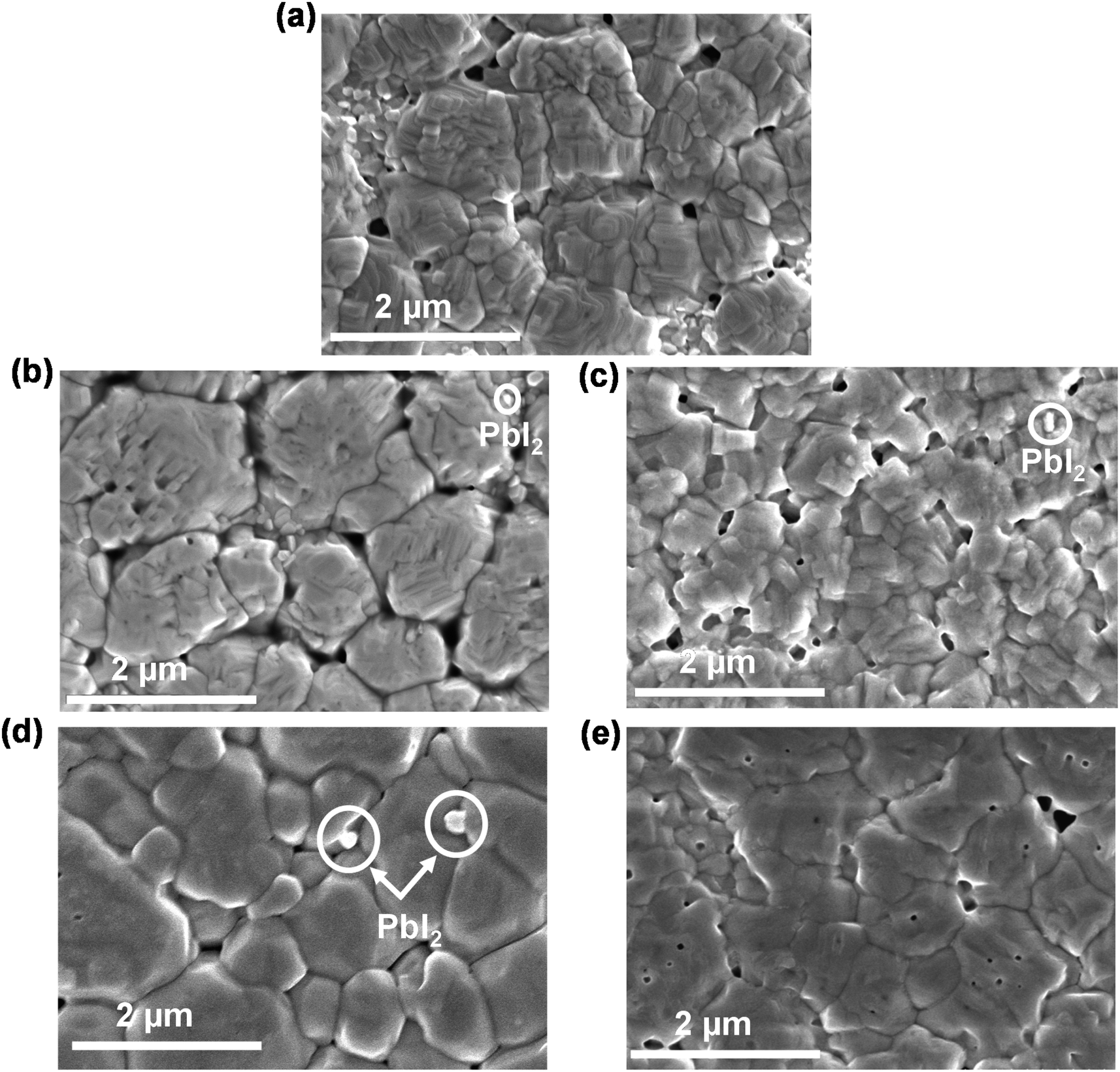 | ||
| Fig. 2 Surface morphology (FESEM image) of the perovskite films on (a) SnO2 (15%), (b) E-SnO2 (15%), (c) E-SnO2 (10%), (d) E-SnO2 (7.5%) and (e) E-SnO2 (2.5%) ETLs. | ||
Furthermore, X-ray diffraction (XRD) analysis is the most used method to detect the presence of crystalline PbI2 in a perovskite film. Fig. 3(a) shows the combined XRD pattern for perovskite films on SnO2 (15%), E-SnO2 (15%), E-SnO2 (10%), E-SnO2 (7.5%) and E-SnO2 (2.5%), respectively. In case of only SnO2 based perovskite film, the peaks correspond to the tetragonal phase of MAPbI3. However, the extra (001) diffraction peak for hexagonal PbI2 at 2θ = 12.6° is clearly observed for all E-SnO2 based perovskite films. The zoom view for the PbI2 peak clearly shows that the intensity is maximum for the 7.5% E-SnO2 based perovskite films. The intensity of the crystalline (001) PbI2 peak increases monotonically up to 7.5% and then starts to decrease when the concentration of E-SnO2 solution decreases after that. X-ray photoelectron spectroscopy (XPS) was used to examine the surface chemical composition of the perovskite films (MAPI) on different ETLs to determine the origin of the alterations in crystalline structure. Fig. 3(b) shows the full XPS spectra for only the perovskite films deposited on SnO2 (7.5%) and E-SnO2 (7.5%) ETLs, respectively. These spectra show the four main peaks centered at 138 eV, 286 eV, 402 eV and 619 eV, which were assigned to Pb 4f, C 1s, N 1s and I 3d, respectively. The high resolution XPS spectra for Pb 4f and I 3d peaks are shown in Fig. 3(c) and (d), respectively. For only SnO2 based MAPI film, the peaks of Pb 4f5/2 and Pb 4f7/2 were detected at 143.5 eV and 138.5 eV, respectively. For E-SnO2 based ETL, the Pb 4f peak pairs shifted to a slightly lower binding energy. A decrease in binding energy results from an increase in the electron screening effect as a result of an increase in electron density.45 This redshift in the binding energy can therefore be tentatively attributed to the interactions between uncoordinated PbI2 and the electron-rich N and O atoms, which increase the electron cloud density and decrease the electron affinity of PbI2 ions.46
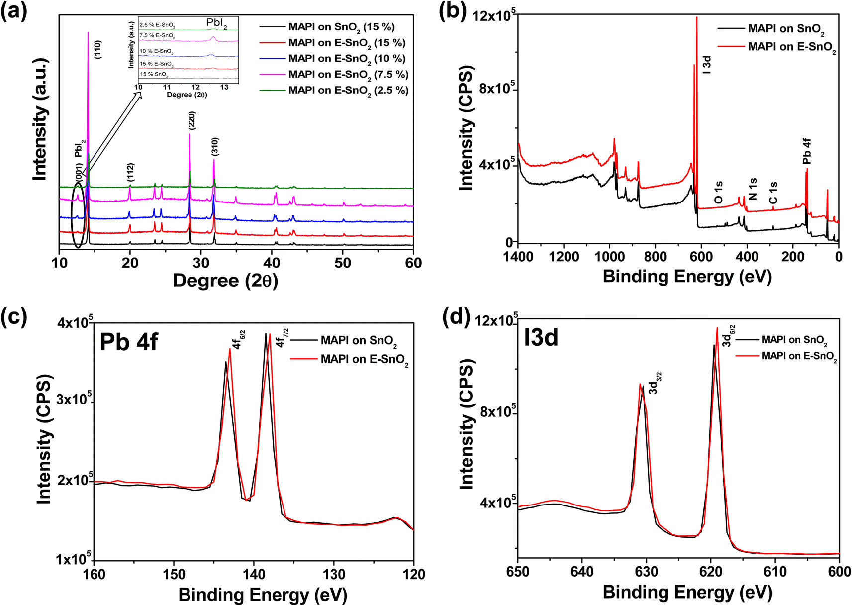 | ||
| Fig. 3 (a) X-ray diffraction (XRD) pattern of the perovskite films on different ETLs. Zoom view of the PbI2 peak only (Inset). (b) XPS survey spectra of the perovskite films deposited on SnO2 and E-SnO2 ETLs. XPS spectra for only (c) Pb 4f and (d) I 3d peaks. | ||
The UV-visible spectra provide information about the influence of EDTA on the optical properties of MAPI films. The UV-visible spectra for all samples show a typical MAPbI3 absorbance, with a peak at 747 nm. When compared to only SnO2 based MAPI film, E-SnO2 based MAPI films showed similar absorption with a slightly higher optical absorption intensity, as shown in Fig. 4(a). For the perovskite film on E-SnO2 (7.5%), the intensity is much higher than others. This result is attributable to the increased crystallinity of the perovskite film due to E-SnO2 ETL. Steady-state photoluminescence (PL) was also used to examine the recombination kinetics of the perovskite films formed on with and without EDTA based ETLs. Fig. 4(b) displays the respective PL spectra of the perovskite films on SnO2 and E-SnO2 based ETLs. All the films demonstrate a prominent emission peak at around 782 nm, which corresponds to the radiative recombination process from the valence band to the conduction band of perovskite under an excitation wavelength of 400 nm. Notably, a significantly decreased PL intensity is observed for the perovskite films deposited on E-SnO2 than that for SnO2 based perovskite films. The presence of PbI2 at the E-SnO2 based perovskite film surfaces and GBs might reduce the deep defects, thus resulting in reduced carrier recombination.47,48
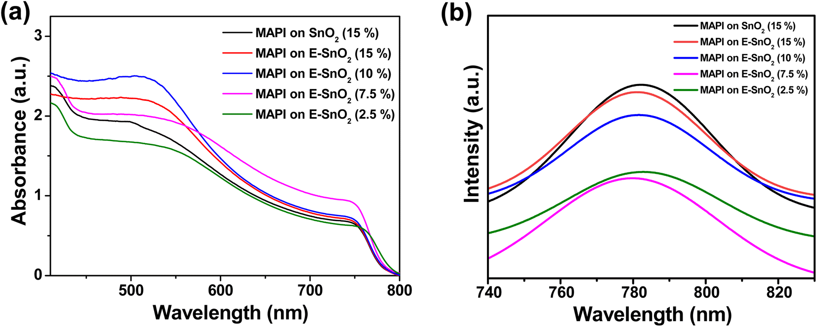 | ||
| Fig. 4 (a) Absorbance and (b) steady-state PL spectra of perovskite films with various ETLs. | ||
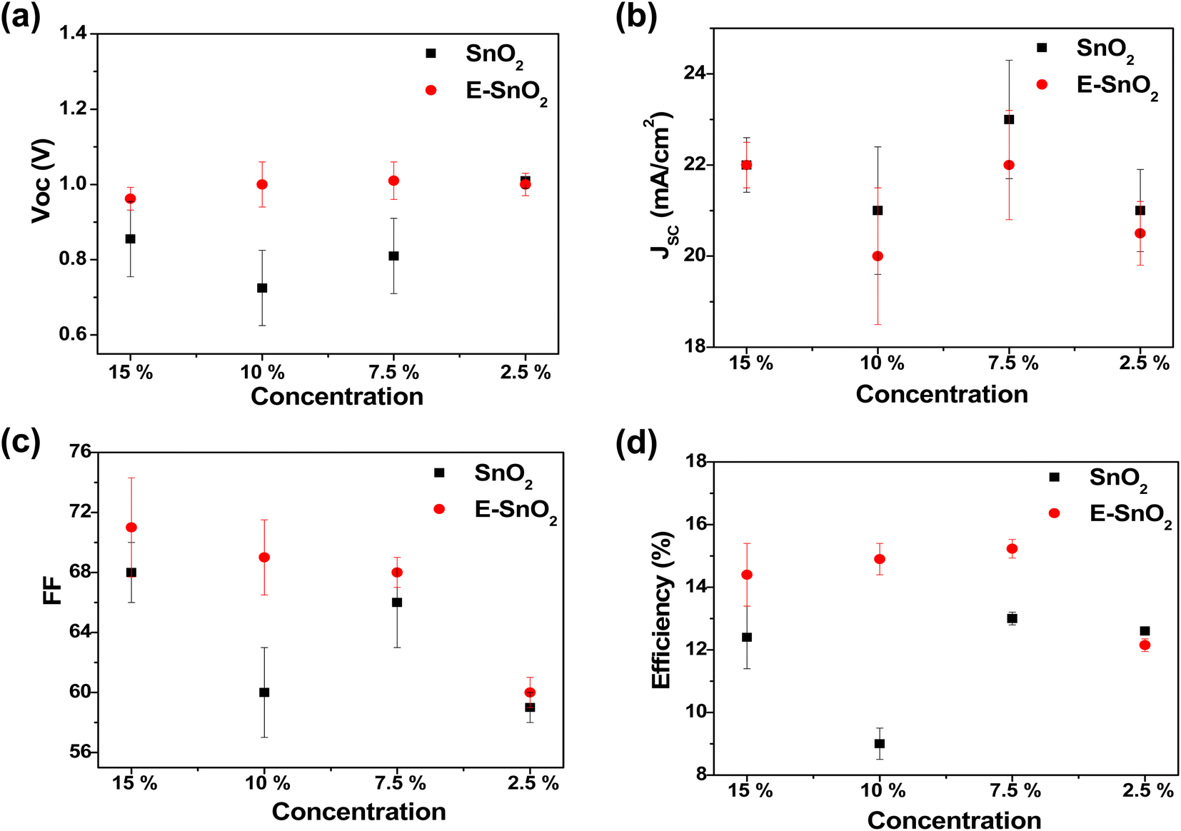
To characterize the effect of E-SnO2 ETLs on perovskite device performance, PSCs were fabricated using the structure of ITO/SnO2 (E-SnO2)/MAPI/spiro-MeOTAD/Au as shown in Fig. 5(a). The cross-sectional SEM image for the corresponding solar cell is shown in Fig. 5(b) with each layer identified for a clearer understanding. The current density–voltage (J–V) curves are used to demonstrate how the device's performance gets better when the combined EDTA based ETL is utilized as a charge transporting layer. We choose only one concentration (7.5%) based ETL which shows the best device performance. The J–V curves for the PSCs with SnO2 (7.5%) and E-SnO2 (7.5%) based ETLs are shown in Fig. 5(c). The electrical measurement of the PSCs shows the values of open-circuit potential (VOC) = 0.82 and 1.015 V, short-circuit current density (JSC) = 24.31 and 22.16 mA cm−2 and fill factor (FF) = 66.5 and 69 for two different cases leading to a PCE of 13.25 and 15.51%, respectively. The improved PCE of the solar cell composed of E-SnO2 is primarily attributed to the enhancement of VOC. This increased VOC from 0.82 V to 1.015 V (∼200 mV) can be explained by the surface passivation that took place after using the EDTA based ETL. The JSC value experiences a decreased value after using E-SnO2 ETL confirmed by the corresponding EQE spectra in Fig. 5(d). The calculation for the JSC values from the EQE spectra is shown in Fig. S1 (ESI†). The stability graph for normalized PCE for both PSCs is shown in Fig. S2.† It shows that after 700 h, the PCE of the E-SnO2 based solar cell decreased ∼17%, while for the SnO2 only based solar cell it decreased ∼38%, which indicates an increase in stability with applying EDTA treatment. Fig. S3† depicts the J–V characteristics for both the reverse and forward scans of the highest-performing PSCs utilizing SnO2 and E-SnO2 ETLs, highlighting the hysteresis behavior of the devices. Additionally, the inset tables provide the performance parameters, including VOC, JSC, FF and PCE for each device configuration. The reduction in hysteresis observed in PSCs employing E-SnO2 as the ETL can be attributed to a lower density of defects at the interface between E-SnO2 and the perovskite layer, compared to the SnO2/perovskite interface. This improvement in interface quality is facilitated by the enhanced surface coverage of the perovskite layer achieved with the E-SnO2 ETL. Fig. 6 shows the photovoltaic characteristics and the distribution of the measured photovoltaic parameters VOC, JSC, FF, and PCE from 10 cells for other different concentration based SnO2 and E-SnO2 based devices. The enhanced VOC and FF for all concentration E-SnO2 based solar cells demonstrate that the presence of small amount of excess PbI2 aids for reducing the defects in the perovskite films which may enhance PSC performance.49–51 For only 15% E-SnO2 based devices, the average value of JSC is higher than that for SnO2 based devices. However, for other concentration, JSC values for E-SnO2 based devices are lower than the SnO2 based devices which might be the cause of excess presence of PbI2 in MAPI. Roose et al.44 also observed that excess PbI2 initially serves to passivate defects and enhance charge carrier dynamics, its photolytic degradation can lead to the creation of additional trap states, thereby offsetting the benefits of its presence. Calloni et al.52 demonstrated that the surface of MAPI undergoes in situ formation of a PbI2 layer during annealing and sputtering. The formation of a thin layer of PbI2 at the crystal surface, which functions as a surface barrier to stop electron transfer from the perovskite film. Kiermasch et al.53 also observed the same characteristics with enhanced lifetime values in solar cells due to bromine doping in MAPbI3 layer. In this case, the effective charge carrier lifetime becomes longer due to a reduction in Shockley–Read–Hall (SRH) recombination. More likely, excess PbI2 in MAPI lattice, acting as dopants for the lattice, creates shallow traps along the conduction band and partially trap the charge carriers, that decreased electron injection into ETL (Fig. S4†). For that reason, the release of charge carriers will slow down which probably reduces the current at short-circuit condition. Therefore, we draw the conclusion that there is a delicate balance between the advantageous and detrimental effects of excess PbI2 in perovskite materials, underscoring the importance of carefully controlling its concentration and stability to optimize PSC performance.
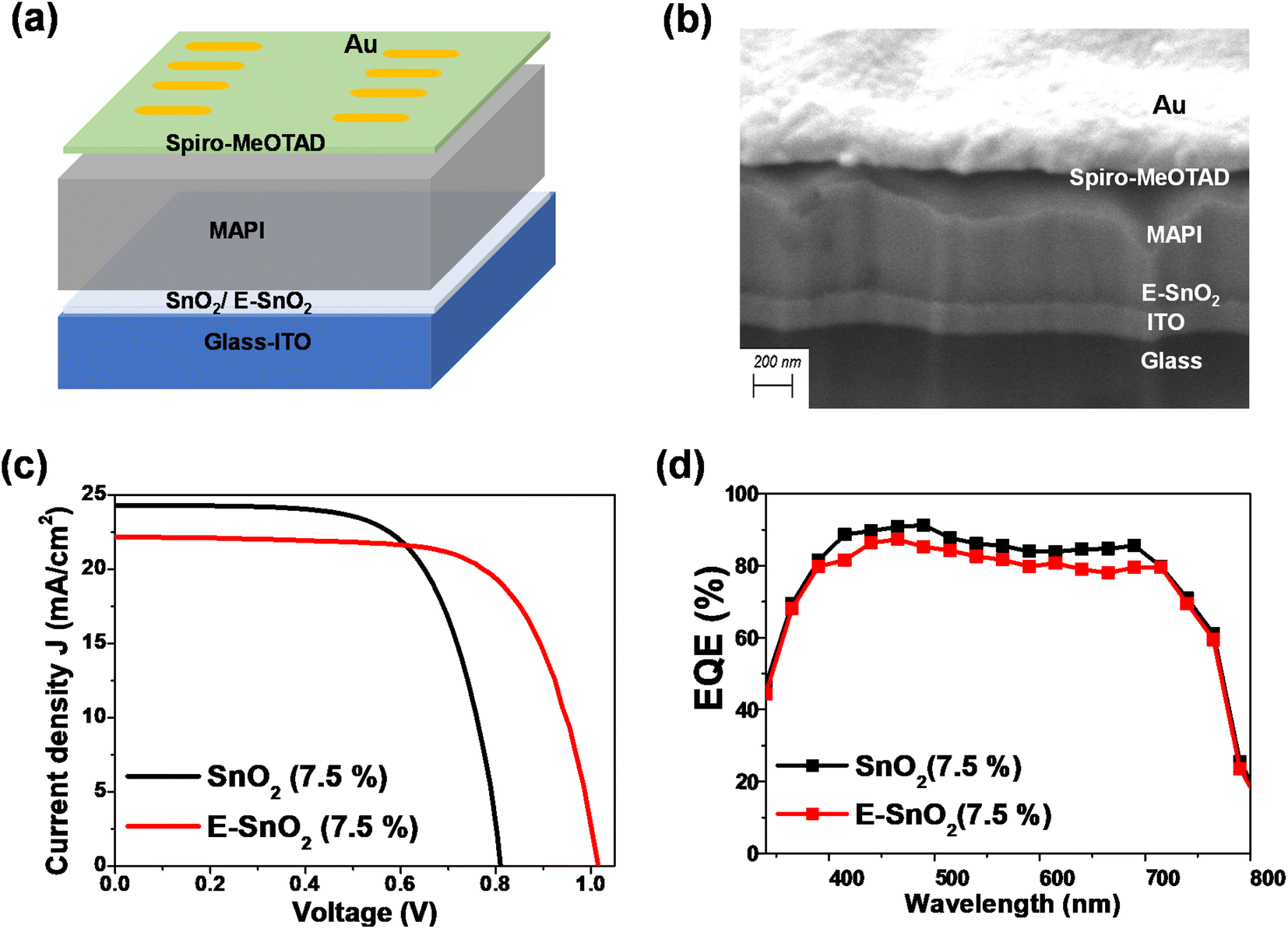 | ||
| Fig. 5 (a) Schematic diagram for the device structure of the PSC. (b) The cross-section SEM image of the PSC on E-SnO2 ETL. (c) Current density–voltage (J–V) curves for the PSCs on SnO2 (7.5%) and E-SnO2 (7.5%) ETLs. (d) Corresponding EQE curves for those cells. | ||
 | ||
| Fig. 6 The distribution of (a) VOC, (b) JSC, (c) FF and (d) PCE for different concentration ETL solution treated PSCs. | ||
To further discuss the above results and provide more insight about the morphology, roughness and conductivity of the ETLs, additional characterizations have been performed. Atomic force microscopy (AFM) topography images of SnO2 (7.5%) and E-SnO2 (7.5%) ETLs are shown in Fig. S5(a) and (b),† respectively. Using Gwyddion software and its row statistical function, we analyzed the surface profiles and calculated the average roughness for SnO2 and E-SnO2 films to be 29.38 nm and 7.38 nm, respectively (Fig. S5c and d†). To know more about the statistical distribution of vertical fluctuations, we collected sixty distinct height profiles from various locations within the topographic images. These profiles were then compiled and utilized to construct plots wherein the width of the distribution corresponds to the surface roughness.54–56 It was observed that the data points were broadly distributed over 11 nm for SnO2, whereas for E-SnO2 the distribution was slightly reduced to 9 nm (Fig. S5e and f†). This observation indicates that the EDTA treatment reduces the roughness of complex E-SnO2 films. This reduction in roughness is a crucial factor in improving the formation of the perovskite layer on E-SnO2, which is essential for achieving high-performance PSCs. In addition, we conducted Hall effect measurements on both types of ETLs to characterize its electron mobility. These measurements provide valuable insights into the charge carrier transport properties of the ETLs, which are critical for understanding its performance in PSCs. Table S1 (ESI†) shows that the E-SnO2 film (7.5%) has an electron mobility of 140 cm3 V−1 s−1, which is much higher than the electron mobility of SnO2 only (36.8 cm3 V−1 s−1). It is clear that the high electron mobility of E-SnO2 facilitates the rapid transport of electrons within the ETL, enabling efficient extraction of photogenerated electrons from the perovskite layer. This helps minimize charge carrier losses and enhances overall device performance. Furthermore, to investigate the reason for the increased of VOC in E-SnO2 based solar cells, we have characterized the surface potentials of the perovskite layers for SnO2 and E-SnO2 based ETLs using Kelvin Probe Force Microscopy (KPFM). The KPFM tip moved easily across the surface of the perovskite layer, measuring the contact potential difference (CPD) between the tip and the sample. Olympus AC240TM probes (details in the experimental part) were used for KPFM measurements.57,58 The AC tip voltage was set to 3 V in a double pass mode in air. The topography and the corresponding surface potential images of the perovskite layers are shown in Fig. 7. Fig. 7(a) and (c) show the topography images, while the corresponding surface potential images are shown in Fig. 7(b) and (d) for the perovskite layers on SnO2 (7.5%) and E-SnO2 (7.5%) ETLs, respectively. KPFM determines the CPD between the tip and sample surface by probing and nullifying the coulomb force between them (Fig. S6†). The CPD is equal to the difference of the work functions between the tip and sample. The quantity of trapped charge carriers at each layer's surface determines the surface potential. As shown by the average CPD plot (Fig. 7(e)) for the two cases, the surface work function of the perovskite film has been significantly modified by the treatment with EDTA. The perovskite on SnO2 has an average potential difference of 230 mV, but the perovskite layer on E-SnO2 has an average potential difference of 370 mV. The perovskite film with higher CPD value on E-SnO2 indicates a reduction in the work function and a rise of the Fermi level, both of which are advantageous for the charge transfer process to separate photogenerated electron–hole pairs, which raises the VOC and FF in PSCs. Therefore, the data presented in above suggests that EDTA treatment plays a crucial and favorable role in modifying the surface characteristics of MAPI, thus improving the functionality of PSCs; where, the current transport is slightly hampered for the excess PbI2 based perovskite layers.
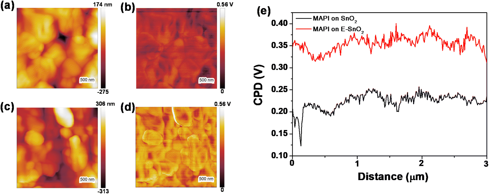 | ||
| Fig. 7 (a and c) Topography and (b and d) corresponding surface potential images for the perovskite films on SnO2 (7.5%) and E-SnO2 (7.5%) ETLs, respectively. (e) Average CPD plot for the corresponding layers. | ||
Conclusion
In this study, we presented a simple and useful strategy that employs EDTA treatment for the surface modification of SnO2 ETL, capable of increasing the performance of planar PSCs. Low temperature deposited E-SnO2 ETLs have shown to improve the properties of the perovskite layer deposited on top, resulting in enhanced PSC efficiency and stability.The enlarged grain size of MAPI for E-SnO2 ETL and the increased CPD values resulted in an improvement in VOC from 0.82 V to 1.015 V, which was the main cause for the enhanced PSC performance. Our findings indicate that an adequate amount of PbI2 in MAPI assists in passivating the polycrystalline film surfaces, owing to the advantageous Pb terminations decreasing the trap densities. Nevertheless, the drawbacks of excessive PbI2 are also assessed. Namely the lower value of JSC attained for the E-SnO2 ETL based PSCs is likely caused by the introduction of shallow defects due to excess PbI2 in MAPI, which decreases the carrier extraction probability from the absorber layer. Lastly, statistical data collected from PSCs showed that devices based on E-SnO2 ETL also benefit from enhanced stability.
Experimental section
Materials
Glass/indium tin oxide (ITO) substrates; SnO2 colloid precursor (15% H2O colloidal dispersion); ethylenediaminetetraacetic acid (EDTA) were utilized for ETL. The MAPI perovskite solution was synthesized utilizing lead(II) iodide (PbI2) and methylammonium iodide (CH3NH3I), dimethylformamide (DMF), and dimethyl sulfoxide (DMSO), all of which were obtained from Sigma-Aldrich. To prepare HTL, a solution of chlorobenzene (C6H5Cl) is mixed with 4-tert-butylpyridine (4-tBP, 96%, Sigma-Aldrich), bis(trifluoromethane) sulfonimide lithium salt (Li-TFSI) (Sigma-Aldrich), and Spiro-MeOTAD (Sigma-Aldrich). The solvents and compounds were utilized without additional purification or treatment.Fabrication of SnO2/E-SnO2 layer and perovskite solar cell
The glass/ITO substrates were successively washed by sonication with soap solution, distilled water, acetone, and isopropanol after the etching process. The substrates were subsequently dried out using compressed air. In addition, the substrates experienced a 15 minute UV–ozone treatment before SnO2/E-SnO2 deposition. SnO2 film is prepared by spin coating on cleaned ITO substrate at 4000 rpm for 30 s and then heated at a temperature of 150 °C for 15 min and 180 °C for 1 h. For making different concentration based SnO2 solution, as purchased SnO2 aqueous colloidal dispersion (15 wt%) was diluted using deionized water to the concentrations of 10, 7.5 and 2.5 wt%. The EDTA solution was prepared by dissolving 1 mg of EDTA in 5 mL of deionized water. Both solutions were stirred for 30 min at room temperature. The EDTA solution was mixed with the SnO2 solutions with a volume ratio of 1![[thin space (1/6-em)]](https://www.rsc.org/images/entities/char_2009.gif) :1 to obtain the E-SnO2 solutions with the corresponding concentrations. These E-SnO2 solutions were then stirred at 80 °C for 5 h. After that, E-SnO2 solutions were spin coated on cleaned ITO substrates at 5000 rpm for 60 seconds and moved to a vacuum oven at 60 °C for 30 minutes to remove the leftover solvent.
:1 to obtain the E-SnO2 solutions with the corresponding concentrations. These E-SnO2 solutions were then stirred at 80 °C for 5 h. After that, E-SnO2 solutions were spin coated on cleaned ITO substrates at 5000 rpm for 60 seconds and moved to a vacuum oven at 60 °C for 30 minutes to remove the leftover solvent.
Prior to the deposition of the perovskite layer, the samples experienced a 15 minute UV–ozone treatment at 150 °C. The spin coating technique was employed to deposit perovskite films in two stages: at 1000 and 5000 rpm for 10 and 30 seconds, respectively, and using a precursor solution combining PbI2 and MAI (molar ratio 1:1) in anhydrous DMF and DMSO. 10 seconds prior to the end of the program, 150 µL of chlorobenzene was dropped onto the substrate in the second phase of the spinning condition. The samples were then annealed at 100 °C for 15 minutes. The HTL was subsequently formed on top of the perovskite layer by spin-coating technique at 3500 rpm for 30 seconds with the solution of Spiro-MeOTAD (40 µL) made with chlorobenzene, LiTFSI stock solution (520 mg of LiTFSI in 1 mL of acetonitrile), and 4-tBP. 100 nm of gold on top of the device was deposited using home made e-beam evaporation technology under high vacuum to operate as a cathode.
Characterizations
SEM (Carl Zeiss AURIGA Cross Beam workstation) and atomic force microscopy (AFM; MFP-3D Infinity atomic force microscope from Oxford Instruments Asylum Research; Santa Barbara, CA) were used to examine the surface morphology and topology of SnO2/E-SnO2 and MAPI layers. Cross-sectional SEM images for devices were obtained by employing a standard ET type secondary electron detector in conjunction with 30 kV Ga+ ions at 20 pA. We used Olympus AC240TM probes for KPFM in an Asylum Research MFP-3D standalone system. The spring constant was 2 N m−1, the resonant frequency was 70 kHz, and the AC tip voltage was 3 V in a double pass mode. Using the Hall measurement system (BiO-RAD/Nanometrics HL5500), the carrier concentration of the different layers had been measured.X-ray diffractometer (Panalytical Xpert PRO system; Cu Kα radiation; λ = 1.5405 Å and X'Celerator 1D detector) was used to know the crystallographic structure of the material. An AXIS Supra+ spectrometer by Kratos Analytical was used for X-ray photoelectron spectroscopy (XPS) examination. The steady-state photoluminescence (PL) spectra was acquired using a high-resolution spectrometer (Horiba Jobin Yvon, Model: iHR 320) together with a photomultiplier tube. The photovoltaic characteristics of PSCs were measured under AM 1.5G illumination using a workstation (Sciencetech SS1.6kW-A-2-Q system with Keithley source meter: Model 2400). A monochromator (Newport) and a Xenon lamp (Newport) were used to assess external quantum efficiency (EQE).
Conflicts of interest
There are no conflicts to declare.Acknowledgements
This work is funded by FCT-MCTES (Fundação para a Ciência e Tecnologia, I. P.) via the postdoctoral grant SFRH/BPD/123502/2016, under the projects LA/P/0037/2020, UIDP/50025/2020 and UIDB/50025/2020 of the Associate Laboratory Institute of Nanostructures, Nanomodelling and Nanofabrication—i3N, and by the projects FlexSolar (PTDC/CTM-REF/1008/2020), SpaceFlex (2022.01610.PTDC) and M-ECO2 (Industrial cluster for advanced biofuel production, Ref. C644930471-00000041) co-financed by PRR - Recovery and Resilience Plan of the European Union (Next Generation EU). This work also received funding from the European Community's H2020 program under the projects DIGISMART (grant agreement no. 787410, ERC-2018-AdG) and SYNERGY (H2020-WIDESPREAD-2020-5, CSA, proposal no. 952169). We acknowledge Jonas Deuermeier and Tomás Calmeiro for their help in XPS and AFM measurements, respectively.References
- J. Y. Kim, J.-W. Lee, H. S. Jung, H. Shin and N.-G. Park, Chem. Rev., 2020, 120, 7867–7918 CrossRef CAS PubMed
.
- J. Gong, Y. Cui, F. Li and M. Liu, Small Sci., 2023, 3, 2200108 CrossRef CAS
- B. C. Karunarathne, S. P. Dunuweera, A. T. Medagedara, D. Velauthapillai, R. Punniamoorthy, A. G. U. Perera, L. A. DeSilva, K. Tennakone, R. M. G. Rajapakse and G. R. A. Kumara, ACS Omega, 2023, 8, 23501–23509 CrossRef CAS PubMed
- E. Couderc, Nat. Energy, 2017, 2, 17080 CrossRef
- S. Panigrahi, S. Jana, T. Calmeiro, D. Nunes, J. Deuermeier, R. Martins and E. Fortunato, J. Mater. Chem. A, 2019, 7, 19811–19819 RSC
- D. B. Straus and R. J. Cava, ACS Appl. Mater. Interfaces, 2022, 14, 34884–34890 CrossRef CAS PubMed
- M. C. Gélvez-Rueda, M. B. Fridriksson, R. K. Dubey, W. F. Jager, W. van der Stam and F. C. Grozema, Nat. Commun., 2020, 11, 1901 CrossRef PubMed
- K. R. Hansen, C. E. McClure, D. Powell, H.-C. Hsieh, L. Flannery, K. Garden, E. J. Miller, D. J. King, S. Sainio, D. Nordlund, J. S. Colton and L. Whittaker-Brooks, Adv. Opt. Mater., 2022, 10, 2102698 CrossRef CAS
- G. W. P. Adhyaksa, L. W. Veldhuizen, Y. Kuang, S. Brittman, R. E. I. Schropp and E. C. Garnett, Chem. Mater., 2016, 28, 5259–5263 CrossRef CAS
- J. Park, J. Kim, H. S. Yun, M. J. Paik, E. Noh, H. J. Mun, M. G. Kim, T. J. Shin and S. I. Seok, Nature, 2023, 616, 724–730 CrossRef CAS PubMed
- S. Panigrahi, M. Sk, S. Jana, S. Ghosh, J. Deuermeier, R. Martins and E. Fortunato, ACS Appl. Energy Mater., 2022, 5, 5680–5690 CrossRef CAS
- S. Haque, M. J. Mendes, O. Sanchez-Sobrado, H. Águas, E. Fortunato and R. Martins, Nano Energy, 2019, 59, 91–101 CrossRef CAS
- S. Haque, M. Alexandre, C. Baretzky, D. Rossi, F. De Rossi, A. T. Vicente, F. Brunetti, H. Águas, R. A. S. Ferreira, E. Fortunato, M. Auf Der Maur, U. Würfel, R. Martins and M. J. Mendes, ACS Photonics, 2022, 9, 2408–2421 CrossRef CAS
- J. Wang, X. Zhou, J. Ni, J. Guan, M. Hu, R. Wang, Y. Zhang, J. Li, H. Cai and J. Zhang, J. Mater. Sci.: Mater. Electron., 2021, 32, 28417–28425 CrossRef CAS
- S. Panigrahi, S. Jana, T. Calmeiro, D. Nunes, R. Martins and E. Fortunato, ACS Nano, 2017, 11, 10214–10221 CrossRef CAS PubMed
- S. Lin, B. Yang, X. Qiu, J. Yan, J. Shi, Y. Yuan, W. Tan, X. Liu, H. Huang, Y. Gao and C. Zhou, Org. Electron., 2018, 53, 235–241 CrossRef CAS
- P. Sun, G. Qu, Q. Hu, Y. Ma, H. Liu, Z.-X. Xu and Z. Huang, ACS Appl. Energy Mater., 2022, 5, 3568–3577 CrossRef CAS
- J. Zhang, C. Bai, Y. Dong, W. Shen, Q. Zhang, F. Huang, C. Bing and J. Zhong, Chem. Eng. J., 2021, 425, 131444 CrossRef CAS
- S.-U. Lee, H. Park, H. Shin and N.-G. Park, Nanoscale, 2023, 15, 5044–5052 RSC
- J.-Y. Chen, C.-C. Chueh, Z. Zhu, W.-C. Chen and A. Jen, Sol. Energy Mater. Sol. Cells, 2017, 164, 47–55 CrossRef CAS
- W. Ke, G. Fang, Q. Liu, L. Xiong, P. Qin, H. Tao, J. Wang, H. Lei, B. Li, J. Wan, G. Yang and Y. Yan, J. Am. Chem. Soc., 2015, 137, 6730–6733 CrossRef CAS PubMed
- N. Chai, X. Chen, Z. Zeng, R. Yu, Y. Yue, B. Mai, J. Wu, L. Mai, Y.-B. Cheng and X. Wang, Natl. Sci. Rev., 2023, 10, nwad245 CrossRef PubMed
- K. Wei, J. Deng, L. Yang, C. Zhang, M. Huang, X. Cai, X. Zhang and J. Zhang, Adv. Energy Mater., 2023, 13, 2203448 CrossRef CAS
- H. Wang, J. Yuan, J. Xi, J. Du and J. Tian, J. Phys. Chem. Lett., 2021, 12, 9142–9148 CrossRef CAS PubMed
- J. Liu, S. Li, S. Liu, Y. Chu, T. Ye, C. Qiu, Z. Qiu, X. Wang, Y. Wang, Y. Su, Y. Hu, Y. Rong, A. Mei and H. Han, Angew Chem. Int. Ed. Engl., 2022, 61, e202202012 CrossRef CAS PubMed
- E. Jiang, J. Yan, Y. Ai, N. Li, B. Yan, Y. Zeng, J. Sheng and J. Ye, Mater. Today Energy, 2019, 12, 389–397 CrossRef
- J. Song, H. Liu, W. Pu, Y. Lu, Z. Si, Z. Zhang, Y. Ge, N. Li, H. Zhou, W. Xiao, L. Wang and M. Sui, Energy Environ. Sci., 2022, 15, 4836–4849 RSC
- Y. Qiang, Y. Xie, Y. Qi, P. Wei, H. Shi, C. Geng and H. Liu, Sol. Energy, 2020, 201, 523–529 CrossRef CAS
- R. Wang, J. Wu, S. Wei, J. Zhu, M. Guo, Q. Zheng, M. Wei and S. Cheng, J. Power Sources, 2022, 544, 231870 CrossRef CAS
- H. Zhou, Y. Yang, X. Li, S. Wu, J. Lu, S. Zhao, D. Wu, W. Xu, P. Chen and L. Zhou, J. Lumin., 2023, 263, 120144 CrossRef CAS
- H. V. Quy and C. W. Bark, ACS Omega, 2022, 7, 22256–22262 CrossRef CAS PubMed
- H. Yi, D. Wang, M. A. Mahmud, F. Haque, M. B. Upama, C. Xu, L. Duan and A. Uddin, ACS Appl. Energy Mater., 2018, 1, 6027–6039 CrossRef CAS
- X. Zhang, Y. Zhou, M. Chen, D. Wang, L. Chao, Y. Lv, H. Zhang, Y. Xia, M. Li, Z. Hu and Y. Chen, Small, 2023, 19, 2303254 CrossRef CAS PubMed
- T. Li, Y. Rui, X. Wang, J. Shi, Y. Wang, J. Yang and Q. Zhang, ACS Appl. Energy Mater., 2021, 4, 7002–7011 CrossRef CAS
- V. Yarangsi, K. Hongsith, S. Sucharitakul, A. Ngamjarurojana, A. Tuantranont, P. Kumnorkaew, Y. Zhao, S. Phadungdhitidhada and S. Choopun, J. Phys. D: Appl. Phys., 2020, 53, 505103 CrossRef CAS
- Y. Gao, Z. He, Q. Geng, X. Jia, S. Zhang and D. Wang, J. Mater. Chem. C, 2023, 11, 14589–14596 RSC
- D. Yang, R. Yang, K. Wang, C. Wu, X. Zhu, J. Feng, X. Ren, G. Fang, S. Priya and S. Liu, Nat. Commun., 2018, 9, 3239 CrossRef PubMed
- M. A. Green, E. D. Dunlop, M. Yoshita, N. Kopidakis, K. Bothe, G. Siefer and X. Hao, Prog. Photovolt. Res. Appl., 2023, 31, 651–663 CrossRef
- R. Keshtmand, M. R. Zamani-Meymian, F. Mohamadkhani and N. Taghavinia, Sol. Energy, 2021, 228, 253–262 CrossRef CAS
- R. Keshtmand, M. R. Zamani-Meymian and N. Taghavinia, Surf. Interfaces, 2022, 28, 101596 CrossRef CAS
- A. P. Muthukrishnan, J. Lee, J. Kim, C. S. Kim and S. Jo, RSC Adv., 2022, 12, 4883–4890 RSC
- T. Cao, K. Chen, Q. Chen, Y. Zhou, N. Chen and Y. Li, ACS Appl. Mater. Interfaces, 2019, 11, 33825–33834 CrossRef CAS PubMed
- X. Li, X. Liu, W. Zhang, H.-Q. Wang and J. Fang, Chem. Mater., 2017, 29, 4176–4180 CrossRef CAS
- B. Roose, K. Dey, Y.-H. Chiang, R. H. Friend and S. D. Stranks, J. Phys. Chem. Lett., 2020, 11, 6505–6512 CrossRef CAS PubMed
- M. Zhu, Z. Sun, M. Fujitsuka and T. Majima, Angew. Chem., Int. Ed., 2018, 57, 2160–2164 CrossRef CAS PubMed
- E. Khorshidi, B. Rezaei, D. Blätte, A. Buyruk, M. A. Reus, J. Hanisch, B. Böller, P. Müller-Buschbaum and T. Ameri, Sol. RRL, 2022, 6, 2200023 CrossRef CAS
- Q. Chen, H. Zhou, T.-B. Song, S. Luo, Z. Hong, H.-S. Duan, L. Dou, Y. Liu and Y. Yang, Nano Lett., 2014, 14, 4158–4163 CrossRef CAS PubMed
- T. Du, C. H. Burgess, J. Kim, J. Zhang, J. R. Durrant and M. A. McLachlan, Sustainable Energy Fuels, 2017, 1, 119–126 RSC
- K. Guo, Energy Rep., 2023, 9, 62–73 CrossRef
- A. Merdasa, A. Kiligaridis, C. Rehermann, M. Abdi-Jalebi, J. Stöber, B. Louis, M. Gerhard, S. D. Stranks, E. L. Unger and I. G. Scheblykin, ACS Energy Lett., 2019, 4, 1370–1378 CrossRef CAS
- Z. Ahmad, R. A. Scheidt, M. P. Hautzinger, K. Zhu, M. C. Beard and G. Galli, ACS Energy Lett., 2022, 7, 1912–1919 CrossRef CAS
- A. Calloni, A. Abate, G. Bussetti, G. Berti, R. Yivlialin, F. Ciccacci and L. Duò, J. Phys. Chem. C, 2015, 119, 21329–21335 CrossRef CAS
- D. Kiermasch, P. Rieder, K. Tvingstedt, A. Baumann and V. Dyakonov, Sci. Rep., 2016, 6, 39333 CrossRef CAS PubMed
- K. Dey, S. Roy Chowdhury, E. Dykstra, H. P. Lu, R. Shinar, J. Shinar and P. Anzenbacher, ACS Appl. Electron. Mater., 2021, 3, 3365–3371 CrossRef CAS
- K. Dey, S. R. Chowdhury, E. Dykstra, A. Koronatov, H. P. Lu, R. Shinar, J. Shinar and P. Anzenbacher, J. Mater. Chem. C, 2020, 8, 11988–11996 RSC
- B. Dhital, V. G. Rao and H. P. Lu, Phys. Chem. Chem. Phys., 2017, 19, 17216–17223 RSC
- S. Panigrahi, T. Calmeiro, R. Martins, D. Nunes and E. Fortunato, ACS Nano, 2016, 10, 6139–6146 CrossRef CAS PubMed
- S. Panigrahi, S. Jana, T. Calmeiro, E. Fortunato, M. J. Mendes and R. Martins, ACS Appl. Mater. Interfaces, 2024, 16, 1930–1940 CrossRef CAS PubMed
Footnote |
| † Electronic supplementary information (ESI) available. See DOI: https://doi.org/10.1039/d3ra08900b |
| This journal is © The Royal Society of Chemistry 2024 |