
 Open Access Article
 This Open Access Article is licensed under a Creative Commons Attribution-Non Commercial 3.0 Unported Licence
Electronic and magnetic properties of GeS monolayer effected by point defects and doping†
Phuong Thuy Buiab,
Vo Van On*c,
J. Guerrero-Sanchezd and
D. M. Hoat *ae
*ae
aInstitute of Theoretical and Applied Research, Duy Tan University, Ha Noi 100000, Vietnam. E-mail: dominhhoat@duytan.edu.vn
bFaculty of Pharmacy, Duy Tan University, Da Nang 550000, Vietnam
cCenter for Forecasting Study, Institute of Southeast Vietnamese Studies, Thu Dau Mot University, Binh Duong Province, Vietnam. E-mail: onvv@tdmu.edu.vn
dUniversidad Nacional Autónoma de México, Centro de Nanociencias y Nanotecnología, Apartado Postal 14, Ensenada, Baja California Código Postal 22800, Mexico
eFaculty of Natural Sciences, Duy Tan University, Da Nang 550000, Vietnam
First published on 12th January 2024
Abstract
In this work, defect engineering and doping are proposed to effectively functionalize a germanium sulfide (GeS) mononolayer. With a buckled hexagonal structure, the good dynamical and thermal stability of the GeS monolayer is confirmed. PBE(HSE06)-based calculations assert the indirect gap semiconductor nature of this two-dimensional (2D) material with a relatively large band gap of 2.48(3.28) eV. The creation of a single Ge vacancy magnetizes the monolayer with a total magnetic moment of 1.99 μB, creating a the feature-rich half-metallic nature. VaS vacancy, VaGeS divacancy, SGe and GeS antisites preserve the non-magnetic nature; however, they induce considerable band gap reduction of the order 47.98%, 89.11%, 29.84%, and 62.5%, respectively. By doping with transition metals (TMs), large total magnetic moments of 3.00, 4.00, and 5.00 μB are obtained with V, Cr–Fe, and Mn impurities, respectively. The 3d orbital of TM dopants mainly regulates the electronic and magnetic properties, which induces either the half-metallic or diluted magnetic semiconductor nature. It is found that the doping site plays a determinant role in the case of doping with VA-group atoms (P and As). The GeS monolayer can be metallized by doping the Ge sublattice, meanwhile both spin states exhibit semiconductor character with strong spin polarization upon doping the S sublattice to obtain a diluted magnetic semiconductor nature with a total magnetic moment of 1.00 μB. In these cases, the magnetism originates mainly from P and As impurities. The obtained results suggest an efficient approach to functionalize the GeS monolayer for optoelectronic and spintronic applications.
1. Introduction
For many years, the number of transistors per chip in the electronics industry followed Moore's law, that is, it doubled every two years.1 Nowadays, Moore's law is gradually losing its effects for conventional electronics based on electron charge, due to the demand of new alternatives with low energy consumption and high processing speed. In this regard, different solutions have explored including nanoelectronics,2,3 molecular electronics,4,5 and spintronics.6,7 Between them, spintronics or spin-based electronics emerges as a promising solution rapidly replacing silicon-based electronics, in which the electron is counted as an additional degree of freedom (rather than its charge) for information storage and processing. The era of spintronics started with the discovery of the giant magnetoresistive effects (GMR) in 1988 in a thin-film two-layered material composed of one ferromagnetic layer and the other non-magnetic, whose resistance can be controlled by aligning the magnetic moments.8,9 Besides, the identification of tunnel magnetoresistance (TMR) is also marked as an important milestone for the development of spintronics, which occurs in a magnetic tunnel junction composed of two ferromagnetic layers separated by one semiconductor or insulator layer. Herein, the resistance of the material exhibits significant change due to the application of the external magnetic field.10,11 So far, different devices based on spintronic phenomena have been fabricated as spin photodiodes,12,13 spin field-effect transistors,14,15 and spin LED.16,17 The development of spintronics has been extended past Moore's law. One of the biggest challenges of this field is the generation of fully spin-polarized carriers, therefore great effort in both scientific research and industry has been made to develop new spintronic materials, where half-metallic and diluted magnetic semiconductor candidates have gained special attention.18,19It is well known that materials exhibit novel properties different from their bulk counterparts, when thinned to their physical limits. Since the discovery of graphene,20 researchers have exploited two-dimensional (2D) materials for a wide range of applications as electronics and optoelectronics,21,22 catalysis,23,24 energy storage,25,26 gas sensing,27,28 biomedical and environment,29,30 and spintronics.31,32 To date, 2D materials such as graphene,33 silicene,34 phosphorene,35 and transition metal dichalcogenides (TMDs),36 provide excellent platforms for spintronic nanodevices. However, these 2D candidates are mostly non-magnetic, such that a spin injection process is needed which may affect the polarization efficiency.37,38 Therefore, different solutions have been developed including magnetic engineering,39,40 and seeking new magnetic 2D materials containing transition metals or earth rare metals.41,42 The former approach has been widely investigated through defect engineering and doping, which has lead to the emergence of novel magnetism with feature-rich half-metallicity or diluted magnetic semiconducting in non-magnetic 2D materials suitable for spintronic applications. Experimentally, high-energy ion or atom bombardment is employed to create defects and realize further doping.43,44
Stimulated by the increasingly fast growth of research on 2D materials, group-IV monochalcogenides semiconductor monolayers have been investigated by various research groups45,46 using first-principles calculations. Between them, the germanium sulfide (GeS) monolayer is found to possess high carrier mobility,47 giant piezoelectricity,48 and low thermal conductivity.49 However, most investigations consider the black phosphorene-like structure, while the buckled hexagonal configuration has not been predicted despite its versatility for a large variety of 2D materials. In this work, the buckled hexagonal GeS monolayer with good structural stability is predicted. It is anticipated that this 2D material is a non-magnetic indirect gap semiconductor with relatively large band gap, therefore point defects and doping are proposed as efficient functionalization approaches. Significant magnetism with feature-rich half-metallic or diluted magnetic semiconductor nature as well as band gap reduction, can be achieved to make the GeS mononolayer more suitable for optoelectronic and spintronic applications.
2. Computational details
First-principles calculations are performed using the Vienna ab initio simulation package (VASP),50,51 implementing density functional theory (DFT).52 the electron exchange-correlation potential is treated within the Generalized Gradient Approximation of the Perdew–Burke–Enzerhof (GGA-PBE),53 while the projector augmented wave (PAW) method describes the electron–ion interactions. In order to get a proper description of 3d electrons, the DFT + U approach54 is adopted. Herein, effective Hubbard parameter Ueff values of 3.25, 3.70, 3.90, and 5.40 eV are employed for V, Cr, Mn, and Fe transition metals, respectively, which have been used previously by various research groups.55 The plane wave basis is truncated with a cutoff energy of 500 eV. The self-consistency criterion for energy is set to 10−6 eV. For structural relaxation, the Hellmann–Feynman forces are less than 0.01 eV Å−1. A Monkhorst–Pack k-mesh56 of 20 × 20 × 1 is generated to sample the first Brillouin zone of the unit cell, while that of a 4 × 4 × 1 supercell is integrated with the k-grid of 4 × 4 × 1. The electronic band structures are calculated along the M–Γ–K–M direction, which can be generated using the AFLOW code at https://aflowlib.org/aflow-online/.57 The vacuum thickness larger than 14 Å is inserted along the z axis perpendicular to the monolayer plane, which is large enough to avoid the interactions between adjacent layers.Using the small displacement method as embedded in PHONOPY code,58 a 4 × 4 × 1 supercell is generated to calculate the phonon dispersion curves of the GeS monolayer. In addition, Ab Initio Molecular Dynamic (AIMD) simulations are also performed to verify its thermal stability using the canonical ensemble NVT (Nose–Hoover thermostat).
The effects of point defects and doping are investigated using a 4 × 4 × 1 supercell, which is large enough to minimize the interactions between defects/impurities. A single vacancy is modelled by removing a Ge or S atom, while the doping is generated by filling the vacancy with a foreign atom. These cases correspond to a defect/dopant concentration of 6.25%. Details of all the relaxed structures are given in the ESI file.† The formation energy of defects Ef as well as doping energy Ed are calculated as follows:
| Ef/d = Et − EGeS + μra − μia | (1) |
 | (2) |
3. Results and discussion
3.1 Stability and electronic properties of a pristine GeS monolayer
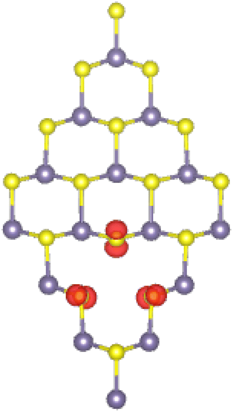
As a starting point, the stability of a GeS monolayer in the buckled honeycomb structure is examined. Fig. 1a shows a 4 × 4 × 1 supercell with 16 Ge atoms and 16 S atoms, each hexagonal ring is formed of three alternating Ge atoms and three S atoms. A unit cell contains two inequivalent atoms (one Ge atom and one S atom), which is described using the following parameters obtained from the structural relaxation: (1) lattice constant a = b = 3.49 Å; (b) buckling height ΔGe–S = 1.36 Å; (3) chemical bond length dGe–S = 2.43 Å; and (4) interatomic angles ∠GeSGe = ∠SGeS = 91.69°. The GeS monolayer structural wrinkle is confirmed by either significant buckling height or an interatomic angle different to 120° (despite the constituent atoms forming the honeycomb arrangement). With two atoms in the primitive cell, phonon dispersion curves of the GeS monolayer are composed of six modes (see Fig. 1b). Phonon calculations yield no imaginary phonon frequency around the Γ point, indicating that the GeS monolayer is dynamically stable. To further verify its thermal stability, ab initio molecular dynamic (AIMD) simulations are also performed at 300 K for 5 ps. From Fig. 1c, regular and small fluctuations of temperature and energy can be noted during simulations, suggesting the good thermal stability of the GeS monolayer. Moreover, the visualization of the structure after 5 ps of simulation demonstrates the preservation of the initial configuration without any structural destruction.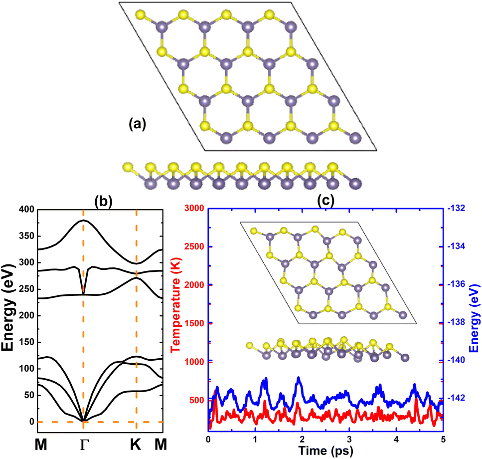 | ||
| Fig. 1 (a) Atomic structure (Ge atom: violet ball; S atom: yellow ball), (b) phonon dispersion curve, and (c) AIMD simulation at 300 K (inset: atomic structure after 5 ps) for the GeS monolayer. | ||
Once the structural stability is verified, the GeS monolayer electronic properties were investigated. Fig. 2 shows the calculated band structure, projected density of states (PDOS), and charge density distribution. From panel (a), one can observe a forbidden energy region formed by the valence band maximum along the ΓK direction and conduction band minimum along the MΓ direction. This feature indicates the indirect gap semiconductor character of the GeS monolayer. The standard PBE and hybrid HSE06 functional, yield an energy gap of 2.48 and 3.28 eV, respectively. Because of the 25% fraction of the exact Hartree exchange potential,59 HSE06 may provide a more accurate electronic band gap of the GeS monolayer, such that 3.28 eV is expected to be close to the experimental value. The PDOS spectra in panel (b) indicate that in the energy range −4 to 6 eV, Ge-4s, Ge-4p, and S-3p orbitals are the main components of the band structure. The upper part of the valence band is constructed mainly of Ge-s, Ge-pz, and S-pz states. The lower part of the conduction band originates mainly from the px, py, and pz states of both constituent atoms. The PDOS profile suggests significant electronic hybridization between the Ge and S atoms, consequently their chemical bond is predominantly covalent. This feature is further confirmed by the charge density illustrated in panel (c), where a large charge quantity is accumulated at the Ge–S bridge. However, the ionic character should not be ignored due to the directionality of charge distribution towards the S atom, due to its more electronegative nature. The Bader charge analysis asserts that a charge quantity of 0.70e is transferred from the Ge atom to the S atom, following the rule of electronegativity.
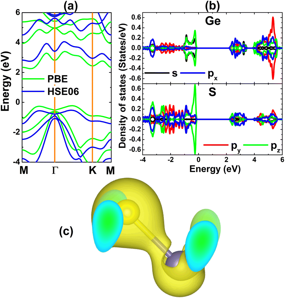 | ||
| Fig. 2 (a) Electronic band structure (the Fermi level is set to 0 eV), (b) projected density of states, and (c) charge density distribution (iso-surface value: 0.05 e Å−3) of the GeS monolayer. | ||
3.2 Effect of point defects
Herein, different point defects in the GeS monolayer are investigated, which are denoted as follows: (1) VaGe: single Ge vacancy; (2) VaS: single S vacancy; (3) VaGeS: Ge + S divacancy; (4) SGe: antisite defect formed by replacing one Ge atom by one S atom; and (5) GeS: antisite defect formed by replacing one S atom by one Ge atom. The calculated formation energies are given in Table 1. Note that the formation of the SGe defect is energetically most favorable with an Ef value of 1.92 eV, while creating the VaGeS divacancy is most difficult, requiring the supply of the largest additional energy of 3.13 eV. In addition, negative cohesive energies between −3.70 and −3.66 eV per atom indicate that the systems with defects are structurally and chemically stable. It is worth mentioning that these values are slightly less negative than that of the pristine monolayer (−3.75 eV), suggesting a slight reduction of the structural-chemical stability after creating point defects in the GeS monolayer.| Ef | Ec | Eg | Mt | |
|---|---|---|---|---|
| VaGe | 2.55 | −3.67 | 2.27/M | 1.99 |
| VaS | 2.23 | −3.69 | 1.29/1.29 | 0.00 |
| VaGeS | 3.13 | −3.66 | 0.27/0.27 | 0.00 |
| SGe | 1.92 | −3.67 | 1.74/1.74 | 0.00 |
| GeS | 2.13 | −3.70 | 0.93/0.93 | 0.00 |
Fig. 3 shows the calculated band structures of the GeS monolayers with defects. From the figure, one can see the spin polarization (mostly at the upper part of the valence band and lower part of the conduction band) of the VaGe system, meanwhile the band structures are spin-symmetric (without spin polarization) in the remaining cases. According to our simulations, the half-metallic nature is induced by a single Ge vacancy generated by a semiconductor spin-up state with an energy gap of 2.27 eV and metallic spin-down state. Despite preserving the non magnetic nature of the GeS monolayer, the creation of other defects effectively tunes the electronic band gap. Specifically, gap values of 1.29, 0.27, 1.74, and 0.93 eV are obtained for VaS, VaGeS, SGe, and GeS system, respectively. These values correspond to a reduction of the order of 47.98%, 89.11%, 29.84% and 62.5% from that of the perfect monolayer, respectively. Note that the band gap reduction is derived from the appearance of new middle-gap states around the Fermi level.
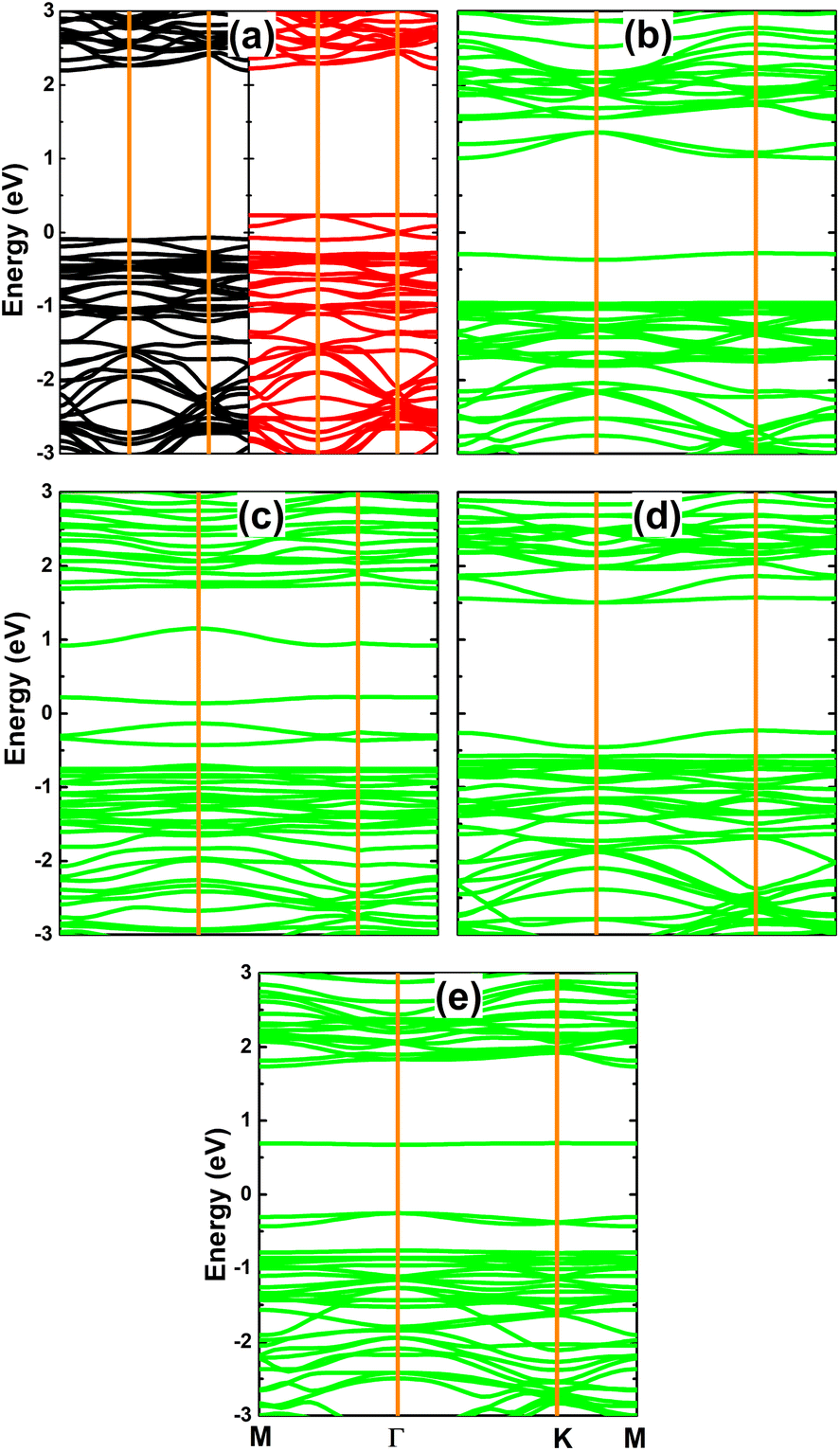 | ||
| Fig. 3 Spin-polarized band structure (the Fermi level is set to 0 eV; black curve: spin-up state; red curve: spin-down state; green curve: non spin polarization) of the GeS monolayer with point defect types: (a) VaGe, (b) VaS, (c) VaGeS, (d) SGe, and (e) GeS. | ||
The total and atom-decomposed density of states (DOS) of the systems with defects are displayed in Fig. 4.
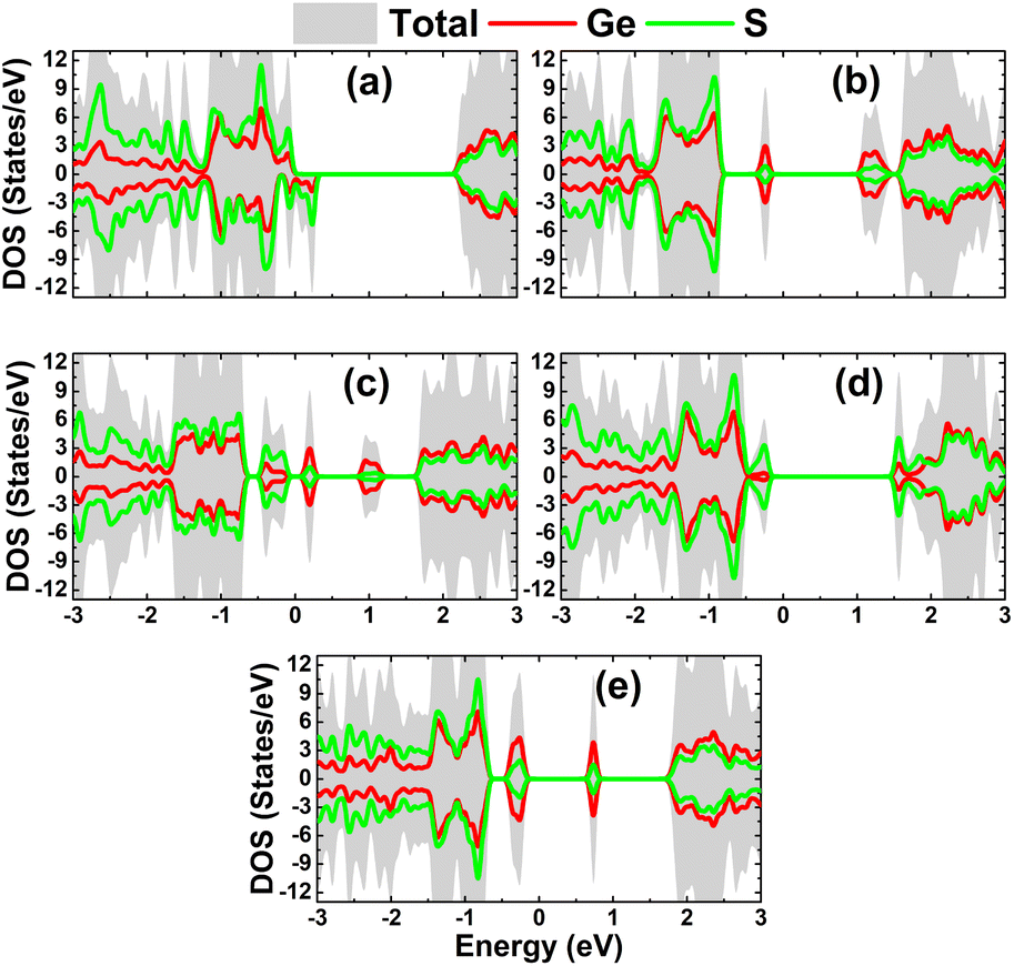 | ||
| Fig. 4 Total and atom-decomposed density of states of the GeS monolayer with point defect types: (a) VaGe, (b) VaS, (c) VaGeS, (d) SGe, and (e) GeS. | ||
Undoubtedly, the electronic modification is derived from the interactions of atoms around the defect sites:
1. The spin-down state metallization of the VaGe system is attributed to S atoms.
2. The band gap of VS and GeS systems is determined mainly by the Ge atoms since their electronic states dominate the upper part of the valence band and lower part of the conduction band (new middle-gap states).
3. The upper part of the valence band and lower part of the conduction band of the VaGeS system are formed by S and Ge atoms, respectively.
4. The electronic properties of the SGe system are regulated mainly by S atoms that form new middle-gap electronic states around the Fermi level.
Spin-polarized band structure and DOS spectra give evidence to the GeS monolayer magnetization induced by a single Ge vacancy, which is confirmed by a total magnetic moment of 1.99 μB. Fig. 5 illustrates the spin density in the VaGe system. Note that the spin surfaces are centered mainly at the S atoms around the vacancy site, indicating the key role of these atoms in magnetizing the GeS monolayer. Further calculations of projected density of states (PDOS) of the S atoms closest to the defect site indicate that the magnetism originates mainly from the S-pz state, which is also responsible for the spin-down state metallization (see Fig. 6).
 | ||
| Fig. 5 Spin surface (iso-surface value: 0.01 e Å−3) in GeS monolayer with a single Ge vacancy. | ||
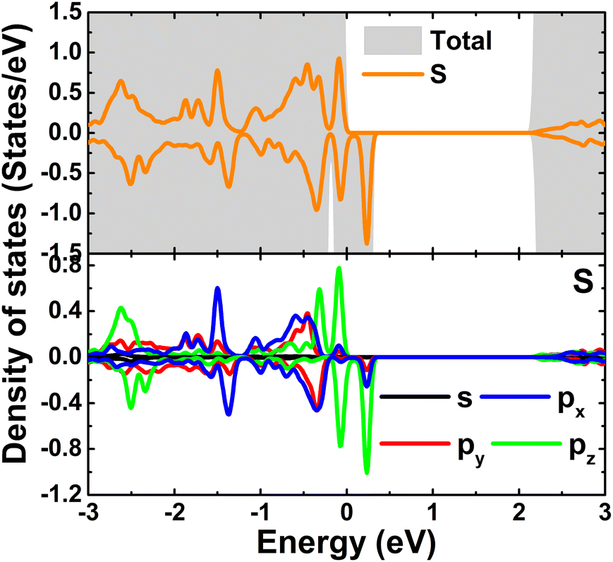 | ||
| Fig. 6 Projected density of states of S atoms closest to the defect site in the GeS monolayer with single Ge vacancy. | ||
3.3 Effects of doping with transition metals
In this part, the effect of doping the GeS monolayer with transition metals (TMs = V, Cr, Mn, and Fe) is investigated. TMGe notation refers to the case of doping the Ge site with a TM. The calculated doping energies are listed in Table 2. Negative Ed values indicate the exothermic process of doping with V (−0.09 eV) and Cr (−0.51 eV), while doping with Mn and Fe are endothermic processes as suggested by the positive doping energies of 0.01 and 1.07 eV, respectively. Cr doping is energetically most favorable due to a most negative doping energy, meanwhile Fe doping requires the largest additional energy of 1.07 eV. The calculated cohesive energies exhibit slight variation between −3.75 and −3.67 eV, where its negative feature implies the good structural-chemical stability of the GeS monolayer doped with transition metals.| Ed | Ec | Eg | ΔQ | Mt | |
|---|---|---|---|---|---|
| VGe | −0.09 | −3.75 | 1.55/2.4 | +1.10 | 3.00 |
| CrGe | −0.51 | −3.67 | M/2.46 | +0.96 | 4.00 |
| MnGe | 0.01 | −3.69 | 2.01/2.39 | +1.02 | 5.00 |
| FeGe | 1.07 | −3.72 | 2.26/M | +0.85 | 4.00 |
| PGe | 1.61 | −3.69 | M/M | +0.56 | 0.00 |
| PS | 1.55 | −3.71 | 1.94/0.85 | −0.51 | 1.00 |
| AsGe | 1.52 | −3.68 | M/M | +0.55 | 0.84 |
| AsS | 1.54 | −3.70 | 1.91/0.74 | −0.31 | 1.00 |
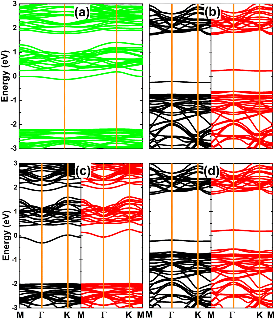
Fig. 7 shows the calculated spin-polarized band structures of TMs-doped GeS monolayers. Note that all the TMs impurities induce significant spin polarization with the appearance of new middle-gap energy states around the Fermi level. It is found that V and Mn doping lead to the emergence of the diluted magnetic semiconductor nature with semiconductor behavior in both spin channels. The spin-up/down energy gaps are 1.55/2.40 and 2.01/2.39 eV, respectively. Meanwhile, one of the spin states is metallized by doping with Cr and Fe, and the semiconductor character is preserved in the other one with a band gap of 2.46 and 2.26 eV, respectively. The band structures profile implies that Cr- and Fe-doped GeS monolayers are half-metallic 2D materials with perfect spin polarization of 100%. Results suggest that TMs doping is an efficient way to induce feature-rich diluted semiconductor and half-metallic nature in the GeS monolayer, which are suitable for spintronic applications.60,61 Once incorporated in the GeS monolayer, transition metals may undergo charge loss, transferring charge to the host monolayer (mostly to S atoms closest to the doping site). This feature is confirmed by the Bader charge analysis, where results assert the transfer of 1.10, 0.96, 1.02, and 0.85e from V, Cr, Mn, and Fe impurities, respectively. The charge transfer may generate an ionic chemical bond between transition metals and their neighbor S atom, which is further investigated by the electron localization function (see the illustrations in Fig. S1 of the ESI file†). Results show a void in the region between TMs impurities and their neighbor atoms. In other words, there is a negligible electron localization in the region between TMs and their neighbor, indicating that the TM-S chemical bonds are predominantly ionic.
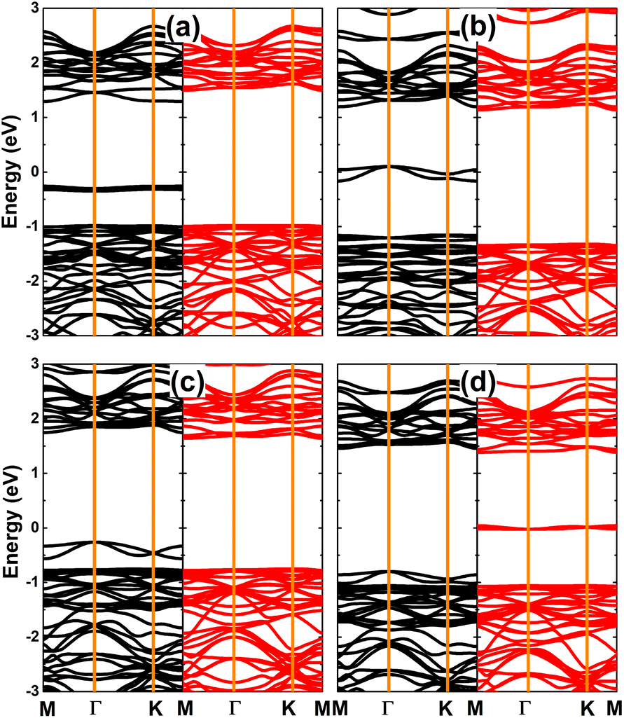 | ||
| Fig. 7 Spin-polarized band structure (the Fermi level is set to 0 eV; black curve: spin-up state; red curve: spin-down state) of (a) V-, (b) Cr-, (c) Mn-, and (d) Fe-doped GeS monolayer. | ||
Highly spin-polarized band structures evidence the magnetization of the GeS monolayer induced by doping with transition metals. According to our simulations, total magnetic moments of 3.00, 4.00, and 5.00 are obtained in the V-, Cr(Fe)-, and Mn-doped systems, respectively. Results indicate the emergence of significant magnetism, whose origin is further investigated by the illustration of spin density and the PDOS spectra of magnetizing atoms in the systems as follows:
1. Fig. 8 illustrates the spin density in a TM-doped GeS monolayer. Note that spin surfaces are centered mainly at TMs sites, indicating that magnetic properties are produced mainly by V, Cr, Mn, and Fe impurities.
2. The DOS spectra displayed in Fig. 9 show that TMs impurities generate new middle-gap electronic states around the Fermi level. Specifically, V-dz2–dxz–dx2 and Mn-dxy–dx2 states are responsible for the spin-up band gap reduction in V- and Mn-doped systems, respectively. In the remaining cases, the spin-dependent metallization is induced by Cr-dxy–dxz–dx2 and Fe-dxz–dx2 states. The spin polarization in PDOS spectra evidence that magnetism is produced mainly by the TMs-3d orbital, indicating its key role in regulating the TMs-doped GeS monolayer electronic and magnetic properties.
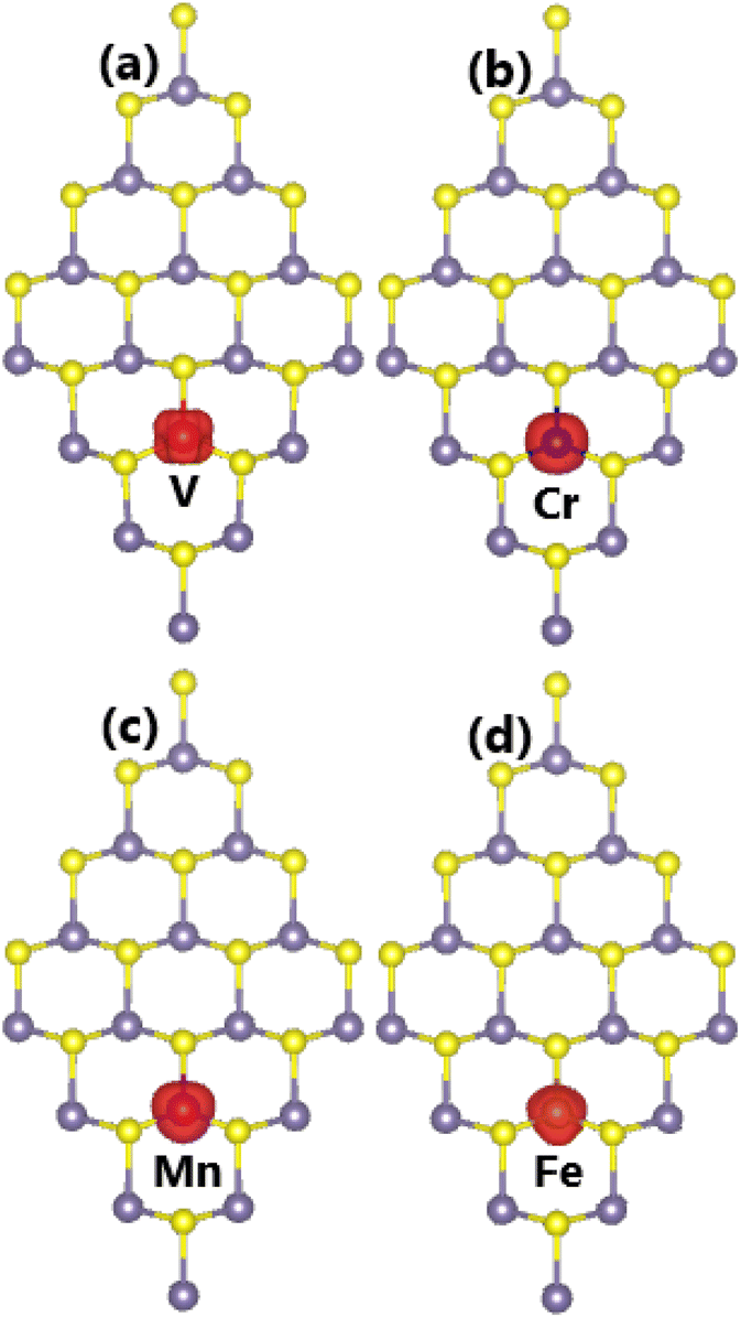 | ||
| Fig. 8 Spin surface (iso-surface value: 0.02 e Å−3) in (a) V-, (b) Cr-, (c) Mn-, and (d) Fe-doped GeS monolayer. | ||
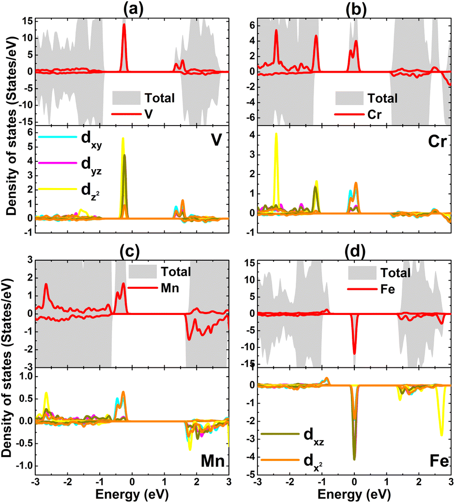 | ||
| Fig. 9 Total and projected density of states of transition metal impurities in (a) V-, (b) Cr-, (c) Mn-, and (d) Fe-doped GeS monolayer. | ||
3.4 Effects of doping with VA-group atoms
Next, GeS monolayers doped with VA-group or pnictogen atoms (P and As) are investigated, where doping at both Ge and S sublattices are considered for n- and p-doping, respectively. The systems are denoted as follows: (1) PGe: doping with P atom at Ge site; (2) PS: doping with P atom at S site; (3) AsGe: doping with As atom at Ge site; and (4) AsS: doping with As atom at S site. From Table 2, one can see that doping with the P atom at the Ge site requires slightly smaller energy than doping at the S site (1.61 eV in comparison with 1.55 eV), meanwhile As doping exhibits the opposite trend (1.52 eV compared to 1.54 eV). Once formed, the doped systems may have good structural-chemical stability as suggested by their negative cohesive energy between −3.71 and −3.68 eV per atom.Fig. 10 shows the calculated band structures of the GeS monolayers doped with P and As atoms. Our calculations evidence the emergence of new middle-gap flat energy branches induced by doping with pnictogen atoms. The GeS monolayer is metallized by doping with the P atom in the Ge sublattice, where no spin polarization is obtained. In contrast, significant spin polarization takes place in the remaining cases with the emergence of new middle-gap energy states around the Fermi level. The band structure profile indicates the diluted magnetic semiconductor nature of PS and AsS systems, where spin-up/down energy gaps of 1.94/0.85 and 1.91/0.74 eV are obtained, respectively. Note that the spin-down values are considerably smaller than the spin-up ones, which is a result of the new spin-down energy state in the lower part of the conduction band close to the valence band maximum. Meanwhile, the metallization is observed in both spin states of the AsGe system. Undoubtedly the interactions between the VA-group impurities and the host GeS monolayer play a key role in the ground state properties of the doped systems. The Bader charge analysis indicates the dopant role of the charge loss when doping at the Ge sublattice, and of charge gain when doping at the S sublattice. Specifically, P and As impurities transfer charge quantities of 0.56 and 0.55e to the GeS monolayer when they are incorporated at the Ge site, respectively. Meanwhile, they gain charge of 0.51 and 0.31e, respectively, when replacing the S atom in the GeS monolayer. The calculated electron localization function indicates that P–S (in PGe system) and As–S (in AsGe system) chemical bonds are predominantly ionic, where small electron localization between P(As) and S atoms suggests a small portion of covalent character (see Fig. S2† of the ESI file†). The covalent character becomes stronger in P–Ge (in the PS system) and As–Ge (in the AsS system) chemical bonds considering the accumulation of electrons in the bridge regions, such that they can be classified as covalent bonds.
 | ||
| Fig. 10 Spin-polarized band structure (the Fermi level is set to 0 eV; black curve: spin-up state; red curve: spin-down state; green curve: non spin polarization) of (a) P- (at the Ge site), (b) P- (at the S site), (c) As- (at the Ge site), and (d) As-doping (at the S site) of the GeS monolayer. | ||
The spin-symmetric band structure suggests no magnetism in the PGe system, meanwhile the spin polarization may show significant magnetization in the GeS monolayer by doping with the P atom at the S sublattice and with the As atom at both sublattices. These features are confirmed by total magnetic moments of 0.00, 1.00, 0.84, and 1.00 μB for PGe, PS, AsGe, and AsS system, respectively. Further, the spin density is calculated to gain insight into the origin of magnetism. The results illustrated in Fig. 11 assert that magnetic properties are produced mainly by P and As impurities considering large spin surfaces centered at their sites, where the contribution of their neighbor is quite small.
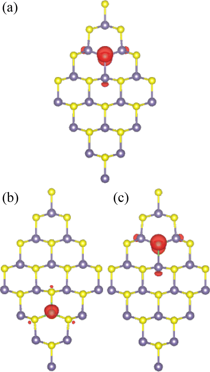 | ||
| Fig. 11 Spin surface (iso-surface value: 0.005 e Å−3) of (a) P- (at the S site), (b) As- (at the Ge site), and (c) As-doped (at the S site) of the GeS monolayer. | ||
To analyze in more detail, the contribution of P and As impurities, their PDOS spectra are given in Fig. 12. It can be seen that they make a significant contribution to both the valence band and conduction band of the doped systems. Most importantly, they produce new middle-gap energy states to regulate the ground state electronic and magnetic properties of the doped systems. Note that the s and pz states of impurities are responsible for the metallic nature in the PGe and AsGe systems. Meanwhile, the spin-dependent electronic band gaps of the PS and AsS systems are determined by the P-pz state that generates both flat energy branches at the vicinity of the Fermi level. From the figures, it can also be concluded that magnetic properties are produced by P-pz and As-pz states in all cases, where a small contribution to the AsGe system magnetism comes also from the As-s state.
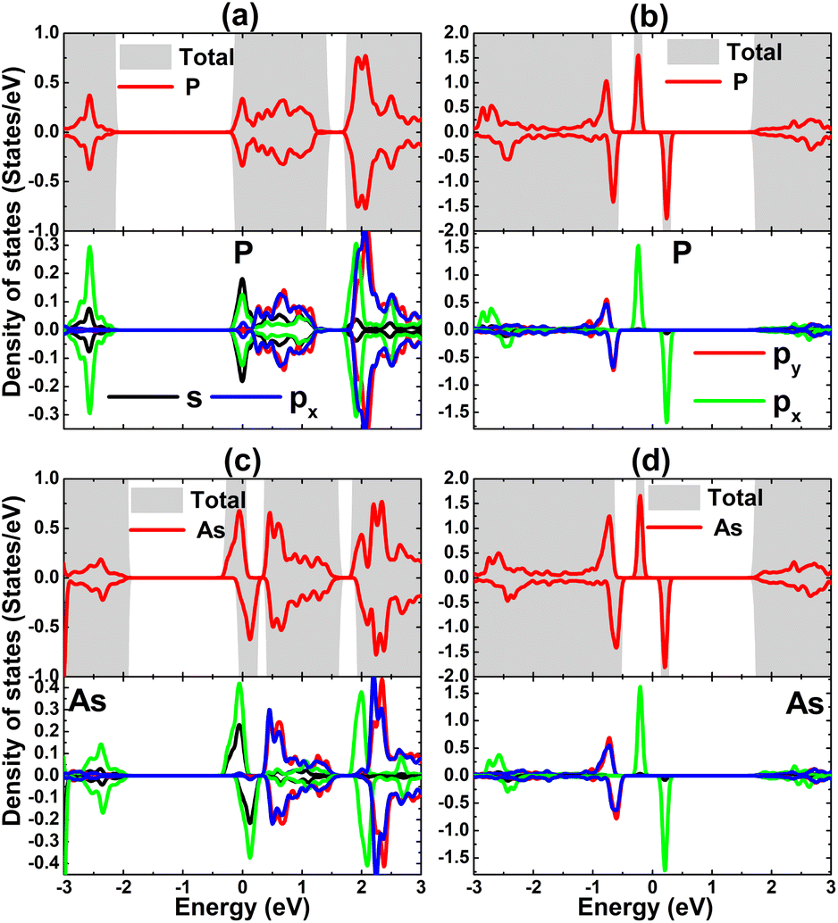 | ||
| Fig. 12 Total and projected density of states of VA-group impurities of P- (at the Ge site), (b) P- (at the S site), (c) As- (at the Ge site), and (d) As-doped (at the S site) of the GeS monolayer. | ||
4. Conclusions
In summary, the electronic and magnetic properties of pristine, defect, and doped buckled honeycomb germanium sulfide monolayer have been systematically investigated using first-principles calculations. The good dynamical and thermal stability of the GeS single layer is confirmed by the calculated phonon dispersion curves and AIMD simulations, respectively. The VaGe defect induces half-metallicity with a total magnetic moment of 1.99 μB, where magnetic properties are produced mainly by the pz state of the S atoms closest to the vacancy site. Meanwhile, other defects including VaS, VaGeS, SGe, and GeS preserve the non-magnetic nature of the GeS monolayer. However, they make new electronic states at the vicinity of the Fermi level as a result of the interactions between atoms around the defect sites. Consequently, the electronic band gap is considerably reduced, which may favor the harvesting of light in a wider regime. Either half-metallic or diluted magnetic semiconductor natures are achieved by doping with transition metals (V, Cr, Mn, and Fe), where magnetism originates mainly from the 3d orbital of the impurities. Moreover, n- and p-doping are also considered by doping P/As atoms at the Ge and S sublattice, respectively. Acting as a charge donor, P and As impurities metallize the GeS monolayer. Meanwhile, the diluted magnetic nature is obtained by p-doping, where the dopants are charge acceptors. The PS-AsS and AsGe systems have total magnetic moments of 1.00 and 0.84 μB, respectively, whose electronic and magnetic properties are regulated mainly by the s and pz states of pnictogen impurities. The results presented herein may introduce defect and doped systems as promising 2D candidates for nano-optoelectronics and nano-spintronics, where defects engineering and doping are proposed to efficiently functionalize the GeS monolayer.Data availability
Data available on request from the authors.Conflicts of interest
The authors declare that they have no known competing financial interests or personal relationships that could have appeared to influence the work reported in this paper.Acknowledgements
Calculations were performed at the DGCTIC-UNAM Supercomputing Center (projects LANCAD-UNAM-DGTIC-368) and the high-performance computing cluster (HPCC) of Thu Dau Mot University (TDMU). Phuong Thuy Bui and D. M. Hoat express their gratitude to all the valuable support from Duy Tan University, which is going to celebrate the 30th anniversary of its establishment (Nov. 11, 1994–Nov. 11, 2024) towards “Integral, Sustainable and Stable Development”.References
- R. R. Schaller, Moore's law: past, present and future, IEEE Spectrum, 1997, 34(6), 52–59 Search PubMed.
- A. Zhang and C. M. Lieber, Nano Bioelectron., 2016, 116(1), 215–257 CAS.
- W. Lu and C. M. Lieber, Nanoelectronics from the bottom up, Nat. Mater., 2007, 6(11), 841–850 CrossRef CAS PubMed.
- C. A. Mirkin and M. A. Ratner, Annu. Rev. Phys. Chem., 1992, 43(1), 719–754 CrossRef CAS.
- R. L. Carroll and C. B. Gorman, The genesis of molecular electronics, Angew. Chem., Int. Ed., 2002, 41(23), 4378–4400 CrossRef PubMed.
- S. D. Bader and S. Parkin, Annu. Rev. Condens. Matter Phys., 2010, 1(1), 71–88 CrossRef CAS.
- S. Wolf, D. Awschalom, R. Buhrman, J. Daughton, v. S. von Molnár, M. Roukes, A. Y. Chtchelkanova and D. Treger, Spintronics: a spin-based electronics vision for the future, Science, 2001, 294(5546), 1488–1495 CrossRef CAS PubMed.
- M. N. Baibich, J. M. Broto, A. Fert, F. N. Van Dau, F. Petroff, P. Etienne, G. Creuzet, A. Friederich and J. Chazelas, Giant magnetoresistance of (001)Fe/(001)Cr magnetic superlattices, Phys. Rev. Lett., 1988, 61(21), 2472 CrossRef CAS PubMed.
- G. Binasch, P. Grünberg, F. Saurenbach and W. Zinn, Enhanced magnetoresistance in layered magnetic structures with antiferromagnetic interlayer exchange, Phys. Rev. B: Condens. Matter Mater. Phys., 1989, 39(7), 4828 CrossRef CAS PubMed.
- M. Julliere, Tunneling between ferromagnetic films, Phys. Lett. A, 1975, 54(3), 225–226 CrossRef.
- J. S. Moodera, L. R. Kinder, T. M. Wong and R. Meservey, Large magnetoresistance at room temperature in ferromagnetic thin film tunnel junctions, Phys. Rev. Lett., 1995, 74(16), 3273 CrossRef CAS PubMed.
- B. Endres, M. Ciorga, M. Schmid, M. Utz, D. Bougeard, D. Weiss, G. Bayreuther and C. Back, Demonstration of the spin solar cell and spin photodiode effect, Nat. Commun., 2013, 4(1), 2068 CrossRef CAS PubMed.
- C. Rinaldi, M. Cantoni, D. Petti, A. Sottocorno, M. Leone, N. M. Caffrey, S. Sanvito and R. Bertacco, Ge-based spin-photodiodes for room-temperature integrated detection of photon helicity, Adv. Mater., 2012, 24(22), 3037–3041 CrossRef CAS PubMed.
- P. Chuang, S.-C. Ho, L. W. Smith, F. Sfigakis, M. Pepper, C.-H. Chen, J.-C. Fan, J. Griffiths, I. Farrer and H. E. Beere, et al., All-electric all-semiconductor spin field-effect transistors, Nat. Nanotechnol., 2015, 10(1), 35–39 CrossRef CAS PubMed.
- G. F. A. Malik, M. A. Kharadi, F. A. Khanday and N. Parveen, Spin field effect transistors and their applications: A survey, Microelectron. J., 2020, 106, 104924 CrossRef CAS.
- B. Jonker, Y. Park, B. Bennett, H. Cheong, G. Kioseoglou and A. Petrou, Robust electrical spin injection into a semiconductor heterostructure, Phys. Rev. B: Condens. Matter Mater. Phys., 2000, 62(12), 8180 CrossRef CAS.
- V. Motsnyi, J. De Boeck, J. Das, W. Van Roy, G. Borghs, E. Goovaerts and V. Safarov, Electrical spin injection in a ferromagnet/tunnel barrier/semiconductor heterostructure, Appl. Phys. Lett., 2002, 81(2), 265–267 CrossRef CAS.
- V. Ivanov, T. Aminov, V. Novotortsev and V. Kalinnikov, Spintronics and spintronics materials, Russ. Chem. Bull., 2004, 53, 2357–2405 CrossRef CAS.
- K. Elphick, W. Frost, M. Samiepour, T. Kubota, K. Takanashi, H. Sukegawa, S. Mitani and A. Hirohata, Heusler alloys for spintronic devices: review on recent development and future perspectives, Sci. Technol. Adv. Mater., 2021, 22(1), 235–271 CrossRef CAS PubMed.
- K. S. Novoselov, A. K. Geim, S. V. Morozov, D.-e. Jiang, Y. Zhang, S. V. Dubonos, I. V. Grigorieva and A. A. Firsov, Electric field effect in atomically thin carbon films, Science, 2004, 306(5696), 666–669 CrossRef CAS PubMed.
- J. Cheng, C. Wang, X. Zou and L. Liao, Recent advances in optoelectronic devices based on 2D materials and their heterostructures, Adv. Opt. Mater., 2019, 7(1), 1800441 CrossRef.
- S. J. Kim, K. Choi, B. Lee, Y. Kim and B. H. Hong, Materials for flexible, stretchable electronics: graphene and 2D materials, Annu. Rev. Mater. Res., 2015, 45, 63–84 CrossRef CAS.
- F. R. Fan, R. Wang, H. Zhang and W. Wu, Emerging beyond-graphene elemental 2D materials for energy and catalysis applications, Chem. Soc. Rev., 2021, 50(19), 10983–11031 RSC.
- D. Deng, K. Novoselov, Q. Fu, N. Zheng, Z. Tian and X. Bao, Catalysis with two-dimensional materials and their heterostructures, Nat. Nanotechnol., 2016, 11(3), 218–230 CrossRef CAS PubMed.
- X. Zhang, L. Hou, A. Ciesielski and P. Samorì, 2D materials beyond graphene for high-performance energy storage applications, Adv. Energy Mater., 2016, 6(23), 1600671 CrossRef.
- B. Mendoza-Sánchez and Y. Gogotsi, Synthesis of two-dimensional materials for capacitive energy storage, Adv. Mater., 2016, 28(29), 6104–6135 CrossRef PubMed.
- S. Yang, C. Jiang and S.-H. Wei, Gas sensing in 2D materials, Appl. Phys. Rev., 2017, 4(2), 021304 Search PubMed.
- X. Liu, T. Ma, N. Pinna and J. Zhang, Two-dimensional nanostructured materials for gas sensing, Adv. Funct. Mater., 2017, 27(37), 1702168 CrossRef.
- R. Kurapati, K. Kostarelos, M. Prato and A. Bianco, Biomedical uses for 2D materials beyond graphene: current advances and challenges ahead, Adv. Mater., 2016, 28(29), 6052–6074 CrossRef CAS PubMed.
- D. Tyagi, H. Wang, W. Huang, L. Hu, Y. Tang, Z. Guo, Z. Ouyang and H. Zhang, Recent advances in two-dimensional-material-based sensing technology toward health and environmental monitoring applications, Nanoscale, 2020, 12(6), 3535–3559 RSC.
- E. C. Ahn, 2D materials for spintronic devices, npj 2D Mater. Appl., 2020, 4(1), 17 CrossRef CAS.
- Y. P. Feng, L. Shen, M. Yang, A. Wang, M. Zeng, Q. Wu, S. Chintalapati and C.-R. Chang, Prospects of spintronics based on 2D materials, Wiley Interdiscip. Rev.: Comput. Mol. Sci., 2017, 7(5), e1313 Search PubMed.
- W. Han, R. K. Kawakami, M. Gmitra and J. Fabian, Graphene spintronics, Nat. Nanotechnol., 2014, 9(10), 794–807 CrossRef CAS PubMed.
- Y.-Y. Wang, R.-G. Quhe, D.-P. Yu and J. Lü, Silicene spintronics-A concise review, Chin. Phys. B, 2015, 24(8), 087201 CrossRef.
- R. Babar and M. Kabir, Transition metal and vacancy defect complexes in phosphorene: a spintronic perspective, J. Phys. Chem. C, 2016, 120(27), 14991–15000 CrossRef CAS.
- I. Choudhuri, P. Bhauriyal and B. Pathak, Recent advances in graphene-like 2D materials for spintronics applications, Chem. Mater., 2019, 31(20), 8260–8285 CrossRef CAS.
- Y. K. Luo, J. Xu, T. Zhu, G. Wu, E. J. McCormick, W. Zhan, M. R. Neupane and R. K. Kawakami, Opto-valleytronic spin injection in monolayer MoS2/few-layer graphene hybrid spin valves, Nano Lett., 2017, 17(6), 3877–3883 CrossRef CAS PubMed.
- T. Yamaguchi, Y. Inoue, S. Masubuchi, S. Morikawa, M. Onuki, K. Watanabe, T. Taniguchi, R. Moriya and T. Machida, Electrical spin injection into graphene through monolayer hexagonal boron nitride, Appl. Phys. Express, 2013, 6(7), 073001 CrossRef.
- J. Tuček, P. Błoński, J. Ugolotti, A. K. Swain, T. Enoki and R. Zbořil, Emerging chemical strategies for imprinting magnetism in graphene and related 2D materials for spintronic and biomedical applications, Chem. Soc. Rev., 2018, 47(11), 3899–3990 RSC.
- Y. Wang and J. Yi, Ferromagnetism in two-dimensional materials via doping and defect engineering, in Spintronic 2D Materials, Elsevier, 2020, pp. 95–124 Search PubMed.
- H. Wang, F. Fan, S. Zhu and H. Wu, Doping enhanced ferromagnetism and induced half-metallicity in CrI3 monolayer, Europhys. Lett., 2016, 114(4), 47001 CrossRef.
- B. Huang, G. Clark, E. Navarro-Moratalla, D. R. Klein, R. Cheng, K. L. Seyler, D. Zhong, E. Schmidgall, M. A. McGuire and D. H. Cobden, et al., Layer-dependent ferromagnetism in a van der Waals crystal down to the monolayer limit, Nature, 2017, 546(7657), 270–273 CrossRef CAS PubMed.
- O. Lehtinen, J. Kotakoski, A. Krasheninnikov, A. Tolvanen, K. Nordlund and J. Keinonen, Effects of ion bombardment on a two-dimensional target: Atomistic simulations of graphene irradiation, Phys. Rev. B: Condens. Matter Mater. Phys., 2010, 81(15), 153401 CrossRef.
- Z. Li and F. Chen, Ion beam modification of two-dimensional materials: Characterization, properties, and applications, Appl. Phys. Rev., 2017, 4(1), 011103 Search PubMed.
- S. Barraza-Lopez, B. M. Fregoso, J. W. Villanova, S. S. Parkin and K. Chang, Colloquium: Physical properties of group-IV monochalcogenide monolayers, Rev. Mod. Phys., 2021, 93(1), 011001 CrossRef CAS.
- L. Xu, M. Yang, S. J. Wang and Y. P. Feng, Electronic and optical properties of the monolayer group-IV monochalcogenides MX (M= Ge, Sn; X= S, Se, Te), Phys. Rev. B, 2017, 95(23), 235434 CrossRef.
- F. Li, X. Liu, Y. Wang and Y. Li, Germanium monosulfide monolayer: a novel two-dimensional semiconductor with a high carrier mobility, J. Mater. Chem. C, 2016, 4(11), 2155–2159 RSC.
- R. Fei, W. Li, J. Li and L. Yang, Giant piezoelectricity of monolayer group IV monochalcogenides: SnSe, SnS, GeSe, and GeS, Appl. Phys. Lett., 2015, 107(17), 173104 CrossRef.
- Y. Wang, X. Yang and Y. Shang, Thermal transport properties in monolayer GeS, Phys. Lett. A, 2019, 383(21), 2499–2503 CrossRef CAS.
- G. Kresse and J. Furthmüller, Efficiency of ab-initio total energy calculations for metals and semiconductors using a plane-wave basis set, Comput. Mater. Sci., 1996, 6(1), 15–50 CrossRef CAS.
- G. Kresse and J. Furthmüller, Efficient iterative schemes for ab initio total-energy calculations using a plane-wave basis set, Phys. Rev. B: Condens. Matter Mater. Phys., 1996, 54(16), 11169 CrossRef CAS PubMed.
- W. Kohn and L. J. Sham, Self-consistent equations including exchange and correlation effects, Phys. Rev., 1965, 140(4A), A1133 CrossRef.
- J. P. Perdew, K. Burke and M. Ernzerhof, Generalized gradient approximation made simple, Phys. Rev. Lett., 1996, 77(18), 3865 CrossRef CAS PubMed.
- S. L. Dudarev, G. A. Botton, S. Y. Savrasov, C. Humphreys and A. P. Sutton, Electron-energy-loss spectra and the structural stability of nickel oxide: An LSDA+U study, Phys. Rev. B, 1998, 57(3), 1505 CrossRef CAS.
- Y. Wang, S. Li and J. Yi, Transition metal-doped tin monoxide monolayer: a first-principles study, J. Phys. Chem. C, 2018, 122(8), 4651–4661 CrossRef CAS.
- H. J. Monkhorst and J. D. Pack, Special points for Brillouin-zone integrations, Phys. Rev. B: Condens. Matter Mater. Phys., 1976, 13(12), 5188 CrossRef.
- S. Curtarolo, W. Setyawan, G. L. Hart, M. Jahnatek, R. V. Chepulskii, R. H. Taylor, S. Wang, J. Xue, K. Yang and O. Levy, et al., AFLOW: An automatic framework for high-throughput materials discovery, Comput. Mater. Sci., 2012, 58, 218–226 CrossRef CAS.
- A. Togo, First-principles phonon calculations with phonopy and phono3py, J. Phys. Soc. Jpn., 2023, 92(1), 012001 CrossRef.
- A. V. Krukau, O. A. Vydrov, A. F. Izmaylov and G. E. Scuseria, Influence of the exchange screening parameter on the performance of screened hybrid functionals, J. Chem. Phys., 2006, 125(22), 224106 CrossRef PubMed.
- X. Li and J. Yang, First-principles design of spintronics materials, Natl. Sci. Rev., 2016, 3(3), 365–381 CrossRef CAS.
- X. Li and X. Wu, Two-dimensional monolayer designs for spintronics applications, Wiley Interdiscip. Rev.: Comput. Mol. Sci., 2016, 6(4), 441–455 CAS.
Footnote |
| † Electronic supplementary information (ESI) available. See DOI: https://doi.org/10.1039/d3ra07942b |
| This journal is © The Royal Society of Chemistry 2024 |