DOI:
10.1039/D3RA07877A
(Paper)
RSC Adv., 2024,
14, 8293-8302
Enhanced electromagnetic wave absorption properties of SiCN(Ni)/BN ceramics by in situ generated Ni and Ni3Si
Received
17th November 2023
, Accepted 12th February 2024
First published on 11th March 2024
Abstract
In this paper, the SiCN(Ni)/BN ceramic with excellent electromagnetic wave (EMW) absorption performance was successfully prepared. The Ni and Ni3Si were in situ formed by the introduction of nickel acetylacetonate (NA), which effectively improved the impedance matching performance of SiCN(Ni)/BN ceramics. The EMW absorption properties of the SiCN(Ni)/BN ceramics showed a trend of first increasing and then decreasing with the increase in content of NA. When the NA content reached 7 wt%, the impedance matching range of SiCN-7 was optimal. The minimum reflection loss (RLmin) of SiCN-7 reached −53.47 dB at 4.2 mm and the effective absorption bandwidth (EAB) was 2.32 GHz at 3.48 mm. Through the analysis of electrical conductivity, it was found that the proportion of polarization loss in dielectric loss was more than 99%. It is worth noting that the radar cross section (RCS) value of SiCN-7 absorber was lower than that of the perfect electrical conductor (PEC) plate in the range of −90–90°, and showed a larger coverage angle, indicating that it possessed a good practical application prospect in the field of electromagnetic wave absorption.
Introduction
In today's world, electromagnetic waves are extensively utilized in various fields. This equipment and instruments will release electromagnetic waves of different frequencies and intensities with excessive radiation levels during use, which will not only cause electromagnetic signal interference and affect equipment normal operation, it will also reduce the quality of communication, endanger human health and affect the growth of animals and plants.1 On another note, the advancement of stealth detection technology holds immense importance in enhancing the survivability and penetration capability of weapon systems. The development of stealth technology directly determines its dominance in the aviation field.2
Both microwave absorbing materials and radar absorbing materials can be called absorbing materials. An absorbing material refers to a material that absorbs electromagnetic energy to its surface, converts electromagnetic energy into heat energy or other forms of energy attenuation through dielectric material loss,3 or cancels electromagnetic wave interference, thereby significantly weakening the echo intensity.4 The attenuation of electromagnetic waves is expressed in decibels. The higher the attenuation value, the greater the attenuation of electromagnetic waves. Materials with excellent absorption properties should allow as much electromagnetic wave as possible into the material and as much loss as possible, that is, the material should reduce the reflection and transmission of electromagnetic waves and increase the loss and absorption of electromagnetic waves. Therefore, an ideal absorbing material must satisfy two conditions: (1) when the electromagnetic wave enters the material, it can penetrate the material as much as possible without being reflected, that is, the impedance of the material is satisfied; (2) almost all the electromagnetic waves entering the material can be quickly converted into other forms of energy or eliminated by interference, that is, the material must meet the attenuation principle.
Boron nitride (BN), as a typical insulating transparent ceramic, has attracted much attention due to its low density, excellent corrosion resistance and thermal stability.5 The laminated structure of BN plays a crucial role in providing an effective interface phase and enhancing the material's interface polarization effect. Additionally, BN's insulating properties can optimize the material's conductivity and improve impedance matching performance by adjusting its dielectric constant. Moreover, BN exhibits superior electromagnetic wave absorption performance.6,7
Polymer-derived ceramics (PDCs),8 such as SiCN, SiOC, Si3N4, SiC and SiBCN, have excellent high-temperature structural and electrical properties. Among these, PDCs-SiCN ceramics have great potential for use in high-frequency absorption applications.9 As a promising candidate material for high-temperature electromagnetic wave absorption, PDCs have semiconductor and dielectric properties. It can be used to form fibers, coatings and composites as thermal structural materials. However, because PDCs only have dielectric loss, their impedance matching performance is poor. Magnetic particles like Fe, Co or Ni are often added to modify the PDCs since they effectively catalyze the formation of carbon nanotube (CNT) and other carbon forms.10 And by introducing Fe, Co, Ni and other magnetic particles can increase the magnetic loss of the material, improve the impedance matching of the material, thereby improving the absorbing properties of the material.
In this paper, SiCN(Ni)/BN ceramics were prepared by impregnation method with polysilazane (PSZ) as impregnating liquid, nickel acetylacetonate (NA) as modifier, and porous BN ceramic as matrix. Taking the mass fraction of modifier as a variable, the samples were subjected to X-ray diffraction (XRD), scanning electron microscopy (SEM) and wave absorbing performance tests after high temperature heat treatment.
Experiment section
Raw materials and test equipment
The purity of the raw materials used in the experiment and the manufacturers are shown in Table 1. The purity of nickel acetylacetonate is 95%. Polysilazane and N,N-dimethyl formamide are analytical reagent (AR). The purity of BN is 95% and the particle size is 3–8 μm.
Table 1 Raw materials
| Material |
Purity |
Manufacturer |
| Polysilazane |
AR |
Haiyi Tech. &Trading Co.,Ltd |
| Nickle acetylacetonate |
95% |
Mackin Blochemical Co.,Ltd |
| N,N-dimethyl formamide |
AR |
Aladdin Chemical Co.,Ltd |
| BN |
95% |
Shandong Yasai Ceramic Technology Co., Ltd |
The names, models and manufacturers of some instruments used for sample characterization are recorded in Table 2. The operating voltage of the X-ray diffractometer is 40 kV, the operating current is 40 mA, and the Cu Kα radiation range is 10°–80°. The working voltage of the scanning electron microscope is 20 kV.
Table 2 Main equipment
| Equipment |
Model |
Manufacturer |
| X-ray powder diffractometer |
DMAX-2500 PC |
Rigaku corporation |
| Vector network analyzer |
5244A |
Agilent technologies, Inc |
| Digital multimeter |
2400 |
Keithley |
| Scanning electron microscope |
JSM-6610LV |
JEOL corporation of Japan |
Experimental method
In this experiment, PSZ and NA are used as the main reagents, N,N-dimethylformamide (DMF) is used as the solvent, and BN ceramic powder is used as the matrix. The specific experimental process is as follows:
(1) Preparation of immersion solution: Weigh 3.5 g of PSZ and 3.5 g of DMF, and weigh the mass fractions of 0%, 1%, 3%, 5%, 7%, 9%, and 11% according to the mass of PSZ. NA was added to the mixed solution and stirred on a magnetic stirrer until dissolved.
(2) Impregnation: Weigh about 1.0 g of BN powder, add it to the impregnation solution, and stir for 12 h.
(3) High temperature heat treatment: The mixed turbid liquid was poured into the crucible, and N2 was introduced into the tube furnace for heat treatment. The heating rate was 2 °C min−1, and the temperature was kept for 1 h after 600 °C. After the heating rate was constant, the temperature was increased to 1100 °C and then sintered for 2 h. The cooling rate was 5 °C min−1, and the sample was taken out after falling to room temperature. The samples were labeled with SiCN-0, SiCN-1, SiCN-3, SiCN-5, SiCN-7, SiCN-9, SiCN-11.
Characterization and testing
The phase composition was analyzed using X-ray diffraction (XRD, DMAX-2500 PC). The microstructure of the micropowder was observed using scanning electron microscopy (SEM, JSM-7800F) and transmission electron microscopy (TEM, JEM-2100). Meanwhile, the carbon content was analyzed by Raman spectroscopy (LabRam-1B). The chemical state of the sample surface was tested using X-ray photoelectron spectroscopy (XPS) with a Thermo ESCALAB 250 XI instrument. The micropowder was placed on the cylindrical torus (Din = 3.04 mm, Dout = 7 mm, d ≤ 3 mm), and the EMW performance was tested with a vector network analyzer (VNA, Agilent 5244A). The microwave absorbing properties of SiCN(Ni) samples were tested in the frequency range of 2–18 GHz (sample accounted for 70wt%, paraffin accounted for 30wt%). The ceramic micro-powder is pressed into a tablet, and both sides are coated with silver paste and glued with silver wire. After drying, all samples were tested for direct current conductivity (DC) with a direct current source (Keithley 2400).
Radar cross section (RCS) simulation
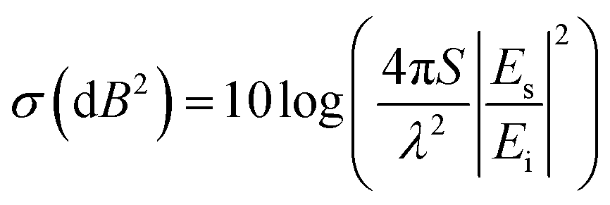
Using CST Studio Suite 2020 for the simulation of SiCN-5, SiCN-7 and SiCN-9 RCS, a rectangular model with dimensions of 200 mm in length and width was created. The model consists of a perfect electrical conductor (PEC) and an absorber coating with thicknesses of 1 mm and 3 mm, respectively. Placed on the YOZ plane, the model plate is subjected to incident electromagnetic waves from the positive X axis direction towards the negative X axis direction. Open boundary conditions were applied in all directions, while field monitoring frequency was set at 7.2 GHz. RCS can be defined as:11| |
 | (1) |
in the formula, Es is the electric field intensity of the scattered wave, S represents the area of the simulation model, λ is the wavelength of the electromagnetic wave, and Ei is the electric field intensity of the incident wave.
Results and discussion
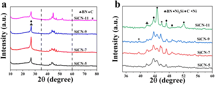
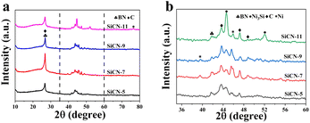
Fig. 1 shows the XRD results under different NA mass fractions. It can be seen from Fig. 1(a) that with the increase of NA content, the diffraction peaks of graphite carbon and nickel increased first and then decreased.12,13 The diffraction peak of graphite carbon of SiCN-7 was the strongest, indicating that the crystallinity of carbon in the sample was the highest. Fig. 1(b) is a map obtained by amplifying the range of 35–60°, which is used to observe the effect of adding NA more clearly. It can be seen that the diffraction peaks belonging to Ni3Si at 44.6° and 52.1° show a trend of decreasing first and then increasing.12 In addition, as the NA continues to increase, the diffraction peaks of Ni and Ni3Si show opposite trends, indicating that there is a certain phase transition between them.
 |
| | Fig. 1 XRD patterns of SiCN(Ni)/BN ceramics. | |
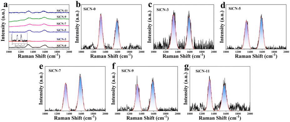
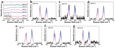
The effect of different mass fractions of NA on the carbon structure in the material was studied by Raman spectroscopy.14 The Raman spectra of the prepared SiCN(Ni)/BN ceramics were analyzed with Fig. 2 showing the D peak at 1350 cm−1 representing sample disorder while the G peak at 1580 cm−1 represents graphitization degree.15 In general, the value of ID/IG represents the degree of disorder or graphitization in the sample.16 The introduction of Ni has a great influence on the carbon structure of the sample. Then the Gaussian function Fourier transform is performed on the Raman curve, and the obtained data are shown in Table 3. It can be found that with the addition of NA, the value of ID/IG decreases first and then increases, and the graphitization degree of carbon increases first and then decreases.17 The value of ID/IG of SiCN-7 is the smallest, and the graphitization degree of carbon is higher, which is consistent with the results of XRD.
 |
| | Fig. 2 The Raman spectrum of SiCN(Ni)/BN ceramics. | |
Table 3 Gaussian fitting data
| Sample |
WD (cm−1) |
FD (cm−1) |
WG (cm−1) |
FG (cm−1) |
ID/IG |
| SiCN-0 |
1324.59 |
62.69 |
1595.41 |
62.36 |
1.41 |
| SiCN-3 |
1330.71 |
69.96 |
1588.29 |
62.03 |
1.19 |
| SiCN-5 |
1338.23 |
63.52 |
1588.14 |
64.99 |
0.86 |
| SiCN-7 |
1340.92 |
62.55 |
1586.53 |
69.84 |
0.72 |
| SiCN-9 |
1331.96 |
66.83 |
1586.68 |
68.49 |
0.85 |
| SiCN-11 |
1327.57 |
57.61 |
1572.29 |
79.07 |
0.91 |
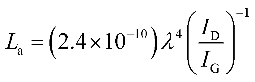
The plane crystallite sizes of graphite in the SiCN(Ni)/BN composites are calculated according to the Cancado formula (Formula (2)).18,19
| |
 | (2) |
Among them. La is the plane grain size of graphite, λ is the wavelength of the excitation light source. The excitation wavelength used in this experiment is 532 nm, ID and IG are the area of D peak and G peak respectively. The La size of the sample is shown in Table 4. Larger graphite size is beneficial to produce large polarization loss and conduction loss, thereby enhancing the material's ability to lose electromagnetic waves.
Table 4 The calculation results of SiCN (Ni)/BN composites based on Raman spectroscopy
| Samples |
SiCN-0 |
SiCN-3 |
SiCN-5 |
SiCN-7 |
SiCN-9 |
SiCN-11 |
| La (nm) |
13.63 |
16.15 |
22.35 |
26.70 |
22.62 |
21.13 |
| Nd (cm−2) |
4.22 × 10¹¹ |
3.57 × 10¹¹ |
2.58 × 10¹¹ |
2.16 × 10¹¹ |
2.55 × 10¹¹ |
2.73 × 10¹¹ |
The performance of absorbing electromagnetic waves is related to the defects of graphite, which may form a polarization center that dissipates electromagnetic wave energy. The defect density of graphite is calculated according to formula (3).20
| |
 | (3) |
ND is the point defect density of carbon. The ND value is inversely proportional to the La value. The lower the point defect density of the carbon in the sample, the higher the degree of graphitization of the carbon, indicating that the addition of a certain amount of NA is beneficial to increase the size of the nano-carbon phase, so that the material obtains a certain conductive network structure and improves the conduction loss of SiCN(Ni)/BN.
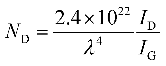
The effects of different mass fractions of NA on the chemical structure of the material were further explored by XPS spectroscopy. As shown in Fig. 3(a), the samples contained Si, B, C, O, Ni and other elements, further indicating that Ni was successfully doped into the SiCN ceramics. Fig. 3(b) is the high-resolution Si2p spectrum. It can be seen that there are four peaks, which belong to Si–N (101.8 eV), Si–C (103.37 eV) and Si–O (103.6 eV) bonds, respectively.21,22 There are three peaks in the high-resolution C1s of Fig. 3(c), which belong to C–Si (284.88 eV), C–C (285.55 eV) and C–O bond (289.31 eV), respectively.23 In Fig. 3(d) high-resolution N1s, 399.02, 398.45 eV and 400.78 eV are the peaks of N–B, N–Si and N–O bonds.24 The peaks of O1s are located at 530.54 eV, 533.49 eV and bond 532.89 eV, corresponding to O–N, O–C, O–Si bonds, respectively, as shown in Fig. 3(e). At the same time, Ni 2p3/2 and Ni 2p1/2 and their satellite peaks are shown in Fig. 3(f).25
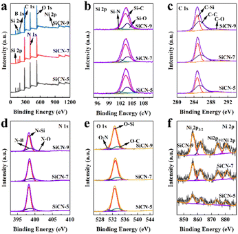 |
| | Fig. 3 The XPS spectrum of SiCN(Ni)/BN ceramics. | |
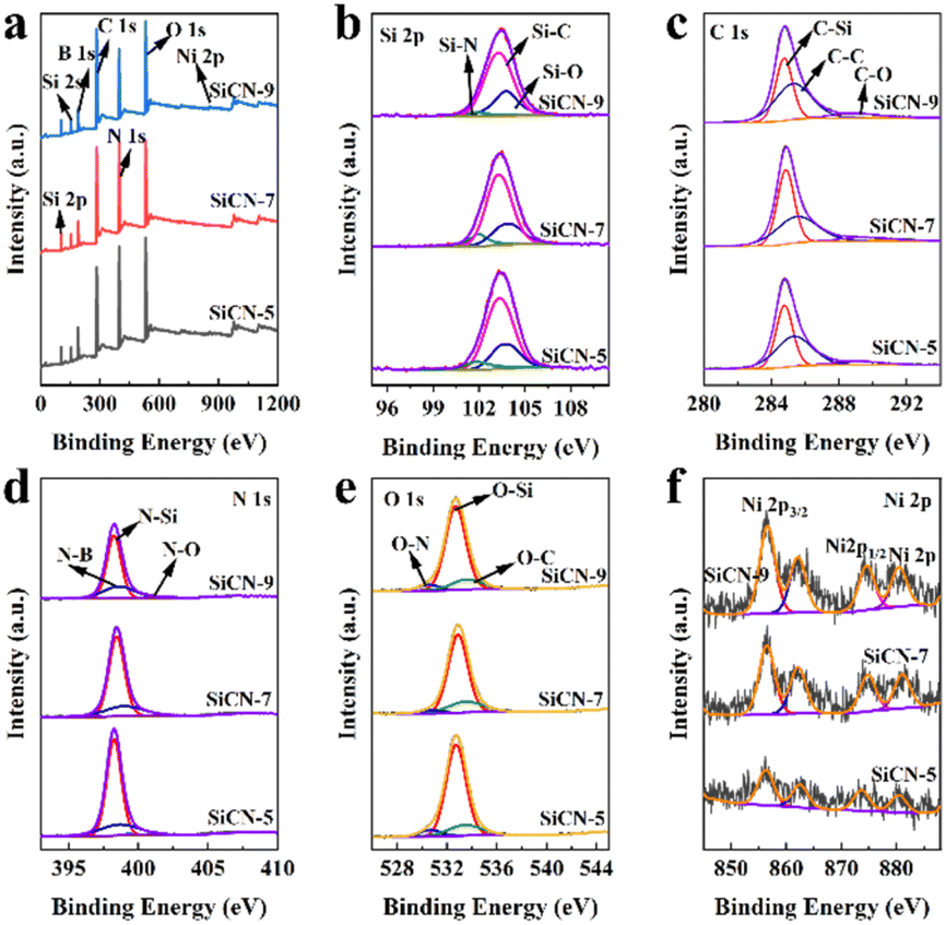
Fig. 4(a–e) show SEM images under different NA content conditions. From Fig. 4(a), it can be observed that the sheet structure belonging to BN has a smooth surface and no obvious pores. Fig. 4(b) and (c) show that with the increase of NA content, granular attachments appear and are evenly dispersed on the material surface and fracture site. In addition, with the further increase of NA content, the granular attachment disappeared, and a large number of nanowires appeared (Fig. 4(d)). The reason may be that in the process of high temperature pyrolysis, polysilazane is decomposed and cross-linked, releasing small gas molecules such as CH4 as carbon source, and in situ forming carbon nanowires under the catalysis of nickel.26–28 However, with further increased NA content, the nanowires disappeared and formed irregular clusters (Fig. 4(e)). EDS image of SiCN-7 (Fig. 4(f–m)) shows that all elements are evenly distributed. Among them, it can be seen from Fig. 4(k and m) that nickel is distributed more around the port, indicating that the particles attached in Fig. 4(b and c) may be Ni elemental. At the same time, the distribution of silicon around nickel indirectly proves the formation of Ni3Si.
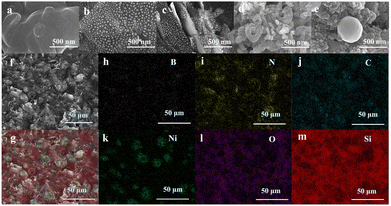 |
| | Fig. 4 The SEM pictures of (a) SiCN-0 (b) SiCN-3 (c) SiCN-7 (d) SiCN-9 (e) SiCN-11. The EDS images of SiCN-7 (f–m). | |
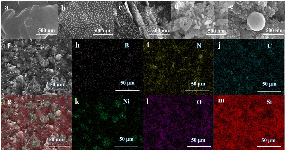
Fig. 5(a and b) is the transmission electron microscope image of SiCN-7. It can be seen from the figure that the granular attachment is Ni elemental and there is Ni3Si crystalline phase. TEM images of SiCN-9 powder showed the presence of a large number of nanowires (Fig. 5(c)). According to the high-resolution TEM image of Fig. 5(d), the lattice spacing of 0.2 nm corresponds to the (111) crystal plane of Ni3Si, while the lattice fringes belonging to elemental Ni disappear, which is consistent with the results of XRD and SEM.
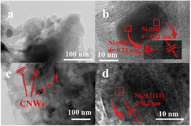 |
| | Fig. 5 The TEM pictures of (a) and (b) SiCN-7, (c) and (d) SiCN-9. | |
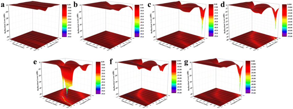
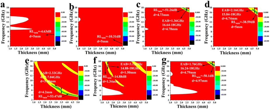
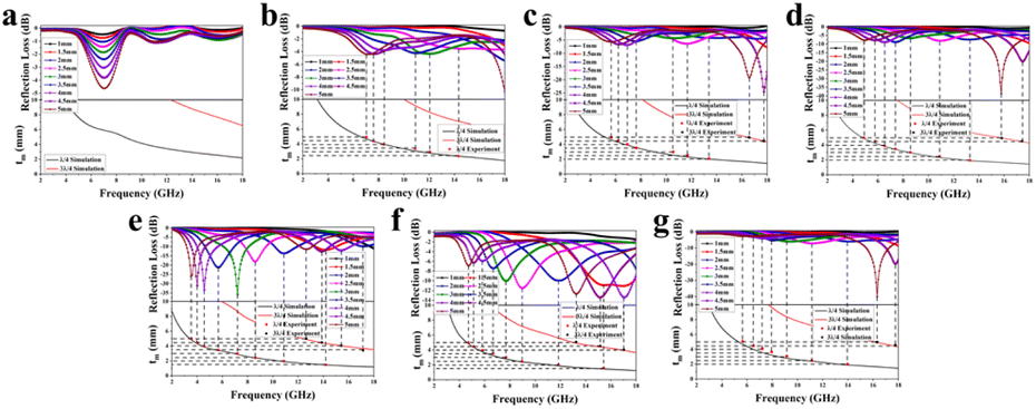
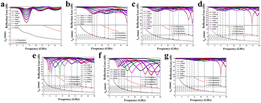
Fig. 6 and 7 are 3D plots and projections of the reflection loss for different NA mass fractions. One important parameter to measure materials' the absorption properties is reflection loss (RL).31 To observe its absorbing properties more intuitively we drew a 3D map of RL where RL values less than −10 dB indicate that over 90% of electromagnetic wave has been absorbed by the material. As shown in Fig. 7(a), SiCN-0 has the largest reflection loss and the worst absorption performance, and the reflection loss is only −4.63 dB when the thickness is 5 mm. With the addition of NA, the absorbing ability of the material is improved. SiCN-7 achieves the smallest reflection loss value of −53.47 dB at a thickness of 4.2 mm, and an EAB of 2.32 GHz at a thickness of 3.48 mm. The minimum return loss value of SiCN-9 is −14.88 dB (d = 1.34 mm), but the maximum effective bandwidth is 3.12 GHz at a thickness of 1.5 mm.
 |
| | Fig. 6 RLmin of (a) SiCN-0 (b) SiCN-1 (c) SiCN-3 (d) SiCN-5 (e) SiCN-7 (f) SiCN-9 (g) SiCN-11. | |
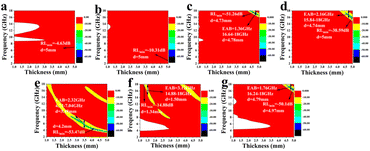 |
| | Fig. 7 RLmin projection of (a) SiCN-0 (b) SiCN-1 (c) SiCN-3 (d) SiCN-5 (e) SiCN-7 (f) SiCN-9 (g) SiCN-11. | |
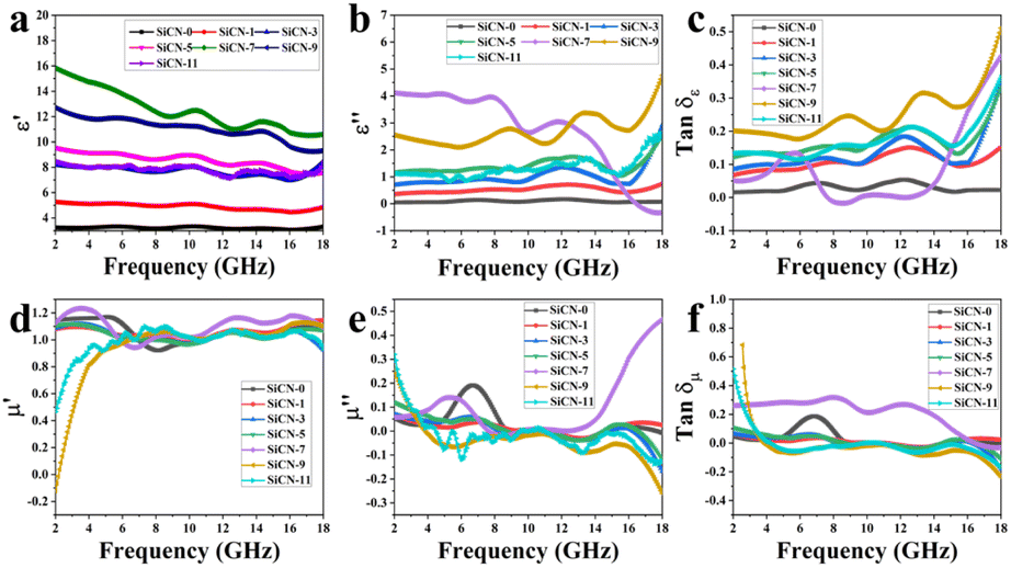
Dielectric constant (εr = ε′ − jε′′) and magnetic permeability (μr = μ′ − jμ′′) are also important factors to characterize the performance of absorbing materials.29 The real and imaginary parts of the dielectric constants of the samples are shown in Fig. 8(a and b). In the range of 2–18 GHz, the real and imaginary parts of the dielectric constant increase with the addition of NA and the increase of mass fraction, but after 12 GHz, the ε′′ of SiCN-7 gradually decreases and even appears negative, which may be caused by the electric polarization process does not follow the change of the external field. It is well known that the permeability of non-magnetic materials is close to 1 in the real part and 0 in the imaginary part. It can be observed from Fig. 8(d and e) that the permeability parameter of the material is low, pointing out that the magnetic loss contributes less to the electromagnetic wave absorption. Meanwhile, in Fig. 8(e), the magnetic loss generated by Ni and Ni3Si cannot offset the magnetic field generated inside the material, but radiates the magnetic energy to the external environment, so μ′′ is negative at higher frequencies. In general, dielectric loss and magnetic loss capacity are evaluated using tan![[thin space (1/6-em)]](https://www.rsc.org/images/entities/char_2009.gif) δε and tanδμ.30 As shown in Fig. 8(c and f), formant peaks appear in images tanδε and tanδμ due to resonance phenomenon. Although SiCN-7 has better electromagnetic wave absorption performance, SiCN-9 has better dielectric properties, which may be due to the formation of more conductive phases such as CNWs in SiCN-9. Relatively speaking, SiCN-7 has a higher tan value, indicating that the material has better magnetic loss ability.
δε and tanδμ.30 As shown in Fig. 8(c and f), formant peaks appear in images tanδε and tanδμ due to resonance phenomenon. Although SiCN-7 has better electromagnetic wave absorption performance, SiCN-9 has better dielectric properties, which may be due to the formation of more conductive phases such as CNWs in SiCN-9. Relatively speaking, SiCN-7 has a higher tan value, indicating that the material has better magnetic loss ability.
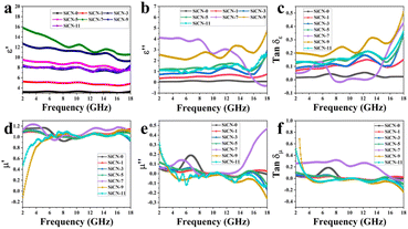 |
| | Fig. 8 (a) ε′ (b) ε′′ (c) tanδε (d) μ′ (e) μ′′ (f) tanδμ of SiCN(Ni)/BN ceramics. | |
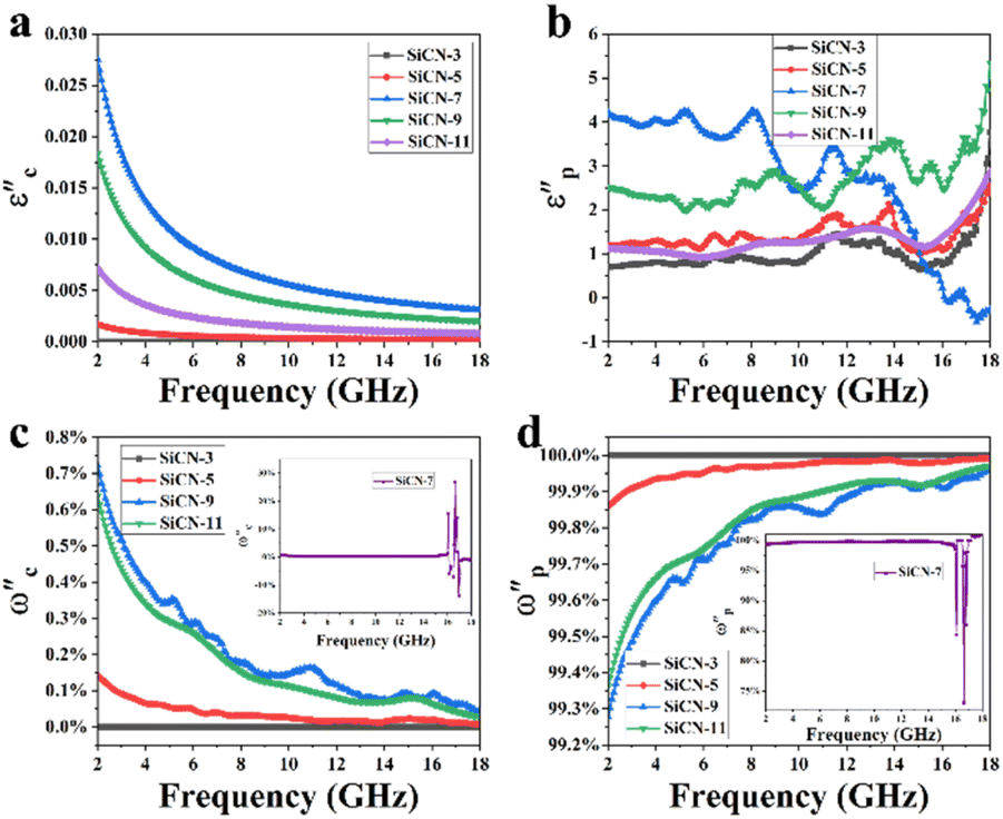
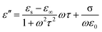
ε′ and ε′′ reflect the storage and consumption of electromagnetic energy, and further study of the electromagnetic energy absorption mechanism can reveal the profound significance of the electromagnetic energy absorption mechanism. Debye theory believes that due to the difference between the polarization time and the period of the external electromagnetic field, the polarization process of the dipole lags behind the change of the external electromagnetic field, resulting in the loss of electromagnetic energy. The imaginary part (ε′′) of the dielectric constant consists of two parts, the polarization loss (ε′′p) and the conduction loss (ε′′c). The conduction loss is related to the material's electrical conductivity, and the electrical conductivity calculated according to Ohm's law is shown in Table 5. Due to the low conductivity of SiCN-3, the conduction loss of the sample can be neglected. It can be seen from Fig. 9(a and b) that after adding NA, the values of ε′′p and ε′′c increase significantly, indicating that the addition of NA increases the dielectric loss of the material, and the conduction loss dominates.32,33 The ratio of polarization loss to total energy attenuation can be expressed as ω′c = ε′′c/(ε′′c + ε′′p). The ratio of conduction loss to total energy attenuation can be expressed as ω′p = ε′′p/(ε′′c + ε′′p). As shown in Fig. 9(c and d), the polarization loss accounts for more than 99% in the frequency range of 2–18 GHz.34
Table 5 The conductivity of SiCN(Ni)/BN ceramics
| Samples |
SiCN-3 |
SiCN-5 |
SiCN-7 |
SiCN-9 |
SiCN-11 |
| σ (s cm−1) |
9.74 × 10⁻¹⁰ |
1.88 × 10⁻⁴ |
3.06 × 10⁻³ |
2.04 × 10⁻³ |
7.99 × 10⁻⁴ |
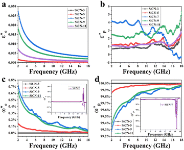 |
| | Fig. 9 The (a) ε′′c, (b) ε′′p, (c) ω′′c and (b) ω′′p of SiCN(Ni)/BN ceramics. | |
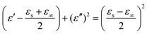
The Cole–Cole semicircle is widely used to analyze the polarization relaxation process. According to Debye theory, ε′ and ε′ conform to the following formula:
| |
 | (4) |
| |
 | (5) |
| |
 | (6) |
where
ε∞ and
εs represent the permittivity and electrostatic permittivity of infinite frequency, respectively.
ω is the angular frequency,
ε0, σ,
τ are the dielectric constant, conductivity and polarization relaxation time in vacuum, respectively. The
ε′ and
ε′′ curves should consist of semi-circles, where each semi-circle implies a typical Debye relaxation process. As can be seen from
Fig. 10, more than one
ε′ −
ε′′ semicircle exists in all the synthesized samples, indicating the existence of multiple polarization relaxation phenomena in the samples. Further observation shows that there is a flat area at the tail of the
ε′ −
ε′′ semicircle of the sample, indicating that there is a certain transfer loss in the material, which may be caused by the crystalline carbon and other substances generated during the sintering process of the sample to increase the conductivity of the sample.
35
 |
| | Fig. 10 The Cole–Cole curves of SiCN(Ni)/BN ceramics. | |
Another mechanism that contributes to the loss of absorbing materials is interference. In general, there exists a correlation referred to as the quarter wavelength theory between the absorption peak frequency of electromagnetic waves and the thickness of the absorbing layer. It can be expressed by the following formula:36
| |
 | (7) |
in the formula:
fm is the absorption peak frequency,
tm is the corresponding absorption layer thickness. From
eqn (7), when the thickness of the absorbing material is a quarter wavelength of the EMW, the incident EMW and the reflected EMW interfere at the interface.
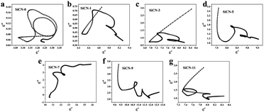
Fig. 11 indicates that the RL
min peaks obtained by the SiCN-3, SiCN-5, SiCN-7, SiCN-9 and SiCN-11 samples in the experiment basically fall on the matching thickness curve calculated by the
λ/4 model. This implies that it is possible to derive a corresponding matching thickness for a given material's RL
min value, which would be highly beneficial for actual material preparation.
 |
| | Fig. 11 Equal thickness matching curve of (a) SiCN-0 (b) SiCN-1 (c) SiCN-3 (d) SiCN-5(e) SiCN-7 (f) SiCN-9 (g) SiCN-11. | |
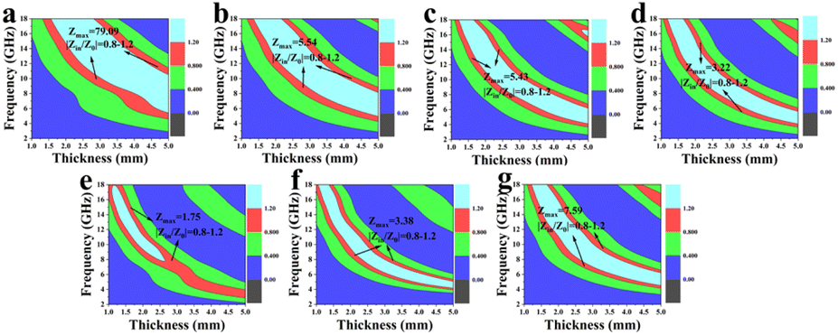
Fig. 12 displays impedance matching under different NA content conditions. Impedance matching plays a crucial role in determining material absorption performance.37 Generally speaking, when a material's impedance matches closer to 1, electromagnetic waves can enter and be absorbed more easily by the material resulting in better absorbing performance. The optimal impedance matching range (OIM) is between 0.8 and 1.2. The Zmax of SiCN-0 is 79.09, which differs significantly from the optimal impedance matching value. With the addition of NA, the impedance matching value gradually decreases, indicating that the addition of NA can effectively adjust the impedance matching of the material, which may be due to the joint action of the generated Ni, Ni3Si and crystalline carbon to improve the dielectric loss and magnetic loss of the material, so as to effectively adjust the impedance matching of the material. The maximum impedance matching value of SiCN-7 is 1.75, and the best impedance matching value range is the largest, and the impedance matching performance is the best, which is conducive to more electromagnetic waves entering the material, thereby improving the electromagnetic wave absorption performance of the material.
 |
| | Fig. 12 The plots of |Zin/Z0| with thickness from 1–5 mm of (a) SiCN-0 (b) SiCN-1 (c) SiCN-3 (d) SiCN-5 (e) SiCN-7 (f) SiCN-9 (g) SiCN-11. | |
In order to achieve zero reflection, the impedance of the absorber should be close to the air space. A delta function has been suggested as a means of assessing impedance matching:
| | |
|Δ| = |sinh2(Kfd) − M|
| (8) |
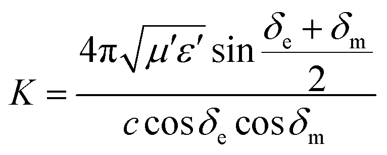
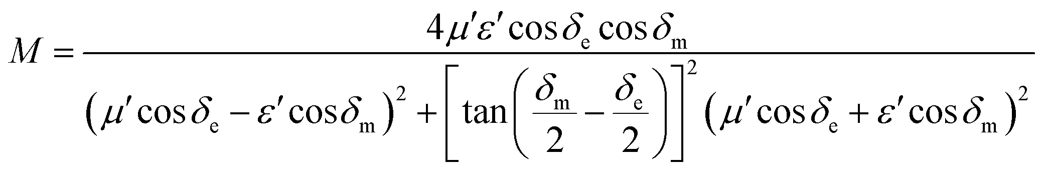
K and M are determined from the electromagnetic parameters by the following equations:
| |
 | (9) |
| |
 | (10) |
where
δm = arctan(
μ′′/
μ′) and
δe = arctan(
ε′′/ε′) are the magnetic loss angle and the dielectric loss angle, respectively.
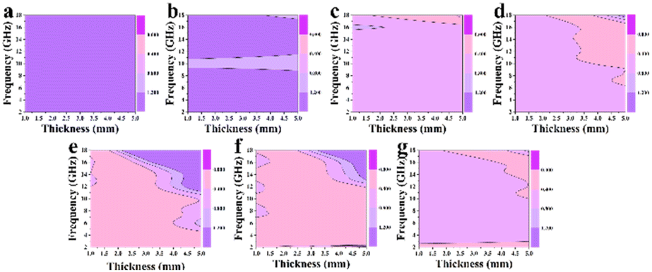
38 A 2D plot of the delta value of the sample calculated from the delta function and the measured electromagnetic parameters is shown in
Fig. 13. It can be observed from
Fig. 13(c, d) and (g) that the pink-purple regions (close to 0) of SiCN-3, SiCN-5 and SiCN-11 appear in the high frequency range, which is consistent with the absorption behavior of electromagnetic waves described above. The area of pink and purple region of SiCN-7 (
Fig. 13(e)) and SiCN-9 (
Fig. 13(f)) samples is significantly larger than that of other component samples, indicating that Ni, Ni
3Si and crystalline carbon generated after adding NA can improve the impedance matching performance of the material.
 |
| | Fig. 13 Impedance matching degree delta of (a) SiCN-0 (b) SiCN-1(c) SiCN-3 (d) SiCN-5 (e) SiCN-7 (f) SiCN-9 (g) SiCN-11. | |
The natural resonance, eddy current loss and domain wall resonance of electromagnetic wave absorbing materials are all magnetic losses. The influence of eddy current resonance and natural resonance on the magnetic loss of SiCN(Ni)/BN ceramics can be reflected by the value of C0, the formula is as follows:39,40
Fig. 14 is the C0 diagram of SiCN (Ni)/BN ceramics. Generally, when magnetic loss is overshadowed by eddy current loss, the frequency does not affect the value of C0. The findings indicate that within the 2–18 GHz frequency range, eddy current loss accounts for a minor portion while natural resonance loss predominantly contributes to the magnetic loss observed in the sample.
 |
| | Fig. 14 The C0 curves of SiCN(Ni)/BN ceramics. | |
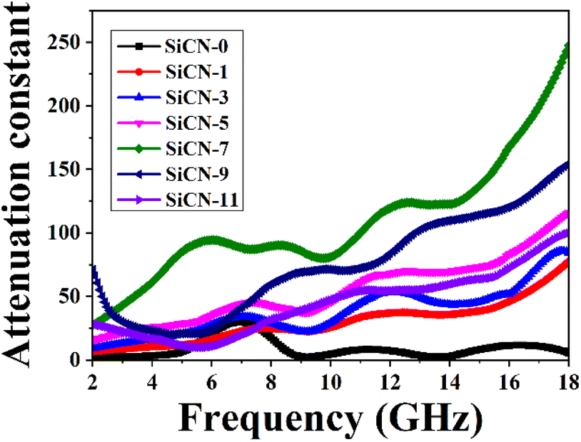
Another parameter that characterizes the absorbing properties of absorbing materials is the attenuation constant, which indicates the attenuation of electromagnetic waves inside the absorbing materials.41 Fig. 15 shows the attenuation constants under different NA content conditions. With the addition of NA, the attenuation constant of the sample increases. This may be because the addition of NA provides a certain magnetic loss for the material, and the attenuation capacity of the material depends largely on the effective complementarity of dielectric loss and magnetic loss. SiCN-7 has the largest attenuation constant and the best impedance matching performance, and more electromagnetic waves are attenuated and lost after entering the material, so that the material has the best electromagnetic wave absorption performance.
 |
| | Fig. 15 The attenuation constants of SiCN(Ni)/BN ceramics. | |
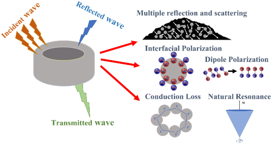
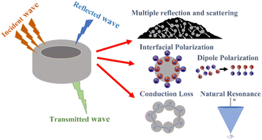
Fig. 16 illustrates the absorbing mechanism of SiCN(Ni)/BN ceramics, providing further insight into its absorption properties. The material contains amorphous carbon, Ni, CNWs, and Ni3Si particles that contribute to its excellent dielectric losses through interface polarization, dipole orientation polarization, and conduction losses. Additionally, natural resonance losses and multiple reflections of electromagnetic waves enhance its magnetic losses. The presence of in situ generated Ni3Si and CNWs creates numerous heterointerfaces and polarization sites that boost interface polarization and dipole orientation polarization while also increasing conductivity by forming a conductive network. Furthermore, the inclusion of Ni metal imparts magnetic properties to the material primarily through natural resonance. These various absorption mechanisms work together synergistically to give SiCN(Ni)/BN ceramics exceptional EMW absorption capabilities.
 |
| | Fig. 16 The absorption mechanism of SiCN(Ni)/BN ceramics. | |
Compared with the wave-absorbing properties of polymer-converted ceramics reported in other literature, the results are shown in Table 6. The SiCN(Ni)/BN ceramics synthesized in this paper have excellent EMW absorbing properties. The optimal RLmin and EAB of SiCN(Ni)/BN ceramics are −53.47 dB (4.2 mm) and 3.12 GHz (14.88–18 GHz, 1.50 mm), respectively.
Table 6 Absorption performance compared to references
| Materials |
RLmin (dB) |
EAB (GHz) |
d (mm) |
T (°C) |
Ref. |
| SiCN |
−31.10 |
4.59 |
2 |
1300 |
29 |
| SiOC |
−23.50 |
4.9 |
1.58 |
1200 |
13 |
| SiBCN |
−54.91 |
4.72 |
1.75 |
1300 |
15 |
| SiCN(Fe) |
−47.64 |
4.28 |
1.38 |
1100 |
21 |
| SiCN |
−53.10 |
5.6 |
1.95 |
1300 |
23 |
| SiCN(Ni) |
−53.47 |
3.12 |
1.50 |
1100 |
This work |
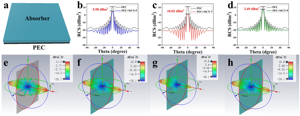
Fig. 17 shows the CST simulation results of a perfect conductor and SiCN-7 coated sample, showing the electromagnetic wave absorption characteristics of the material at different angles under far-field conditions. Fig. 17(a) is a schematic diagram of the model used in the simulation, which consists of a bottom PEC plate and an upper absorber. The simulation results of one-dimensional RCS are shown in Fig. 17(b–d). At 7.2 GHz, the microwave scattering signals of PEC + SiCN-5, PEC + SiCN-7 and PEC + SiCN-9 are all smaller than those of PEC plates, and the RCS value of SiCN-7 is lower and the coverage Angle is larger, indicating that SiCN-7 coating can effectively inhibit the reflection and scattering of electromagnetic waves on PEC surfaces. Fig. 17(e–h) shows the 3D radar scattered signals of PEC, PEC + SiCN-5, PEC + SiCN-7 and PEC + SiCN-9, respectively. After the coating of the material, the radar scattering signal is weakened, which indicates that the material has a certain attenuation effect on the electromagnetic wave on the PEC surface, and further indicates that SiCN(Ni)/BN has practical application potential in the field of electromagnetic wave absorption.
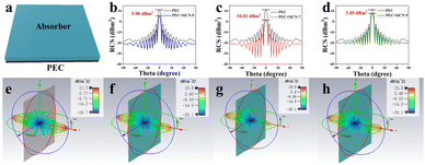 |
| | Fig. 17 Schematic diagram of RCS simulation (a). RCS simulation curves (b) SiCN-5, (c) SiCN-7, (d) SiCN-9. CST simulation diagram (e) PEC, (f) PEC + SiCN-5, (g) PEC + SiCN-7, (h) SiCN-9. | |
Conclusions
The SiCN(Ni)/BN ceramics prepared in this paper possess low density, high thermal stability and good electromagnetic properties, which are of great significance for promoting the development of EMW absorbing materials. Through the analysis of electrical conductivity, it is found that the proportion of polarization loss in dielectric loss reaches more than 99%; the introduction of nickel acetylacetonate catalyzes the formation of CNWs, and in situ formation of Ni and Ni3Si, which effectively improves the impedance matching of ceramic powders performance. The EMW absorbing performance of SiCN(Ni)/BN ceramics show a trend of first increasing and then decreasing with the increase of nickel acetylacetonate content. When the content of NA reaches 7 wt%, the optimal impedance matching range increases, and the RLmin can reach −53.47 dB at 4.2 mm. The RCS value of SiCN-7 is less than −10 dBm2 in the near −90–90 range, which provide a theoretical basis for the application of SiCN(Ni)/BN ceramics.
Author contributions
Yanchun Tong: Investigation, software, formal analysis, data curation, writing - original draft. Chunmiao Liu: Investigation, data curation, writing - review & editing. Chang Liu: Data curation, validation, formal analysis. Haibin Sun: Resources, funding acquisition. Hui Peng: Formal analysis. Qiangqiang Hu: Resources, funding acquisition. Shigang Wu: Investigation, supervision. Yujun Zhao: Investigation, supervision. Xue Guo: Methodology, conceptualization, investigation, writing - review & editing, resources, funding acquisition. Yurun Feng: Methodology, conceptualization, investigation, supervision.
Conflicts of interest
There are no conflicts to declare.
Acknowledgements
This work was supported by National Natural Science Foundation of China (52302100), Natural Science Foundation of Shandong Province (ZR2023ME140, ZR2022QE024), Zibo Key Research and Development Project (2021SNPT0004) and Fundamental Science on Nuclear Wastes and Environmental Safety Laboratory (20kfhk02).
Notes and references
- Y. Liu, Preparation and Absorbing Properties of PDCs-SiCN Ceramics Containing Magnetic Particles. Shandong University, 2019 Search PubMed.
- X. G. Chen, Y. Ye and J. P. Cheng, Recent Progress in Electromagnetic Wave Absorbers, J. Inorg. Mater., 2011, 26(5), 449–457 CrossRef CAS.
- J. Zhang, W. Y. Zhang and Z. P. Xi, Research progress of stealth absorbing materials, Rare Met. Mater. Eng., 2008, 37(S4), 504–508 Search PubMed.
- J. Wang, Y. F. Shi, C. Yang and F. Feng, A review and prospects of operational frequency selecting techniques for HF radio communication, Adv. Space Res., 2022, 69(8), 2989–2999 CrossRef.
- Y. H. Zhang, H. X. Si, S. C. Liu, Z. Y. Jiang, J. W. Zhang and C. H. Gong, Facile synthesis of BN/Ni nanocomposites for effective regulation of microwave absorption performance, J. Alloys Compd., 2021, 850, 156680 CrossRef CAS.
- C. M. Huang, Application Research and Development Prospects of Porous Materials, Equipment Manufacturing Technology, 2014,(02), 230–232 CrossRef CAS.
- W. Zhou, L. Long, P. Xiao, C. K. Jia and Y. Li, Comparison in dielectric and microwave absorption properties of SiC coated carbon fibers with PyC and BN interphases, Surf. Coat. Technol., 2019, 359, 272–277 CrossRef CAS.
- V. Cekdar, S. Tugce, G. Aleksander and S. Domenico, Polymer derived ceramic aerogels, Curr. Opin. Solid State Mater. Sci., 2021, 25(4), 100936 CrossRef.
- J. J. Li, F. Zhang, H. B. Lu, W. B. Guo, X. D. He and Y. Yuan, Heterogeneous rod-like Ni@C composites toward strong and stable microwave absorption performance, Carbon, 2021, 181(30), 358–369 CrossRef CAS.
- L. Aljerf and R. Nadra, Developed greener method based on MW implementation in manufacturing CNFs, Int. J. Nanomanuf., 2019, 15(3), 100461 Search PubMed.
- Z. Zhe, M. Q. Ning, Z. K. Lei, X. H. Zhuang, G. G. Tan, J. H. Hou, H. Xu, Q. K. Man, J. B. Li and R. W. Li, 0D/1D/2D architectural Co@C/MXene composite for boosting microwave attenuation performance in 2-18 GHz, Carbon, 2022, 193(30), 182–194 Search PubMed.
- C. J. Cui, J. Zhang, K. Wu, D. N. Zou, Y. P. Ma, L. Liu and H. Z. Fu, Directional solidification of Ni–Ni3Si eutectic in situ composites by electron beam floating zone melting, Phys. B, 2013, 412(1), 70–73 CrossRef CAS.
- Y. R. Feng, X. Guo, K. Huang, H. Elsayed, G. Franchin, H. Y. Gong and C. Paolo, Enhanced electromagnetic microwave absorption of SiOC ceramics targeting the integration of structure and function, J. Eur. Ceram. Soc., 2021, 41(13), 6393–6405 CrossRef CAS.
- A. V. Stanishevsky, L. Y. Khriachtchev and R. Lappalainen, On correlation between the shape of Raman spectra and short-range order structure of hydrogenfree amorphous carbon flms, Diamond Relat. Mater., 1997, 6(8), 1026–1030 CrossRef CAS.
- J. Liu, Y. R. Feng, C. M. Liu, Y. C. Tong, H. B. Sun, H. Peng, S. G. Wu, J. B. Lu, H. Y. Gong, X. Guo and J. Li, Novel SiBCN composite fibers with broadband and strong electromagnetic wave absorption performance, J. Alloys Compd., 2022, 912(15), 165190 CrossRef CAS.
- G. Mera, R. Riedel, F. Poli and K. Müller, Carbon-rich SiCN ceramics derived from phenyl-containing poly (silylcarbodiim ides), J. Eur. Ceram. Soc., 2009, 29(13), 2873–2883 CrossRef CAS.
- G. Gökçeli, S. Bozoğlu and N. Karatepe, Cobalt-molybdenum bimetallic catalyst effect on biomass-derived graphitic carbon, J. Anal. Appl. Pyrolysis, 2023, 174, 106152 CrossRef.
- Y. Bleu, F. Bourquard, A. S. Loir, V. Barnier, F. Garrelie and C. Donnet, Raman study of the substrate influence on graphene synthesis using a solid carbon source via rapid thermal annealing, J. Raman Spectrosc., 2019, 50(11), 1630–1641 CrossRef CAS.
- P. Saini, R. Sharma and N. Chadha, Determination of defect density, crystallite size and number of graphene layers in graphene analogues using X-ray diffraction and Raman spectroscopy, Indian J. Pure Appl. Phys., 2017, 55(9), 625–629 Search PubMed.
- P. G. Chen, J. X. Chen, C. G. Wang, X. C. Li, Y. L. Zhu and B. Q. Zhu, The heterointerface of graphene in-situ growth for enhanced microwave attenuation properties in La-doped SiBCN ceramics, Ceram. Int., 2023, 49(16), 26642–26653 CrossRef CAS.
- Y. Feng, X. Guo and J. Lu, Enhanced electromagnetic wave absorption performance of SiCN(Fe) fbers by in-situ generated Fe3Si and CNTs, Ceram. Int., 2021, 47(14), 19582–19594 CrossRef CAS.
- Y. Cao, L. Nyborg and U. Jelvestam, XPS calibration study of thin-flm nickel silicides, Surf. Interface Anal., 2009, 41(6), 471–483 CrossRef CAS.
- P. Wang, L. Cheng and L. Zhang, Lightweight, flexible SiCN ceramic nanowires applied as effective microwave absorbers in high frequency, Chem. Eng. J., 2018, 338(15), 248–260 CrossRef CAS.
- Z. W. Gao, F. Ye, L. F. Cheng, K. Zhao, R. H. Liu and S. W. Fan, A novel strategy to prepare BN interface and its effects on microstructure and properties of SiCw/BN/SiC composites, J. Alloys Compd., 2021, 858(25), 158218 CrossRef CAS.
- T. Xia, Y. Wang and C. Mai, et al., Facile in situ growth of ZnO nanosheets standing on Ni foam as binder-free anodes for lithium-ion batteries, RSC Adv., 2019, 9(34), 19253–19260 RSC.
- J. B. Lu, Y. R. Feng, J. Liu, C. M. Liu, Y. C. Tong, S. G. Wu, H. B. Sun, H. Y. Gong and X. Guo, Improved electromagnetic wave absorbing performance of PDCs-SiCN(Ni) fibers with different nickel content, Ceram. Int., 2022, 48(16), 23578–23589 CrossRef CAS.
- F. Guo, Z. Liu, Y. Y. Zhang, J. Xiao, X. Y. Zeng, C. X. Zhang, P. Dong, T. T. Liu, Y. J. Zhang and M. Li, Tiny Ni nanoparticles embedded in boron- and nitrogen-codoped porous carbon nanowires for high-efficiency water splitting, ACS Appl. Mater. Interfaces, 2022, 14(21), 24447–24461 CrossRef CAS PubMed.
- X. M. Liu, M. H. Li, H. Q. Liu, W. Y. Duan, C. Fasel, Y. C. Chen, F. M. Qu, W. J. Xie, X. M. Fan, R. Riedel and A. Weidenkaff, Nanocellulose-polysilazane single-source-precursor derived defect-rich carbon nanofibers/SiCN nanocomposites with excellent electromagnetic absorption performance, Carbon, 2022, 188, 349–359 CrossRef CAS.
- F. Xiao, H. Sun, J. Li, X. Guo, H. Zhang, J. B. Lu, Z. X. Pan and J. K. Xu, Electrospinning preparation and electromagnetic wave absorption properties of SiCN fbers, Ceram. Int., 2020, 46(8), 12773–12781 CrossRef CAS.
- Y. Liu, Y. Feng, H. Gong, Y. J. Zhang, X. Lin, B. Y. Xie and J. J. Mao, Microwave absorbing performance of polymerderived SiCN(Ni) ceramics prepared from different nickel sources, J. Alloys Compd., 2018, 749(15), 620–627 CrossRef CAS.
- X. Jian, B. Wu, Y. Wei, S. X. Dou, X. L. Wang, W. D. He and N. Mahmood, Facile synthesis of Fe3O4/GCs composites and their enhanced microwave absorption properties, ACS Appl. Mater. Interfaces, 2016, 8(9), 6101–6109 CrossRef CAS PubMed.
- F. Cao, F. Yan, J. Xu, C. H. Zhu, L. H. Qi, C. Y. Li and Y. J. Chen, Tailing size and impedance matching characteristic of nitrogen-doped carbon nanotubes for electromagnetic wave absorption, Carbon, 2021, 174(15), 79–89 CrossRef CAS.
- Y. Rao, X. Qi, Q. Peng, Y. L. Chen, X. Gong, R. Xie and W. Zhong, Mixed-dimensional conductive network heterostructures: An effective interfacial strategy to aggrandize dielectric loss for designing microwave absorbers, J. Alloys Compd., 2022, 910(25), 164974 CrossRef CAS.
- F. Chen, S. Zhang, B. B. Ma, Y. Xiong, H. Luo, Y. Z. Cheng, X. C. Li, X. Wang and R. Z. Gong, Bimetallic CoFe-MOF@ Ti3C2Tx MXene derived composites for broadband microwave absorption, Chem. Eng. J., 2022, 431(1), 134007 CrossRef CAS.
- S. Cheng, C. Zhang, H. Wang, J. R. Ye, Y. Li, Q. Zhuang, W. Dong and A. M. Xie, Carbon nanofilm stabilized twisty V2O3 nanorods with enhanced multiple polarization behavior for electromagnetic wave absorption application, J. Mater. Sci. Technol, 2022, 119(20), 37–44 CrossRef CAS.
- X. Y. Zhang, Z. R. Jia, F. Zhang, Z. H. Xia, J. X. Zou, Z. Gu and G. L. Wu, MOF-derived NiFe2S4/porous carbon composites as electromagnetic wave absorber, J. Colloid Interface Sci., 2022, 610(15), 610–620 CrossRef CAS PubMed.
- N. Li, G. W. Huang and Y. Q. Li, Enhanced microwave absorption performance of coated carbon nanotubes by optimizing the Fe3O4 nanocoating structure, ACS Appl. Mater., 2017, 9(3), 2973–2983 CrossRef CAS PubMed.
- F. Chen, S. Zhang, R. Guo, Y. Xiong, H. Luo, Y. Z. Cheng, X. C. Li, X. Wang and R. Z. Gong, 1D magnetic nitrogen doped carbon-based fibers derived from NiFe Prussian blue analogues embedded polyacrylonitrile via electrospinning with tunable microwave absorption, Composites, Part B, 2021, 224(1), 109161 CrossRef CAS.
- W. D. Zhang, Y. Zheng, X. Zhang, Q. Zhu, H. X. Yan, L. F. Liotta and H. J. Qi, Synthesis and mechanism investigation of wide-bandwidth Ni@MnO2 NS foam microwave absorbent, J. Alloys Compd., 2019, 792(5), 945–952 CrossRef CAS.
- X. Meng, W. Lei, W. Yang, Y. Q. Liu and Y. S. Yu, Fe3O4 nanoparticles coated with ultra-thin carbon layer for polarization-controlled microwave absorption performance, J. Colloid Interface Sci., 2021, 600(15), 382–389 CrossRef CAS PubMed.
- J. Gao, Z. Ma, F. Liu and C. X. Chen, Synthesis of carbon-coated cobalt ferrite core-shell structure composite: A method for enhancing electromagnetic wave absorption properties by adjusting impedance matching, Chin. J. Chem. Eng., 2021, 47, 206–217 CrossRef.
|
| This journal is © The Royal Society of Chemistry 2024 |
Click here to see how this site uses Cookies. View our privacy policy here. 
 Open Access Article
 This Open Access Article is licensed under a Creative Commons Attribution-Non Commercial 3.0 Unported Licence
 *a and
Shigang Wu*a
*a and
Shigang Wu*a