
 Open Access Article
 This Open Access Article is licensed under a Creative Commons Attribution-Non Commercial 3.0 Unported Licence
High-sensitivity hybrid MoSe2/AgInGaS quantum dot heterojunction photodetector†
Xunjia Zhao‡
a,
Xusheng Wang‡ a,
Runmeng Jiaa,
Yuhai Lina,
TingTing Guoa,
Linxiang Wua,
Xudong Hua,
Tong Zhaoa,
Danni Yana,
Lin zhub,
Zhanyang Chenb,
Xinsen Xub,
Xiang Chen*a and
Xiufeng Song*a
a,
Runmeng Jiaa,
Yuhai Lina,
TingTing Guoa,
Linxiang Wua,
Xudong Hua,
Tong Zhaoa,
Danni Yana,
Lin zhub,
Zhanyang Chenb,
Xinsen Xub,
Xiang Chen*a and
Xiufeng Song*a
aMIIT Key Laboratory of Advanced Display Materials and Devices, School of Materials Science and Engineering, Nanjing University of Science and Technology, Nanjing 210094, China. E-mail: xiangchen@njust.edu.cn; xiufengsoong@njust.edu.cn
bShangdong Gemei Tungsten & Molybdenum Material Co. Ltd, Weihai 265222, China
First published on 9th January 2024
Abstract
Zero-dimensional (0D)–two-dimensional (2D) hybrid photodetectors have received widespread attention due to their outstanding photoelectric performances. However, these devices with high performances mainly employ quantum dots that contain toxic elements as sensitizing layers, which restricts their practical applications. In this work, we used eco-friendly AgInGaS quantum dots (AIGS-QDs) as a highly light-absorbing layer and molybdenum diselenide (MoSe2) as a charge transfer layer to construct a 0D–2D hybrid photodetector. Notably, we observed that MoSe2 strongly quenches the photoluminescence (PL) of AIGS-QDs and decreases the decay time of PL in the MoSe2/AIGS-QDs heterojunction. The MoSe2/AIGS-QDs hybrid photodetector demonstrates a responsivity of 14.3 A W−1 and a high detectivity of 6.4 × 10¹¹ Jones. Moreover, the detectivity of the hybrid phototransistor is significantly enhanced by more than three times compared with that of the MoSe2 photodetector. Our work suggests that 0D–2D hybrid photodetectors with multiplex I-III-VI QDs provide promising potential for future high-sensitivity photodetectors.
1. Introduction
In recent decades, graphene, being a representative 2D material, has gained significant attention due to its exceptionally high carrier mobility (2 × 105 cm2 V−1 s−1), wide range of optical absorption coefficients (7 × 105 cm−1), and excellent photoelectric conversion efficiency.1–3 These properties make it highly attractive for the development of high-speed and broadband photodetectors.4,5 Nonetheless, the semi-metallic property with low light absorptivity of only 2.3% results in the large dark current and low photoelectric response of graphene-based devices.6 This problem restricts the practical application of graphene in the field of photodetectors.7Hence, it is necessary to explore a new technology strategy with high light absorptivity to address this limitation. A commonly employed approach to enhance device performance is to integrate graphene with a high light absorption QDs.8 QDs have some exceptional properties with high light absorption coefficient, a wide range of adjustable bandgap, and a narrow linewidth in emission.9–11 Therefore, QDs have attracted extensive attention and applied in various fields such as photodetectors, solar cells, and LEDs. Konstantatos et al. demonstrated a hybrid graphene–quantum dot phototransistor with a gain of ∼108 electrons per photon and a responsivity of ∼107 A W−1.12,13 Hu et al. reported a graphene/InAs QDs/GaAs photodetector that has a responsivity of about 17.0 mA W−1 and detectivity of 2.3 × 10¹⁰ Jones.14 Zheng et al. revealed that the photoconductive gain and detectivity of graphene-perovskite quantum dot photodetector arrive at 3.7 × 10⁴ and 6 × 10⁷ Jones.15
Besides, the zero-band gap of graphene leads to the ultra-fast carrier recombination speed and ultra-short carrier lifetime.16 The graphene photodetectors do not satisfy the requirements of high-response optoelectronic devices due to the large dark current.17 Hence, two-dimensional transition metal dichalcogenide (2D TMDC) semiconductors exhibit appealing properties, such as tunable bandgaps, high electron mobility, flexibility, and the absence of dangling bonds on their surfaces.18–23 These characteristics enable 2D TMDCs to be an excellent candidate for the high-performance photodetector.24–26 In recent years, numerous 0D/2D heterostructures with outstanding properties have been explored and reported. For instance, Zhang et al. explored that the detectivity of MoS2/ZnCdSe heterostructure is reached to be 1.0 × 10¹² Jones.27 Hu et al. reported that the responsivity and detectivity of WSe2/PbS-QDs heterostructure are 2 × 10⁵ A W−1 and 1013 Jones, respectively.28 Mukherjee et al. found that the detectivity of MoS2/PbS-QDs heterostructure reaches up to 1012 Jones.29 Among these, PbS-QDs,30 HgTe-QDs,31 and CdS-QDs32 are commonly employed in the development of high-performance photodetectors. However, these devices face a challenge due to the presence of high-toxicity elements which limit their practical application.4 Hence, it is essential to explore alternative eco-friendly QDs possessing comparable characteristics in the photodetectors. So, low-toxicity QDs with a wide emission spectrum, tunable bandgap energy ranging from visible to near-infrared, and large Stokes shifts have emerged as promising alternatives to cadmium and lead-based QDs.33,34
Here, we introduced a strategy to take advantages of high light absorption and eco-friendly I-III-VI QDs with the high carrier mobility characteristic of 2D materials, which can significantly enhance photoresponsivity and detectivity. The 0D/2D heterojunction integrated MoSe2 and AIGS-QDs can effectively facilitate the separation of electron and hole pairs with charge transfer at the interface, leading to the enhancement of the photoelectric performance. The responsivity and detectivity of the hybrid MoSe2/AIGS-QDs photodetector exhibit a high responsivity of 14.3 A W−1 and a large detectivity of 6.4 × 10¹¹ Jones, which is three times higher than those of the MoSe2 device. These results indicate that the utilization of hybrid MoSe2/AIGS-QDs heterostructures in photodetectors holds significant promise for achieving high-performance detection capabilities.
2. Experimental section
2.1 Synthesis of the MoSe2
MoSe2 films were synthesized using a two-step process involving magnetron sputtering and a selenization process. First, the SiO2/Si substrate was ultrasonicated sequentially in ethanol, acetone, and deionized water. Afterward, an open window of 20 μm × 100 μm or 50 μm × 50 μm was formed by photolithography method. Then, the 8 nm Mo film was deposited on SiO2/Si substrate by the magnetron sputtering using a Mo target at a power of 30 W and a pressure of 2 × 10⁻³ Torr. The MoSe2 film was fabricated by selenylation method in a thermal furnace (Fig. S1†). The SiO2/Si substrate with Mo film was positioned in the center zone of a quartz tube. 500 mg Se powder was placed upstream of 18 cm away from the SiO2/Si substrate. The quartz tube was then evacuated and argon gas was introduced to remove the residual oxygen in the tube and restore atmospheric pressure. During the reaction, the argon flow rate was maintained at 120 sccm. The substrate temperature was raised to 850 °C for 60 minutes and then maintained at 850 °C for 120 minutes. Additionally, hydrogen was introduced at a flow rate of 30 sccm for 3 hours. The temperature of the Se powder zone is initially set at 50 °C for the first 30 minutes, followed by a gradual increase to 400 °C over the next 30 minutes. It is then maintained at 400 °C for 120 minutes. Subsequently, the furnace was cooled naturally to room temperature.2.2 Synthesis of the AIGS-QDs
For the synthesis of AIGS-QDs, a three-neck flask was charged with 0.2 mmol of AgNO3, 0.4 mmol of indium acetate (In(Ac)3), and 0.6 mmol of gallium acetylacetonate (Ga(Ac)3). Following this, a solution was prepared by injecting 2 ml of 1-dodecanethiol (DDT), 2 ml of oleylamine (OAm), and 5 ml of 1-octadecene (1-ODE) into the mixture while applying magnetic stirring. The solution was subjected to two rounds of vacuuming and nitrogen charging, followed by heating at a temperature of 50 °C for a duration of thirty minutes. Additionally, the solution was subjected to heating at a temperature of 90 °C. Subsequently, the S precursor (consisting of 1.6 mmol of sulphur dissolved in 2.5 ml of 1-ODE) was introduced into the solution. Pure AgInGaS cores can be obtained by iteratively performing precipitation and dispersion using hexane and ethanol. AIGS cores were collected to facilitate subsequent device fabrication.352.3 Device fabrication
Electrode pattern was prepared by standard electron beam lithography (EBL) and the 3 nm Cr and 60 nm Au were deposited as electrical contacts on MoSe2 layer by electron-beam evaporation (EBE). After that, prepared AIGS-QDs were spin-coated MoSe2 layer with 2500 rpm for 30 s to obtain a heterojunction device.2.4 Characterization
The crystal structure and morphology of the AIGS-QDs and MoSe2 were measured by an X-ray diffractometer (Bruker Advanced D8), atomic force microscopy (AFM) (Bruker Multimode 8), an optical microscope (OM) (Olympus BX51) and transmission electronic microscopy (FEI, TECNAIG2 20 LaB6). The composition and binding energy of AIGS-QDs and MoSe2 were determined using X-ray photoelectron spectroscopy (XPS) with the PHI QUANTERA II instrument. The optical spectra were obtained by UV-vis-IR (Shimadzu, UV3600), PL and Raman spectroscopy (Horiba, HR EVO NANO) and time-resolved PL decay transients (Horiba FLTCSPC). UPS was measured using He I lines (Thermo ESCALAB 250XI). All optoelectronic characterizations were performed using Semiconductor Device Analyzer (Keysight B1500A) at room temperature and ambient conditions. The examination of the photoelectric response properties was conducted using semiconductor lasers (MDL-III442/100 mW) with a wavelength of 442 nm. The light intensity was detected with an optical power meter (Newport PMKIT-21-01).3. Results and discussion
The crystal structure of the MoSe2/AIGS-QDs heterojunctions is presented in Fig. 1a. The AIGS-QDs solution illuminated under UV radiation (365 nm) appears orange. In order to confirm the crystal structure of AIGS-QDs, the XRD pattern for AIGS-QDs (Ag![[thin space (1/6-em)]](https://www.rsc.org/images/entities/char_2009.gif) :Ga = 2:3) is presented in Fig. S2.† The diffraction peaks of AIGS-QDs located at 27.5°, 46.8°, and 54.7°, corresponding to the (112), (105), and (303) crystal plane of tetragonal AgInS2 (PDF# 25-1328) and AgGaS2 (PDF# 73-1233). The obtained results demonstrate the successful preparation of the AIGS-QDs.36,37 To evaluate AIGS-QDs quality, the transmission electron microscope (TEM) and high-resolution transmission electron microscope (HRTEM) was utilized to analyze the microstructure and atomic arrangement, as shown in Fig. S3† and 1b. The TEM image and the histograms of the AIGS-QDs size distribution indicate homogeneous dispersing and the mean diameter of sphere-shaped AIGS-QDs is 2.43 nm. The particle size is mainly distributed between 2.1 and 2.7 with a narrow size distribution (Fig. S3b†). The HRTEM image exhibits continuous lattice fringes. This means that the AIGS-QDs have clear crystal structures and the interplanar spacing is 0.32 nm, which is consist with the (112) lattice plane of AIGS-QDs.38
:Ga = 2:3) is presented in Fig. S2.† The diffraction peaks of AIGS-QDs located at 27.5°, 46.8°, and 54.7°, corresponding to the (112), (105), and (303) crystal plane of tetragonal AgInS2 (PDF# 25-1328) and AgGaS2 (PDF# 73-1233). The obtained results demonstrate the successful preparation of the AIGS-QDs.36,37 To evaluate AIGS-QDs quality, the transmission electron microscope (TEM) and high-resolution transmission electron microscope (HRTEM) was utilized to analyze the microstructure and atomic arrangement, as shown in Fig. S3† and 1b. The TEM image and the histograms of the AIGS-QDs size distribution indicate homogeneous dispersing and the mean diameter of sphere-shaped AIGS-QDs is 2.43 nm. The particle size is mainly distributed between 2.1 and 2.7 with a narrow size distribution (Fig. S3b†). The HRTEM image exhibits continuous lattice fringes. This means that the AIGS-QDs have clear crystal structures and the interplanar spacing is 0.32 nm, which is consist with the (112) lattice plane of AIGS-QDs.38
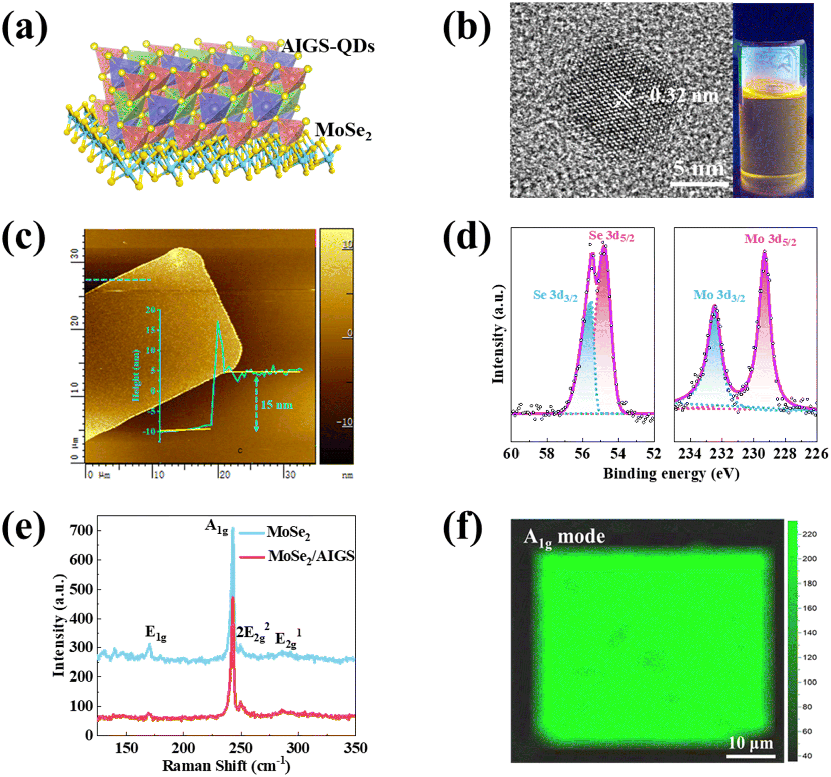 | ||
| Fig. 1 Characteristics of AIGS-QDs, MoSe2, and MoSe2/AIGS-QDs heterojunctions. (a) Schematic representation of the crystal structure of the MoSe2/AIGS-QDs heterojunction. (b) HRTEM image of AIGS-QDs. Inset: photograph of the AIGS-QDs solution under UV radiation (365 nm). (c) AFM image of the MoSe2. Inset: the thickness of MoSe2. (d) XPS of Mo and Se. (e) Raman spectra of MoSe2 and MoSe2/AIGS-QDs heterojunctions. (f) Raman mapping of MoSe2 (A1g mode). | ||
X-ray photoemission spectroscopy (XPS) is employed to identify the elemental composition and electron binding energy in AIGS-QDs. The XPS analysis of AIGS-QDs is presented in Fig. S4,† which reveals the presence of four major elements. There are two peaks observed at 371 eV and 365 eV, which can be attributed to the Ag 3d3/2 and Ag 3d5/2 orbitals, respectively. The 3d spectra of indium (In) exhibit two prominent peaks located at 449.5 eV and 441.9 eV, which align with the distinctive In 3d3/2 and In 3d5/2 orbitals, respectively. The peaks observed at 1141.8 eV and 1114.8 eV correspond to the Ga 2p1/2 and Ga 2p3/2 orbitals, respectively. In addition, the S 2p1/2 and S 2p3/2 orbitals exhibit energies of approximately 160 eV and 158.7 eV, respectively. All of these results are in accord with the previous reports of AIGS-QDs.34,39
The MoSe2 was grown by the selenylation method using Se power precursors and Mo film. To confirm the MoSe2 thin film quality, Atomic Force Microscope (AFM), XPS and Raman images were gained. The thickness of MoSe2 was verified at about 15 nm by AFM (Fig. 1c), which shows smooth surfaces of the samples and is similar to previous report.40,41 The optical microscope (OM) photograph of a square MoSe2 film displayed in Fig. S5† appears uniform color. XPS measurements were introduced to further characterize the MoSe2 film. The elements of Mo, Se, O and C can be identified in Fig. S6.† XPS spectra of the two primary elements of Mo and Se in the MoSe2 film are presented in Fig. 1d. The two peaks at 229.3 eV and 232.4 eV correspond to the Mo 3d5/2 and 3d3/2 orbitals. Similarly, the 3d spectra of Se show two major peaks located at 54.8 eV and 55.5 eV, consistent with the characteristic Se 3d5/2 and 3d3/2 orbitals, respectively, which are in agreement with the previous work.42,43
The Raman spectra of MoSe2 and MoSe2/AIGS-QDs were excited under 532 nm and presented in Fig. 1e to provide additional insights into the structure and composition of MoSe2. The MoSe2 sample presents a dominant Raman peak at approximately 242.0 cm−1, which corresponds to an out-of-plane Raman mode known as the A1g mode. Three additional peaks are observed at approximately 169.1 cm−1, 249.6 cm−1, and 285.7 cm−1, respectively. These peaks correspond to the vibration modes of in-plane modes E1g, 2E22g, and E12g, which are consistent with previous research results.44,45 The A1g mode of MoSe2 flake exhibits the highest intensity due to the strong interlayer interaction. Meanwhile, a higher peak intensity of the A1g mode generally indicates a lower number of layers.45 The presence of a distinct peak in the sharp A1g mode confirms the high quality of the MoSe2 sheeting. To comprehensively understand the quality of selenylation, a Raman mapping of MoSe2 was collected around the A1g mode (242.0 cm−1), as displayed in Fig. 1f. It is noteworthy to mention that the uniform intensity observed across the whole area (50 μm × 50 μm) of the MoSe2 thin film indicates the consistent thickness. Furthermore, when the AIGS-QDs were spun on the surface of MoSe2 (Fig. S7†), no new peaks were observed, suggesting that the AIGS-QDs layer does not disrupt the structure of MoSe2.46 Consequently, these results demonstrate the successful preparation of high-quality AIGS-QDs/MoSe2 heterojunction, which can be used as the response materials in the photodetector.
To assess the optical properties of the MoSe2/AIGS-QDs heterojunction, the absorption spectrum, PL, PL mapping, and TRPL were recorded. The UV-vis absorption spectra of the pure AIGS-QDs, MoSe2, and hybrid MoSe2/AIGS-QDs samples were measured, as depicted in Fig. 2a. The absorption spectrum of MoSe2 displays a broad absorption range spanning from 300 to 800 nm. When the AIGS-QDs were coated on the MoSe2 film, the MoSe2 film exhibited a significantly enhanced absorption in the wavelength range of 300–480 nm, which is attributed to the cooperative absorption of AIGS-QDs and the MoSe2 layers. This high absorption of the hybrid MoSe2/AIGS-QDs heterojunction indicates its potential for application in the field of photodetectors.47,48
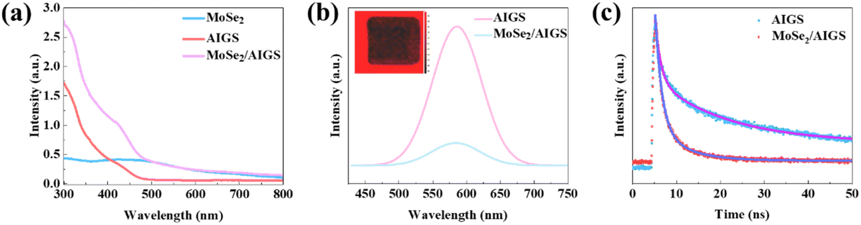 | ||
| Fig. 2 Optical properties of the MoSe2 and MoSe2/AIGS-QDs heterojunction. (a) UV-vis absorption spectra of the MoSe2, AIGS-QDs, and MoSe2/AIGS-QDs. (b) PL spectra of AIGS-QDs and MoSe2/AIGS-QDs. Inset: the PL mapping of the MoSe2 that was covered with AIGS-QDs (the red zone is only AIGS-QDs and the dark zone is MoSe2 coupling with AIGS-QDs). (c) TRPL decay transients measured at 570 nm for AIGS-QDs and MoSe2/AIGS-QDs. | ||
The PL spectra of AIGS-QDs and MoSe2/AIGS-QDs heterostructure were obtained with photoexcitation at 3.8 eV (325 nm) and emerged in Fig. 2b. There is a peak around 577 nm in PL of pure AIGS-QDs. After being coupled with MoSe2, there exhibits a significant quenching of about 84% reduction compared with that of the pristine AIGS-QDs. This phenomenon explains that a large number of photon-generated carriers may be transferred between AIGS-QDs and MoSe2.49 The PL mapping was measured to further reveal the charge exchange between AIGS-QDs and MoSe2. As shown in the inset of Fig. 2b, the zone of QDs was bright (red color) but the zone of MoSe2 was dark square, which illustrates that MoSe2 has a strong quenching of PL on AIGS-QDs. This PL quenching is associated with the charge transfer at the interface of the AIGS-QDs and MoSe2 heterojunction.50
To comprehensively elucidate the charge transfer dynamics occurring at the interfaces between MoSe2 and AIGS-QDs, TRPL measurements were utilized. The TRPL decay curves in Fig. 2c were fitted using a biexponential decay equation to determine the lifetime of both AIGS-QDs and the MoSe2/AIGS-QDs heterostructure. The pristine AIGS-QDs exhibited a significantly long PL lifetime of 15.84 ns, indicating slow recombination of carriers in the AIGS-QDs. However, when coupled with MoSe2, the lifetime (τ) decreases significantly from 15.84 to 4.46 ns, suggesting a substantial charge transfer occurring at the interface between AIGS-QDs and MoSe2.48,51 Under light illumination, photogenerated electrons exhibit a strong tendency to transfer from AIGS-QDs to MoSe2, while the generated holes remain in AIGS-QDs, forming the separation of the electrons and holes. This charge transfer results in a reduced probability of recombination51 and the accumulation of unpaired electrons and holes, leading to strong quenching and the shortened lifetime of the PL. Meanwhile, charge transfer is beneficial to the electrons and holes separation at the interface of the heterojunction, which is advantageous for enhancing the photocurrent. The strong optical absorption and effective charge transfer demonstrate that MoSe2/AIGS-QDs heterojunction is a promising application in photodetector.
The schematic diagram and practical optical image of the MoSe2 and MoSe2/AIGS-QDs photodetector device are depicted in Fig. 3a. To compare the photoelectric detection performance between MoSe2 devices with and without AIGS-QDs, the output curves were plotted in Fig. 3b and c. Both the I–V curves of the MoSe2 and MoSe2/AIGS-QDs heterostructure device are linear, which implies a good ohmic contact between Cr/Au electrodes and MoSe2 (or MoSe2/AIGS-QDs). The dark current of the original and heterojunction devices is measured to be approximately 0.706 μA and 0.931 μA, respectively, at a source-drain voltage (Vds) of 3 V. Under light irradiation (illuminated by a 442 nm laser at 11.936 mW cm−2), the output current of the MoSe2 heterojunction device increased from 0.706 μA to 0.795 μA, compared with that in the dark. After being coupled with AIGS-QDs, the output current of the hybrid device increases to 1.099 μA. The photocurrents (Iph = Ilight − Idark) of the device were calculated in Fig. 3d. Both the photocurrents of the pure MoSe2 device and the hybrid device exhibit a monotonic increase with increasing optical power intensity. It is worth pointing out that after combining with QDs, the photocurrent is two times larger than that of the pristine MoSe2 photodetector. This phenomenon demonstrates that the integration of AIGS-QDs with MoSe2 leads to an increase in photocurrent in hybrid devices. These results suggest that the photosensitizing layer AIGS-QDs can effectively improve the performance of the MoSe2 photodetector.
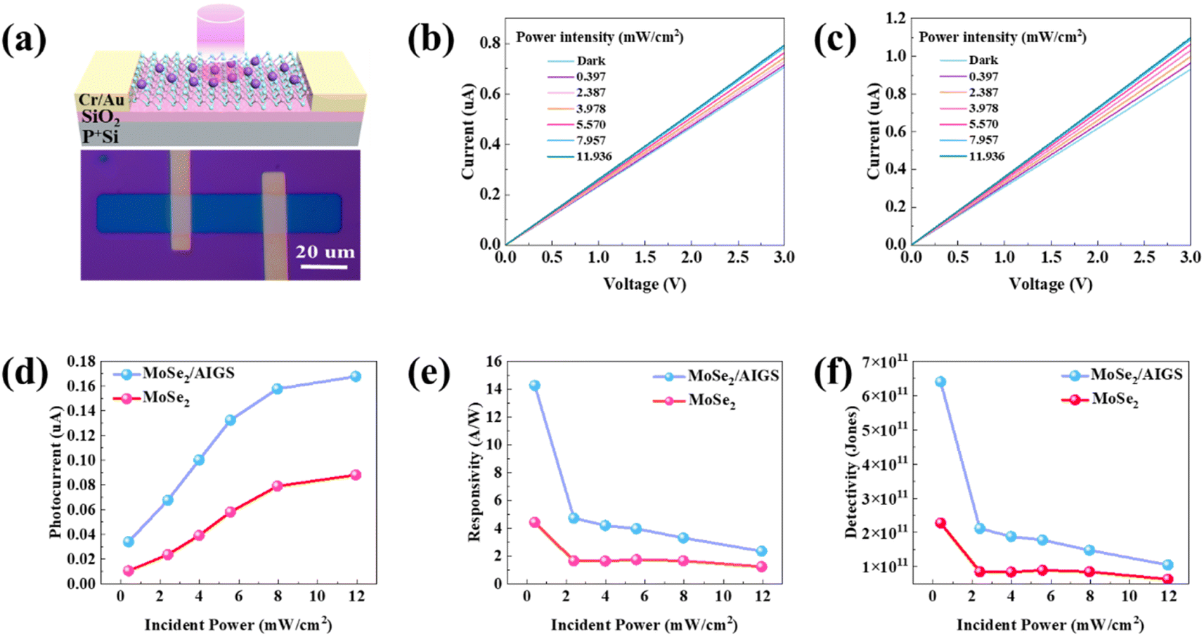 | ||
| Fig. 3 Photoelectric response characteristics of the MoSe2 and MoSe2/AIGS-QDs heterojunction device under 442 nm illumination. (a) Schematic diagram and optical image of the hybrid photodetector. (b and c) Output current of the MoSe2 and hybrid MoSe2/AIGS-QDs photodetector measured under different power intensities. (d–f) Photocurrent, responsivity and specific detectivity of the MoSe2 and hybrid MoSe2/AIGS-QDs photodetector measured at Vds = 3 V under different power intensities. | ||
To evaluate the device performance of the photocurrent in individual MoSe2 and heterojunction photodetector, two important indicators, namely responsivity (R) and specific detectivity (D*), are introduced. These indicators play a crucial role in determining the performance of photodetectors.
The photoelectric conversion capability of the device, denoted as R, was evaluated with a wavelength of 442 nm under various incident power intensities at 3 V. The responsivity was calculated using the formula R = Iph/PS,52–54 where Iph represents the photocurrent, P denotes the incident power intensity, and S represents the area of the device channel with dimensions of 30 μm length and 20 μm width. As shown in Fig. 3e, there is a decrease in the responsivity of both devices as the incident power intensity increases. This trend may be attributed to the lower recombination probability of carriers at lower incident power intensity.55 The highest responsivity was found at the minimum incident power intensity (0.357 mW cm−2) for the MoSe2 device is about 4.42 A W−1. Once the AIGS-QDs were coated on the MoSe2 surface, the responsivity was calculated to be 14.3 A W−1, which is improved more than three times compared to that of the MoSe2 photodetector. This value is at a higher level compared with those in previous work, such as MoS2/PbS-QDs (0.6 A W−1),29 WSe2/CdSe-QD (9.27 A W−1),56 and MoS2/ZnO-QDs (0.084 A W−1).57 These results demonstrate our hybrid 2D/QDs device presents a potential replacement for toxic hybrid photodetectors with excellent performance.
In addition, the D* is another crucial parameter for assessing the capability of signal detection in the presence of noise. It is defined as D* = RS1/2/(2eIdark)1/2, where S represents the effective detection area of the device, e denotes the electronic charge, and Idark corresponds to the dark current, as illustrated in Fig. 3f.58,59 Similar to R, the maximum value of D* for the device is observed at the minimum light power. After being deposited with the AIGS-QDs layer, the D* value of the heterojunction device increases three times compared to that of the MoSe2 device (from 2.28 × 10¹¹ Jones to 6.4 × 10¹¹ Jones). Furthermore, the D* value of the MoSe2/AIGS-QDs device is superior to those of previously reported 2D/0D photodetectors. For instance, the D* value of WSe2/CdSe-QD was reported to be 4.38 × 10¹⁰ Jones,56 MoS2/PbS-QDs had a D* value of 1 × 10¹¹ Jones,60 and graphene/WS2-QDs exhibited a D* value of 8.9 × 10⁸ Jones.61 These results indicate that the MoSe2/AIGS-QDs photodetector shows promising application prospects in detecting low light intensity.
To gain a deeper comprehension of the charge transfer mechanism, ultraviolet photo-electron spectroscopy (UPS) was employed to elucidate the energy band structures of the AIGS-QDs and MoSe2, as depicted in Fig. 4a and b. The work function (WF) refers to the energy of the highest occupied states and can be determined using the equation WF = hν − Eonset,67,68 where hν = 21.21 eV represents the energy of the incident photon and Eonset corresponds to the onset level associated with the secondary electrons. According to the UPS results, the work function (WF) values of AIGS-QDs and MoSe2 were estimated to be 3.21 eV and 4.81 eV, respectively. Subsequently, the energy of the valence band maximum (EVBM) of AIGS-QDs and MoSe2 is calculated to be 1.2 eV and 0.84 eV, respectively. Furthermore, the energy values for the conduction band minimum (ECBM) are determined to be 2.08 eV and 4.55 eV, based on the fitting of the optical bandgaps with the absorption spectrum (Fig. S8†). In conclusion, the energy band alignment diagrams of AIGS-QDs and MoSe2 (Fig. 4b) indicate that the MoSe2/AIGS-QDs heterojunction forms a type II band alignment heterojunction.51
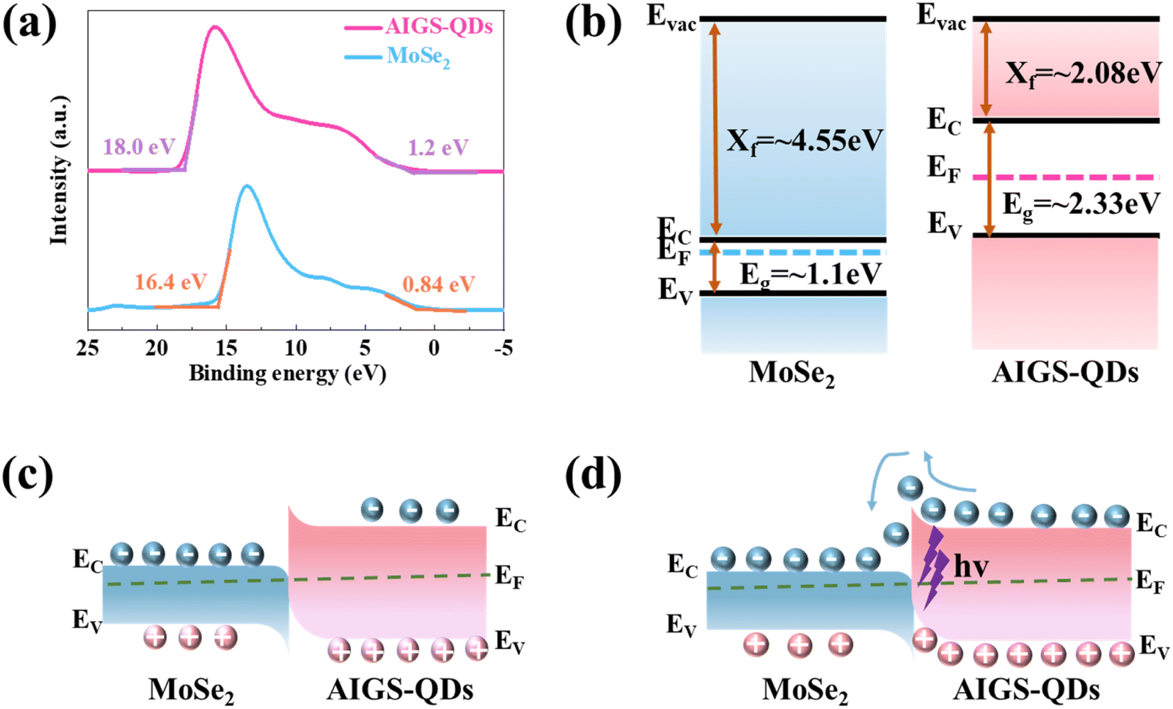 | ||
| Fig. 4 Charge transfer mechanism. (a) Ultraviolet photoelectron spectroscopy (UPS) measurement results of AIGS-QDs and MoSe2. (b) Energy band diagram of MoSe2 (left) and AIGS-QDs (right). (c and d) Mechanism of charge-carrier injection between AIGS-QDs and MoSe2 in contact state under dark and contact state under illumination. | ||
The increased responsivity and detectivity observed in the MoSe2/AIGS heterojunction photodetector, as compared to the MoSe2 device, are attributed to the type II energy band alignment. When the AIGS-QDs come into contact with MoSe2 (Fig. 4c) and form a heterojunction, the difference in Fermi levels causes electrons and holes at the interface to diffuse and drift, aligning the Fermi level and establishing a new equilibrium. This results in the bending of the energy band and the formation of a depletion region, creating a built-in field.57,69 Under illumination (Fig. 4d), AIGS-QDs absorb photon energy and generate electron–hole pairs. Subsequently, these pairs are efficiently separated by the inherent electric field at the interface of the heterojunction. As a consequence, the transfer of electrons occurs towards the MoSe2 side, while holes remain on the AIGS-QDs side. As a consequence, the transfer of electron–hole pairs from AIGS-QDs to MoSe2 leads to a substantial improvement in responsivity and detectivity.67,68
To comprehensively evaluate the photoelectric performances of the MoSe2/AIGS-QDs device, we have compared our work with similar studies and summarized the results in Table 1. The MoSe2/AIGS-QDs device demonstrates outstanding responsivity and detectivity, highlighting its exceptional photo-response properties.
| Layer thickness | Measurement condition (nm) | R (A W−1) | D* (Jones) | References | |
|---|---|---|---|---|---|
| MoS2/PbS-QDs | 8 nm | 400–1600 | 0.6 | 1012 | 29 |
| WSe2/CdSe-QD | 1.019 nm (CVD) | 638 | 9.27 | 4.38 × 10¹⁰ | 56 |
| MoS2/ZnO-QDs | Monolayer (CVD) | 405 | 0.084 | 1.05 × 10¹¹ | 57 |
| Graphene/WS2 QDs | Monolayer (CVD) | 365 | 3.1 × 10² | 8.9 × 10⁸ | 61 |
| MoSe2/CsPb(Cl/Br)3-QDs | Few-layer | 455 | 104 | — | 62 |
| MoSe2 | Few-layer | 455 | 34 | — | 62 |
| MoSe2 | Monolayer | 514 | 0.32 | 3.54 × 10¹² | 63 |
| MoSe2 | 44 nm | 785 | 238 | 7.6 × 10¹¹ | 64 |
| MoS2/PbSe-QDs | 4.02 nm | 1310 | 137.6 | 7.7 × 10¹⁰ | 65 |
| n-WS2/p-PbS QDs | Multilayer | 1550 | 0.18 | 4.11 × 10¹¹ | 66 |
| MoSe2 | 15 nm | 442 | 4.42 | 2.28 × 10¹¹ | This work |
| MoSe2/AIGS-QDs | 15 nm | 442 | 14.3 | 6.4 × 10¹¹ | This work |
4. Conclusions
In summary, the sensitizing layer AIGS-QDs were successfully integrated into the MoSe2 surface to form a high-performance photodetector. The difference in the Fermi level enables the transfer of charges from AIGS-QDs to MoSe2, resulting in a strong quenching of the PL of AIGS-QDs and a shortening in the decay time of PL in the MoSe2/AIGS-QDs heterojunction. The photodetector with MoSe2/AIGS-QDs heterojunction demonstrates exceptional performance attributed to its efficient charge transfer at the interface. It exhibits a responsivity of 14.3 A W−1 and a specific detectivity of 6.4 × 10¹¹ Jones. The responsivity and detectivity of the hybrid phototransistor are significantly enhanced by more than three times compared with that of the MoSe2 photodetector. The results present that the incorporation of AIGS-QDs sensitizing layer into MoSe2 can significantly enhance the optoelectronic performance of MoSe2 devices, making it a promising candidate for high-performance photodetector applications.Author contributions
XJZ and XSW contribute equally to this work. XJZ, XSW, RMJ and YHL grow the samples and fabricate the devices. XJZ, XSW, and RMJ conduct AFM, Raman, absorption spectrum and PL measurement. XJZ and YHL conduct Raman mapping and PL mapping measurement. TTG, XDH, LXW, and TZ, DNY help picture the device diagram and analysis of the XRD data. XJZ and XSW initiate the project and write the manuscript. XFS and XC provide grammar and word modification suggestions for the manuscript. XFS and XC provide suggestions and funding for the research. All authors discussed the results and approved the final version of the manuscript.Conflicts of interest
The authors declare no conflicts of interest.Acknowledgements
This work was financially supported by the National Natural Science Foundation of China (62274089, 52372152, 92064007) and the Taishan Industrial Leading Talents Project.References
- J. Wang, F. Ma and M. Sun, RSC Adv., 2017, 7, 16801–16822 RSC.
- L. Wang, Z. F. Ren, K. Y. Wang, S. J. He and L. B. Luo, Mater. Res. Express, 2017, 4, 045022 CrossRef.
- X. Hong, Y. Huang, Q. Tian, S. Zhang, C. Liu, L. Wang, K. Zhang, J. Sun, L. Liao and X. Zou, Adv. Sci., 2022, 9, 2202019 CrossRef CAS PubMed.
- M. K. Zhang, W. D. Liu, Y. P. Gong, Q. Liu and Z. G. Chen, Adv. Opt. Mater., 2022, 10, 2201889 CrossRef CAS.
- A. Pelella, A. Grillo, E. Faella, G. Luongo, M. B. Askari and A. Di Bartolomeo, ACS Appl. Mater. Interfaces, 2021, 13, 47895–47903 CrossRef CAS PubMed.
- J. Li, C. Zhao, B. Liu, C. You, F. Chu, N. Tian, Y. Chen, S. Li, B. An, A. Cui, X. Zhang, H. Yan, D. Liu and Y. Zhang, Appl. Surf. Sci., 2019, 473, 633–640 CrossRef CAS.
- F. Zhang, X. Chen, Z. Zuo, X. Qin, X. Xu and X. Zhao, J. Mater. Sci.: Mater. Electron., 2018, 29, 5180–5185 CrossRef CAS.
- H. Zhong, L. Tang, P. Tian, L. Yu, W. Zuo and K. S. Teng, Sensors, 2023, 23(4), 2254 CrossRef CAS PubMed.
- D. H. Kwak, P. Ramasamy, Y. S. Lee, M. H. Jeong and J. S. Lee, ACS Appl. Mater. Interfaces, 2019, 11, 29041–29046 CrossRef CAS PubMed.
- H. J. Lee, S. Im, D. Jung, K. Kim, J. A. Chae, J. Lim, J. W. Park, D. Shin, K. Char, B. G. Jeong, J. S. Park, E. Hwang, D. C. Lee, Y. S. Park, H. J. Song, J. H. Chang and W. K. Bae, Nat. Commun., 2023, 14, 3779 CrossRef PubMed.
- X. Song, Y. Jian, X. Wang, J. Chen, Q. Shan, S. Zhang, Z. Chen, X. Chen and H. Zeng, Nanotechnology, 2023, 34, 195201 CrossRef PubMed.
- S. Goossens, G. Navickaite, C. Monasterio, S. Gupta, J. J. Piqueras, R. Pérez, G. Burwell, I. Nikitskiy, T. Lasanta, T. Galán, E. Puma, A. Centeno, A. Pesquera, A. Zurutuza, G. Konstantatos and F. Koppens, Nat. Photonics, 2017, 11, 366–371 CrossRef CAS.
- G. Konstantatos, M. Badioli, L. Gaudreau, J. Osmond, M. Bernechea, F. P. G. de Arquer, F. Gatti and F. H. L. Koppens, Nat. Nanotechnol., 2012, 7, 363–368 CrossRef CAS PubMed.
- Z. T. Hu, T. Gan, L. Du, J. Z. Zhang, H. Xu, S. L. Han, H. L. Xu, F. Liu, Y. P. Chen and G. Chen, J. Infrared, Millimeter, Terahertz Waves, 2019, 38, 269–274 CAS.
- J. J. Zheng, Y. R. Wang, K. H. Yu, X. X. Xu, X. X. Sheng, E. T. Hu and W. Wei, Acta Phys. Sin., 2018, 67, 118502 CrossRef.
- F. X. Liang, Y. Gao, C. Xie, X. W. Tong, Z. J. Li and L. B. Luo, J. Mater. Chem. C, 2018, 6, 3815–3833 RSC.
- H. Yao, X. Guo, A. Bao, H. Mao, Y. Ma and X. Li, Chin. Phys. B, 2022, 31, 038501 CrossRef.
- M. Ye, D. Zhang and Y. K. Yap, Electronics, 2017, 6, 43 CrossRef.
- W. Choi, N. Choudhary, G. H. Han, J. Park, D. Akinwande and Y. H. Lee, Mater. Today, 2017, 20, 116–130 CrossRef CAS.
- P. V. Pham, S. C. Bodepudi, K. Shehzad, Y. Liu, Y. Xu, B. Yu and X. Duan, Chem. Rev., 2022, 122, 6514–6613 CrossRef CAS PubMed.
- Z. Zhu, I. Murtaza, H. Meng and W. Huang, RSC Adv., 2017, 7, 17387–17397 RSC.
- D. M. Geum, S. Kim, J. Khym, J. Lim, S. Kim, S. Y. Ahn, T. S. Kim, K. Kang and S. Kim, Small, 2021, 17, 2007357 CrossRef CAS PubMed.
- C. Song, G. Noh, T. S. Kim, M. Kang, H. Song, A. Ham, M. kyung Jo, S. Cho, H. J. Chai, S. R. Cho, K. Cho, J. Park, S. Song, I. Song, S. Bang, J. Y. Kwak and K. Kang, ACS Nano, 2020, 14, 16266–16300 CrossRef CAS PubMed.
- H. S. Nalwa, RSC Adv., 2020, 10, 30529–30602 RSC.
- H. Li, K. Zhang, X. Li, B. Liu, L. Li, Z. Mei, T. Chen, Q. Liu, W. Yu, J. Yuan, H. Mu and S. Lin, Mater. Des., 2023, 227, 111799 CrossRef CAS.
- A. Grillo, Z. Peng, A. Pelella, A. Di Bartolomeo and C. Casiraghi, ACS Nano, 2023, 17, 1533–1540 CrossRef CAS PubMed.
- S. Zhang, X. Wang, Y. Chen, G. Wu, Y. Tang, L. Zhu, H. Wang, W. Jiang, L. Sun, T. Lin, H. Shen, W. Hu, J. Ge, J. Wang, X. Meng and J. Chu, ACS Appl. Mater. Interfaces, 2019, 11, 23667–23672 CrossRef CAS PubMed.
- C. Hu, D. Dong, X. Yang, K. Qiao, D. Yang, H. Deng, S. Yuan, J. Khan, Y. Lan, H. Song and J. Tang, Adv. Funct. Mater., 2017, 27, 1603605 CrossRef.
- S. Mukherjee, S. Jana, T. K. Sinha, S. Das and S. K. Ray, Nanoscale Adv., 2019, 1, 3279–3287 RSC.
- L. Yu, P. Tian, L. Tang, W. Zuo, H. Zhong, Q. Hao, K. S. Teng, G. Zhao, R. Su, X. Gong and J. Yuan, Sensors, 2023, 23(9), 4328 CrossRef CAS PubMed.
- M. M. Ackerman, X. Tang and P. Guyot Sionnest, ACS Nano, 2018, 12, 7264–7271 CrossRef CAS PubMed.
- H. Kan, S. Liu, B. Xie, B. Zhang and S. Jiang, J. Mater. Sci.: Mater. Electron., 2017, 28, 9782–9787 CrossRef CAS.
- Z. Hu, H. Lu, W. Zhou, J. Wei, H. Dai, H. Liu, Z. Xiong, F. Xie, W. Zhang and R. Guo, J. Mater. Sci. Technol. Res., 2023, 134, 189–196 CrossRef CAS.
- W. Hoisang, T. Uematsu, T. Torimoto and S. Kuwabata, Nanoscale Adv., 2022, 4, 849–857 RSC.
- G. Huang, Y. Huang, Z. Liu, J. Wei, Q. Zhu, G. Jiang, X. Jin, Q. Li and F. Li, J. Lumin., 2021, 233, 117903 CrossRef CAS.
- J. H. Kim, B. Y. Kim, E. P. Jang, S. Y. Yoon, K. H. Kim, Y. R. Do and H. Yang, Chem. Eng. J., 2018, 347, 791–797 CrossRef CAS.
- G. Huang, Y. Huang, Z. Liu, J. Wei, Q. Zhu, G. Jiang, X. Jin, Q. Li and F. Li, J. Lumin., 2021, 233, 117903 CrossRef CAS.
- H. J. Lee, S. Im, D. Jung, K. Kim, J. A. Chae, J. Lim, J. W. Park, D. Shin, K. Char, B. G. Jeong, J. S. Park, E. Hwang, D. C. Lee, Y. S. Park, H. J. Song, J. H. Chang and W. K. Bae, Nat. Commun., 2023, 14, 3779 CrossRef PubMed.
- W. Hoisang, T. Uematsu, T. Torimoto and S. Kuwabata, Inorg. Chem., 2021, 60, 13101–13109 CrossRef CAS PubMed.
- W. Du, P. Yu, J. Zhu, C. Li, H. Xu, J. Zou, C. Wu, Q. Wen, H. Ji, T. Liu, Y. Li, G. Zou, J. Wu and Z. M. Wang, Nanotechnology, 2020, 31, 225201 CrossRef CAS PubMed.
- A. Bala, B. So, P. Pujar, C. Moon and S. Kim, ACS Nano, 2023, 17, 4296–4305 CrossRef CAS PubMed.
- W. A. Abdallah and A. E. Nelson, J. Mater. Sci., 2005, 40, 2679–2681 CrossRef CAS.
- X. Zhao, J. Sui, F. Li, H. Fang, H. Wang, J. Li, W. Cai and G. Cao, Nanoscale, 2016, 8, 17902–17910 RSC.
- S. Y. Chen, C. Zheng, M. S. Fuhrer and J. Yan, Nano Lett., 2015, 15, 2526–2532 CrossRef CAS PubMed.
- P. Tonndorf, R. Schmidt, P. Böttger, X. Zhang, J. Börner, A. Liebig, M. Albrecht, C. Kloc, O. Gordan, D. R. T. Zahn, S. Michaelis de Vasconcellos and R. Bratschitsch, Opt. Express, 2013, 21, 4908–4916 CrossRef CAS PubMed.
- X. Wang, D. Yan, C. Zhu, Y. Feng, T. Guo, R. Jia, K. Qu, L. Li, T. Zhao, Y. Xiong, A. Farhan, Y. Lin, L. Wu, Y. Dong, S. Zhang, X. Chen and X. Song, 2D Mater., 2023, 10, 045020 CrossRef.
- M. Peng, X. Xie, H. Zheng, Y. Wang, Q. Zhuo, G. Yuan, W. Ma, M. Shao, Z. Wen and X. Sun, ACS Appl. Mater. Interfaces, 2018, 10, 43887–43895 CrossRef CAS PubMed.
- Q. Zhang, F. Yang, S. Zhou, N. Bao, Z. Xu, M. Chaker and D. Ma, Appl. Catal., B, 2020, 270, 118879 CrossRef CAS.
- A. Bora, S. Paul, M. T. Hossain and P. K. Giri, J. Phys. Chem. C, 2022, 126, 12623–12634 CrossRef CAS.
- M. T. Hossain, L. P. L. Mawlong, T. Jena, A. Bora, U. Nath, M. Sarma and P. K. Giri, ACS Appl. Nano Mater., 2023, 6, 11023–11036 CrossRef CAS.
- H. Wu, Z. Kang, Z. Zhang, Z. Zhang, H. Si, Q. Liao, S. Zhang, J. Wu, X. Zhang and Y. Zhang, Adv. Funct. Mater., 2018, 28, 1802015 CrossRef.
- T. Shen, F. Li, Z. Zhang, L. Xu and J. Qi, ACS Appl. Mater. Interfaces, 2020, 12, 54927–54935 CrossRef CAS PubMed.
- J. Qiao, F. Feng, S. Song, T. Wang, M. Shen, G. Zhang, X. Yuan and M. G. Somekh, Adv. Funct. Mater., 2022, 32, 2110706 CrossRef CAS.
- J. K. Qin, D. D. Ren, W. Z. Shao, Y. Li, P. Miao, Z. Y. Sun, P. Hu, L. Zhen and C. Y. Xu, ACS Appl. Mater. Interfaces, 2017, 9, 39456–39463 CrossRef CAS PubMed.
- A. Xie, Y. Jian, Z. Cheng, Y. Gu, Z. Chen, X. Song and Z. Yang, J. Phys.: Condens.Matter, 2022, 34, 154007 CrossRef CAS PubMed.
- H. Meng, F. Zhang, Z. Mo, Q. Xia, M. Zhong and J. He, J. Phys. D, 2022, 55, 444006 CrossRef.
- Y. H. Zhou, Z. B. Zhang, P. Xu, H. Zhang and B. Wang, Nanoscale Res. Lett., 2019, 14, 364 CrossRef PubMed.
- S. Qin, K. Li, J. Zhu, H. Xu, N. Ali, A. Rahimi-Iman and H. Wu, J. Alloys Compd., 2021, 856, 158179 CrossRef CAS.
- R. Ghosh, Y. S. Kang, K. Yadav, H. Lin, Z. L. Yen, H. Y. Lin, G. Z. Lu, R. Sankar, Y.-P. Hsieh, M. Hofmann and Y. F. Chen, ACS Appl. Electron. Mater., 2022, 4, 5208–5214 CrossRef CAS.
- S. Pak, Y. Cho, J. Hong, J. Lee, S. Lee, B. Hou, G. H. An, Y.-W. Lee, J. E. Jang, H. Im, S. M. Morris, J. I. Sohn, S. Cha and J. M. Kim, ACS Appl. Mater. Interfaces, 2018, 10, 38264–38271 CrossRef CAS PubMed.
- S. Mukherjee, D. Bhattacharya, S. Patra, S. Paul, R. K. Mitra, P. Mahadevan, A. N. Pal and S. K. Ray, ACS Appl. Mater. Interfaces, 2022, 14, 5775–5784 CrossRef CAS PubMed.
- S. Lee, J. Y. Kim, S. Choi, Y. Lee, K. S. Lee, J. Kim and J. Joo, ACS Appl. Mater. Interfaces, 2020, 12, 25159–25167 CrossRef CAS PubMed.
- Md. S. Hassan, S. Bera, D. Gupta, S. K. Ray and S. Sapra, ACS Appl. Mater. Interfaces, 2019, 11, 4074–4083 CrossRef CAS PubMed.
- P. J. Ko, A. Abderrahmane, N. H. Kim and A. Sandhu, Semicond. Sci. Technol., 2017, 32, 065015 CrossRef.
- B. Kundu, O. Özdemir, M. Dalmases, G. Kumar and G. Konstantatos, Adv. Opt. Mater., 2021, 9, 2101378 CrossRef CAS.
- S. Kim, D. Lee, S. Moon, J. Choi, D. Kim, J. Kim and S. Baek, Adv. Funct. Mater., 2023, 33, 2303778 CrossRef CAS.
- Y. Pak, S. Mitra, N. Alaal, B. Xin, S. Lopatin, D. Almalawi, J.-W. Min, H. Kim, W. Kim, G. Y. Jung and I. S. Roqan, Appl. Phys. Lett., 2020, 116, 112102 CrossRef CAS.
- H. Wu, H. Si, Z. Zhang, Z. Kang, P. Wu, L. Zhou, S. Zhang, Z. Zhang, Q. Liao and Y. Zhang, Adv Sci, 2018, 5, 1801219 CrossRef PubMed.
- Y. Wu, S. E. Wu, J. Hei, L. Zeng, P. Lin, Z. Shi, Q. Chen, X. Li, X. Yu and D. Wu, Nano Res., 2023, 16, 11422–11429 CrossRef CAS.
Footnotes |
| † Electronic supplementary information (ESI) available. See DOI: https://doi.org/10.1039/d3ra07240a |
| ‡ These authors contributed equally to this work. |
| This journal is © The Royal Society of Chemistry 2024 |