DOI:
10.1039/D3RA06860A
(Paper)
RSC Adv., 2024,
14, 1634-1648
Morphological, structural, optical and dielectric analysis of Cs2TiBr6 perovskite nanoparticles
Received
9th October 2023
, Accepted 14th December 2023
First published on 4th January 2024
Abstract
In the pursuit of lead-free perovskite materials suitable for harnessing solar energy, a recent discovery has emerged regarding Cs2TiBr6. This compound has garnered attention as a prospective candidate, exhibiting favorable optical and electrical characteristics alongside exceptional resilience when subjected to environmental strains. This study details the successful synthesis of non-hazardous metal halide nanoparticles of Cs2TiBr6 via the slow cooling method. Comprehensive investigations into the structural, optical, and dielectric characteristics have been undertaken. The temperature sensitivity of various electrical properties, including the dielectric constant, loss factor, electric modulus, and AC/DC conductivity, is evident in this perovskite material. This phenomenon is observed across a frequency range of 1 to 107 Hz. Furthermore, examination of the Nyquist plot highlights the distinctive contributions of both grain and grain boundaries to the overall impedance characteristics. In the high-frequency range, it is observed that the dielectric constant exhibits an upward trend as the temperature rises. Examination of the adapted Cole–Cole plot unveils that both space charge and free charge conductivity escalate with increasing temperature, while concurrently, the relaxation time experiences a reduction with the temperature's ascent. We observed an asymmetrical pattern in the electric modulus spectra at varying temperatures using a modified Kohlrausch–Williams–Watts equation. This asymmetry is consistent with the inherent non-Debye nature of perovskite materials. Additionally, as the temperature increases, we note a shift in the imaginary component of the electric modulus spectra, transitioning from a non-Debye character towards a semi-Debye nature, though it does not achieve a strictly Debye-type response. This transformation indicates the semiconducting properties of the material. We elucidate the AC conductivity behavior in Cs2TiBr6 by employing the non-overlapping small-polaron tunneling (NSPT) mechanism as the basis. The activation energy, as determined from both the modulus spectra and DC conductivity, aligns closely, providing robust evidence for the congruence between the relaxation dynamics and the conduction mechanism. In addition to these attributes, Cs2TiBr6 exhibits a substantial dielectric constant coupled with negligible dielectric loss, thus establishing its potential suitability for energy harvesting devices.
1. Introduction
A significant challenge hindering the practical use and advancement of metal halide perovskites pertains to the harmful nature of their primary component, lead (Pb).1–3 The adverse impacts of lead on the environment and human well-being have raised substantial concerns, underscored by prevailing regulations in various countries that restrict the use of heavy metals.4 Consequently, there exists a continually increasing fascination with innovative lead-free halide perovskite configurations, encompassing both bulk films and nanocrystals (NCs).5,6 Nonetheless, nearly all the investigated substitutes for lead are reliant on materials with disputed levels of toxicity, modest stability, and/or restricted accessibility, thereby presenting challenges in terms of disposal and recycling.7
Titanium (Ti) emerges as an environmentally friendly and readily available element, holding promise as an optimal component in sustainable perovskite formulations. In a recent study, Ju and colleagues delved into an emerging group of vacancy-arranged double perovskite structures featuring Ti(IV) as the central element, characterized by the chemical formula A2TiX6. Through a comprehensive blend of theoretical and empirical investigations, the Cs2TiBr6 perovskite, boasting a band gap of approximately 1.8 eV, has demonstrated its potential viability in the realm of photovoltaic applications.8 In a separate study, the authors previously established that thin films of Cs2TiBr6 exhibit effective photoluminescence (PL), extended carrier-diffusion distances, and energy levels well-suited for use in tandem photovoltaic systems.9 Furthermore, the integration of Cs2TiBr6 into solar cells resulted in a consistent power conversion efficiency (PCE) reaching 3.3%, marking one of the most elevated PCE values documented for double perovskites. Additionally, the authors underscored the remarkable inherent stability of Cs2TiBr6, both under environmental conditions (such as heat, moisture, and light) and intrinsically.10 This stability was achieved through the vapor deposition synthesis method conducted at elevated temperatures. The initial investigations into Ti-based perovskites, shedding light on their capacity to pave the way for the creation of genuinely environmentally sustainable and resilient solar cells, have garnered substantial attention within the research community. These findings have served as an impetus, inspiring fellow researchers to delve deeper into the exploration of this double perovskite family. In the most recent developments, Kong and colleagues introduced a novel, low-temperature solution-based approach for producing Cs2TiBr6.11 However, nearly concurrently, Euvrard and co-workers cast some uncertainty upon the practicality of this material for photovoltaic purposes, citing concerns about its limited PL and pronounced instability under ambient conditions.12
In this work, we present our findings on the synthesis, along with a comprehensive examination of the structural and optical attributes of Cs2TiBr6. Due to the relatively limited exploration of this specific perovskite material, it necessitates a thorough exploration of its electric and dielectric characteristics. Impedance spectroscopy stands as an advantageous and robust technique for probing the dielectric properties, enabling an in-depth analysis.13–15 By examining the dielectric properties of Cs2TiBr6 in relation to temperature and frequency variations, we can gain in-depth insights into the behavior of localized charge carriers, the mechanisms governing conduction, as well as parameters such as permittivity and loss factor, among others.16,17 As far as our awareness extends, there exists a scarcity of comprehensive literature delving into the intricate examination of Cs2TiBr6's optical characteristics, alternating current conductivity, and dielectric relaxation phenomena. This article presents a comprehensive investigation into the dielectric relaxation behavior of Cs2TiBr6, conducted through the application of impedance spectroscopy, electric modulus analysis, and conductivity measurements across varying frequencies and temperatures. The results obtained from these dielectric studies have been subjected to rigorous scrutiny, employing various theoretical models for a meticulous evaluation. This paper provides in-depth examinations and analyses of dielectric loss, dielectric constant, impedance characteristics, electric modulus behavior, as well as AC and DC conductivity in relation to this specific perovskite material.
2. Experimental section
2.1. Materials
Cesium bromide (Sigma-Aldrich, 99.999% trace metals basis) and titanium(IV) bromide (Sigma-Aldrich, 98%) weren't further purified; they were used as received.
2.2. Synthesis
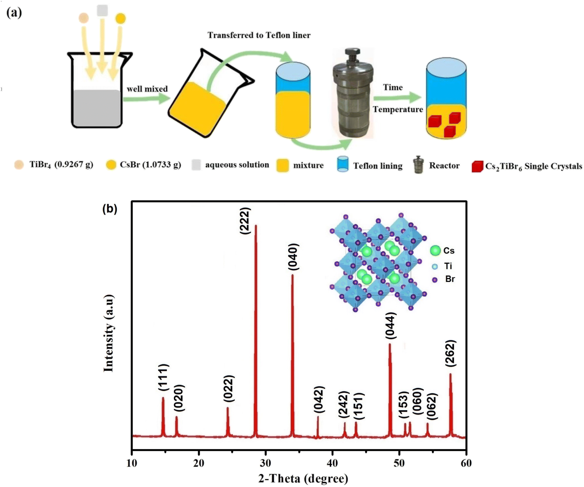
Cs2TiBr6 single crystals were prepared using the solvothermal process depicted in Fig. 1(a). This synthesis was achieved through the controlled gradual cooling method. The precursor solution underwent a controlled cooling process, transitioning from 130 °C to room temperature at a controlled rate of 0.5 °C per hour, deviating from the conventional natural cooling approach. Once it reached room temperature, the precursor solution was allowed to stabilize for a period of several days. At the conclusion of the experiment, we facilitated the growth of Cs2TiBr6 single crystals by employing a controlled, gradual solvent evaporation technique.
 |
| | Fig. 1 (a) Schematic illustration of the slow cooling method to obtain Cs2TiBr6 SCs. (b) Powder X-ray diffraction pattern of Cs2TiBr6 obtained at ambient temperature within the 2θ range of 10–60°. The inset displays the arrangement of Cs2TiBr6 in the crystal lattice. | |
2.3. Device characterization
The XRD patterns were determined by employing micro-beam XRD equipment (Bruker D8 Discover) utilizing Cu KαI radiation, with a tube voltage set at 40 kV and a current of 40 mA.
HAADF-STEM pictures and Energy Dispersive X-ray Spectroscopy (EDS) data were collected with a Cs-corrected JEOL JEM-2100 F microscope set to 200 kV. A JEOL Silicon Drift Detector (DrySD60 GV) with a sensor size of 60 mm2 was used for EDS mapping, spanning an estimated solid angle of 0.5 steradians.
The thermogravimetric analysis (TGA) was performed using a PerkinElmer Pyris 6 instrument in a closed perforated aluminum pan. The heating rates ranged from 0 to 500 °C.
The UV-Vis absorbance spectra were measured using a UV-2550 spectrometer with an integrating sphere.
The steady-state PL was measured using an Edinburgh Instruments FLS 920 PL spectrometer with a 450 nm and 5 MHz light source.
The fabrication of indium tin oxide (ITO) electrodes involved the application of pulsed laser deposition (PLD) technique on both the upper and lower surfaces of the Cs2TiBr6 single crystal. A macroscopic measurement involved the use of a copper conductor, while for microscopic measurements, the specimen was securely bonded to an alumina plate using silver paste. The assessment of macroscopic photocurrent involved the utilization of an 6517B Electrometer/High Resistance Meter Datasheet. We employed a white light-emitting diode (LED) as the illumination source for conducting photocurrent measurements in the presence of light. The incident light intensity was standardized through measurements taken under a solar simulator. Additionally, a xenon lamp sourced from Perfect Light Technology Co., Ltd. in China was utilized as an alternative light source, with a wavelength range spanning from 320 to 2500 nm.
We conducted complex impedance measurements by placing a material pellet with an 8 mm diameter and variable thickness between two copper electrodes. This analysis was carried out using a Hioki LCR Q meter (IM3536) instrument. The dielectric investigations encompassed a broad frequency range (1–107 Hz) and were conducted at various temperatures, ranging from 303 to 383 K.
3. Results and discussion
Fig. 1(b) presents the XRD pattern of Cs2TiBr6 at room temperature. All observed reflection peaks were indexed to the cubic phase with the space group Fm![[3 with combining macron]](https://www.rsc.org/images/entities/char_0033_0304.gif) m (225) at approximately 297 K. The lattice parameters of the selected unit cell, a = 10.598 (4) Å and V = 1190.34 (Å3), were refined using Celeref3 software,18,19 consistent with values reported in the literature.20 The inset of Fig. 1(b) illustrates the crystal structure of cubic Cs2TiBr6, determined using Vesta software.21
m (225) at approximately 297 K. The lattice parameters of the selected unit cell, a = 10.598 (4) Å and V = 1190.34 (Å3), were refined using Celeref3 software,18,19 consistent with values reported in the literature.20 The inset of Fig. 1(b) illustrates the crystal structure of cubic Cs2TiBr6, determined using Vesta software.21
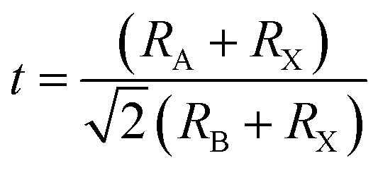
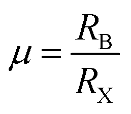
We conducted a concise theoretical assessment to evaluate the stability and structural geometry of the compound. Within this analysis, we examined the significance of the Goldschmidt tolerance factor (t) and the octahedral factor (μ) as crucial parameters for both assessing perovskite stability and investigating the formation of perovskite structures. In a recent development, Bartel and colleagues introduced a novel Tolerance factor termed ‘τ’ known for its remarkable predictive accuracy (as described in eqn (3)). These parameters, ‘t,’ ‘μ,’ and ‘τ,’ are computed using the following equations, specifically tailored for ABX3 perovskite structures:22–24
| |
 | (1) |
| |
 | (2) |
| |
 | (3) |
In this context, ‘nA’ signifies the oxidation state of element A, and it's important to note that ‘RA’ is inherently greater than ‘RB’ as per the definition. Additionally, ‘RA,’ ‘RB,’ and ‘RX’ correspond to the ionic radii of ions A, B, and X, respectively. Given the presence of two distinct B cations within double perovskite materials, ‘RB’ denotes the mean radius that encompasses both B+ and B3+ cations. As a fundamental guideline for the establishment of a stable perovskite structure, it is essential that the Goldschmidt tolerance factor ‘t,’ the tolerance factor ‘τ,’ and the octahedral factor ‘μ’ fall within specific intervals: ‘t’ should ideally range from 0.81 to 1.11, ‘τ’ should remain below 4.18, and ‘μ’ should typically fall between 0.41 and 0.90.22 We provide a summarized presentation of the three pivotal parameters, namely ‘t,’ ‘τ,’ and ‘μ,’ for Cs2TiBr6 in Table 1. Our calculations reveal that Cs2TiBr6 falls within the stable range for these ‘t,’ ‘τ,’ and ‘μ’ values.
Table 1 Goldschmidt's tolerance factor (t), octahedral factor (μ), and new tolerance factor (τ) of Cs2TiBr6
| |
Goldschmidt tolerance factor t |
New tolerance factor τ |
Octahedral factor μ |
| Cs2TiBr6 |
0.96 |
3.825 |
0.61 |
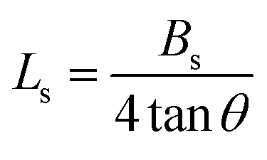
The lattice strain (Ls) in Cs2TiBr6 is assessed by analyzing the full width at half-maximum (FWHM) of individual reflections (Table 2), using the tangent formula as described in ref. 25–27;
| |
 | (4) |
Table 2 FWHM and Ls values according to all XRD reflections
| Miller indices (hkl) |
FWHM (°) |
Ls (%) |
| (111) |
0.053 |
0.074 |
| (020) |
0.058 |
0.077 |
| (022) |
0.064 |
0.085 |
| (222) |
0.081 |
0.104 |
| (040) |
0.078 |
0.101 |
| (042) |
0.022 |
0.045 |
| (242) |
0.051 |
0.074 |
| (151) |
0.047 |
0.071 |
| (044) |
0.079 |
0.108 |
| (153) |
0.029 |
0.050 |
| (060) |
0.035 |
0.062 |
| (062) |
0.048 |
0.074 |
| (262) |
0.070 |
0.098 |
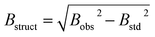
Bs quantifies structural expansion, indicating the difference in the integral profile width between a standard reference (‘std’) and the sample under investigation (‘obs’).
| |
 | (5) |
Bobs denotes the width obtained from the compound being examined, while Bstd represents the width derived from a standard compound unaffected by structural broadening effects.
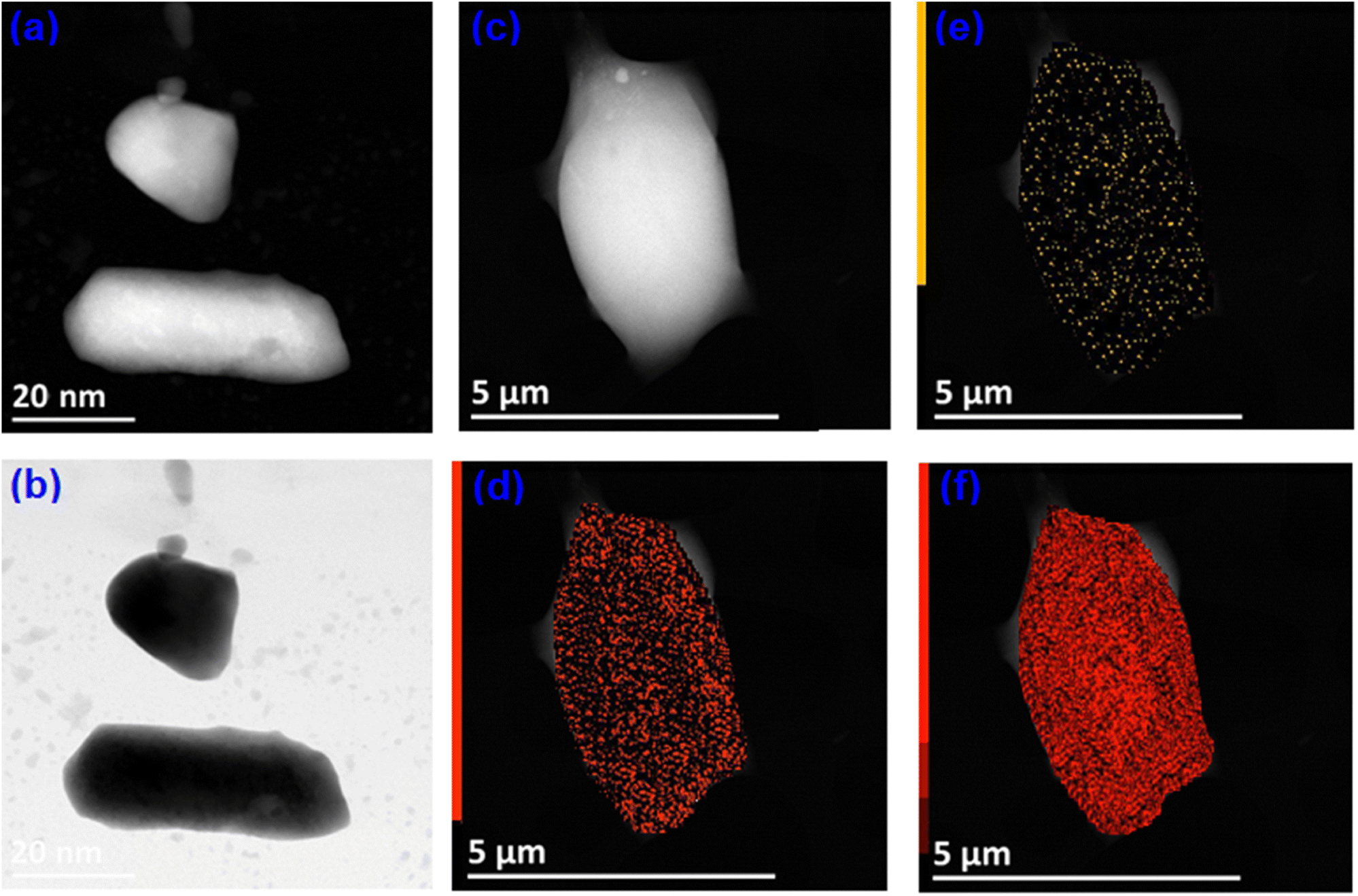
We employed a Field Emission Scanning Electron Spectroscope to analyze the morphological characteristics and particle shapes within the Cs2TiBr6 powder sample, as illustrated in Fig. 2(a) and (b). This image reveals that the predominant particle morphology is spherical and relatively small in size. Specifically, Fig. 2(a) and (b) zoom in on a single spherical particle, with a diameter measuring approximately 40 nm.
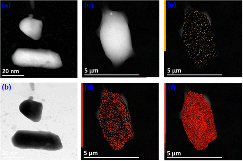 |
| | Fig. 2 (a), (b) STEM-HAADF image of Cs2TiBr6. (c)–(f) EDS mapping of Cs, Ti and Br in different colors. | |
We performed a STEM-EDS analysis (as shown in Fig. 2(c)–(f)) to confirm the elemental composition of the Cs2TiBr6 sample we prepared. The EDS mapping unequivocally reveals the presence of all the anticipated elements cesium (Cs), titanium (Ti), and bromine (Br) with no indication of any element being lost. These results provide strong evidence for the 100% purity of the synthesized Cs2TiBr6, as corroborated in Table 3.
Table 3 Elemental composition in atomic percentages
| Chemical element |
% Atomic |
| Caesium (Cs) |
21.78 |
| Titanium (Ti) |
11.03 |
| Bromine (Br) |
67.19 |
We conducted TGA on Cs2TiBr6 powder that had undergone a two-hour annealing process at 100 °C (see Fig. 3). The results indicate a lowered onset temperature, approximately at 190 °C. After reaching 450 °C, the weight stabilizes at approximately 62% of the initial mass. If we assume the decomposition of Cs2TiBr6 into CsBr and TiBr4, considering the potential evaporation of TiBr4, it would result in a final weight of around 54%. The contrast between the anticipated and actual weight reductions hints at the potential creation of an oxide compound either prior to or during the TGA assessment.
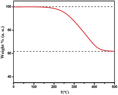 |
| | Fig. 3 TG data of Cs2TiBr6 in the temperature range of 0–500 °C. | |
Fig. 4(a) displays the absorption spectrum of Cs2TiBr6, encompassing wavelengths from 400 to 900 nm. Subsequently, we conducted a Tauc analysis28 on the absorption spectrum obtained from a single crystal of Cs2TiBr6 (Fig. 4(b)), resulting in the determination of a direct bandgap (Eg) value of 1.80 eV. The peak in the PL spectrum is found at ∼696.5 nm (1.78 eV), which is logically near to the bandgap (Fig. 4(b)). The lack of emission bands connected to defect levels suggests that the crystals in their as-grown state exhibit a limited presence of impurities and defects.29
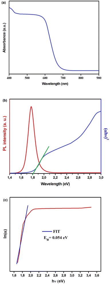 |
| | Fig. 4 (a) Absorption, (b) photoluminescence spectra and Tauc plot of Cs2TiBr6. (c) ln(α) vs. hν (eV) of Cs2TiBr6. | |
The Urbach parameter, symbolized as Eu, is associated with extended transitions occurring within the valence band as well as the localized states present in the conduction band. This parameter, grounded in empirical principles, offers valuable insights into the material's defect density. Urbach's law serves as a tool for gauging the degree of disorder within the compound by establishing an empirical connection between the absorption coefficient (α) and energy (hν), as depicted in the following equation:30
| |
 | (6) |
where
α0 is a constant.
| |
 | (7) |
In Fig. 4(c), we present a visual representation of the theoretical fitting of the natural logarithm of the absorption coefficient (ln(α)) in relation to energy (hν). The Urbach parameter was derived by taking the reciprocal of the slope of this curve. The resulting Urbach energy value determined for Cs2TiBr6 was 0.054 eV.
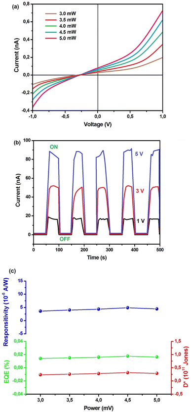
In order to explore the potential applications of Cs2TiBr6 SC in photoelectric responses, we produced a photo-detector configuration (ITO/Cs2TiBr6/ITO). Subsequently, we observed the semiconductor traits under illumination by light. Illustrated in Fig. 5(a) are the current–voltage (I–V) attributes of the device when exposed to light. As the illumination power escalates from 3 to 5 mW, the photocurrent of the device shows a progressive rise, reaching 0.73 nA. This is attributed to the correlation between the quantity of photogenerated carriers and the absorbed photon flux.31
 |
| | Fig. 5 (a) Current–voltage (I–V) curves depicting variations in light illumination powers for the investigated photodetector. (b) Temporal behavior of the device undergoing on/off switching at various bias voltages. (c) Variations in the photodetector's responsivity (R), external quantum efficiency (EQE), and specific detectivity (D*) in relation to different levels of light illumination power. The measurement of all photocurrents was conducted under simulated sunlight conditions, employing an artificial xenon lamp as the light source. | |
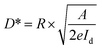
The diode-like characteristics observed in the I–V curve and the 0.22 V photovoltage can be attributed to the inherent asymmetry in the electrodes (Fig. 5(a)). Examining the current response under light on/off conditions in Fig. 5(b) demonstrates a consistently repeatable pattern across various voltage levels. This underscores the effective optical switching performance of the photodetector device.
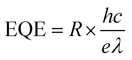
A discernible photocurrent of approximately 18 nA was observable at a modest voltage of 1 V when subjected to 5 mW light exposure, highlighting its capability to accurately detect relatively subtle signals.32,33 Expressed as a key performance metric for photodetectors, the responsivity (R) delineates the ratio of generated photocurrent to the incident light power per unit area. This parameter holds significant importance in assessing the device's effectiveness.
| |
 | (8) |
where
A and
Popt represent the effective illuminated area (electrodes made of ITO, covering an area of 3 mm
2 on each side of the Cs
2TiBr
6 SC) and the incident light power, respectively.
| | |
Iph = Iphotocurrent − Id
| (9) |
where
Id and
Iphotocurrent represent the dark current and photocurrent, respectively.
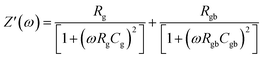
Depicted in Fig. 5(c) is the consistent relationship between incident irradiance power and responsivity. The curve exhibits stability throughout. Additionally, the performance of the photoelectric detector is evaluated using two other parameters external quantum efficiency (EQE) and specific detectivity (D*) as expressed in the subsequent equation:
| |
 | (10) |
| |
 | (11) |
The symbols in these equations retain their standard meanings and interpretations.
By utilizing eqn (10) and (11), the values for external quantum efficiency (EQE) and specific detectivity (D*) were graphically represented, as illustrated in Fig. 5(c). Within the test range, the computed values for EQE and D* exhibit stability at 0.015% and 0.25 × 10¹¹ Jones, respectively.
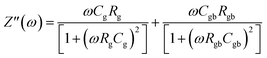
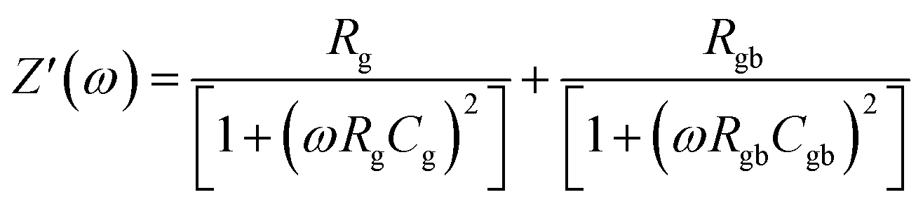
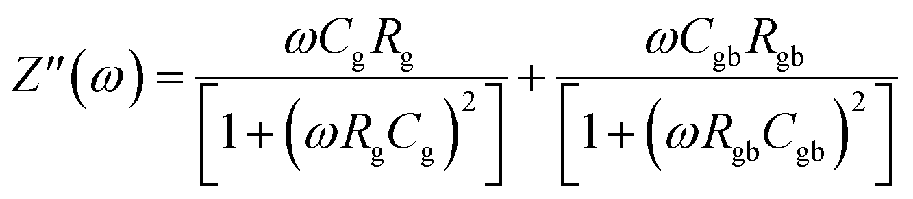
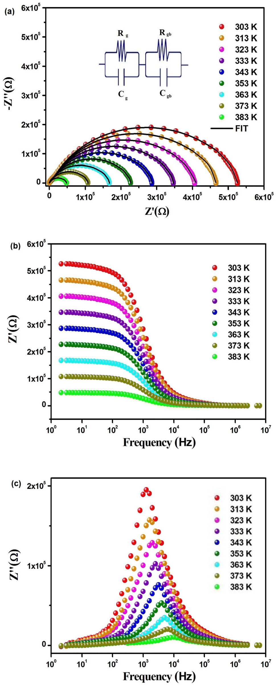
Fig. 6(a) illustrates the frequency-dependent real part of complex impedance Z′(ω) plotted against the imaginary part of impedance Z′′(ω) at various temperatures. This representation, often referred to as the Cole–Cole plot or Nyquist diagram, is a well-recognized tool in materials analysis. In the Nyquist diagram of typical dielectric materials, three discernible semicircles emerge, each corresponding to the contributions of the grain, grain boundary, and electrode–material interface towards the overall impedance of the dielectric material.34 Semicircles observed in the high-frequency range indicate the impedance contributions originating from the grain, while those appearing in the low-frequency region are linked to the involvement of the material's grain boundary. Finally, the presence of semicircles in the ultralow frequency range is attributed to the influence of the electrode–material interface.35 In Fig. 6(a), the full range of impedance spectra for the sample is presented, spanning temperatures from 303 to 383 K. These spectra reveal distinctive singular depressed semicircles, which, upon closer examination, can be seen as a composite of two successive semicircles encapsulating the overall characteristics of both grain and grain boundary. In the case of the Cs2TiBr6 perovskite, there is a complete absence of any discernible contribution from the electrode–material interface. Distinguishing between the influences of the grain and grain boundary within this single depressed semicircle proves to be a challenging task. In order to differentiate and isolate the respective contributions of the grain and grain boundary within the single semicircles, we utilize the Maxwell–Wagner equivalent circuit model.36 This model involves a parallel arrangement of multiple resistors (R) and capacitors (C). We employed the EC lab software to fit the impedance spectra acquired at various temperatures. In this scenario, the desired circuit model was achieved by interconnecting two parallel RC elements in a series configuration, as visually represented in the inset of Fig. 6(a). Additionally, as illustrated in Fig. 6(a), there is a noticeable reduction in the diameter of the semicircle the point of intersection on the real axis as the temperature increases. This reduction signifies an augmentation in DC conductivity at elevated temperatures. The formal expression for complex impedance can be articulated as follows:
| | |
Z(ω) = Z′(ω) + jZ′′'(ω)
| (12) |
where
Z′(
ω) and
Z′′(
ω) represent their conventional expressions as previously described,
| |
 | (13) |
| |
 | (14) |
Here,
Rg signifies the resistance associated with the grain,
Cg denotes the capacitance linked to the grain,
Rgb represents the resistance attributed to the grain boundary, and
Cgb stands for the capacitance associated with the grain boundary.
Table 4 encompasses all the recorded values of
R and
C for the sample across different temperature conditions.
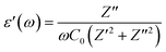
Fig. 6(b) showcases the changes in the frequency-dependent
Z′(
ω) within the temperature range of 303 to 383 K. The observed behavior exhibits a sigmoidal-type variation with frequency. We note that the real component of impedance,
Z′(
ω), exhibits a greater magnitude in the low-frequency domain. As the frequency and temperature increase, the values of
Z′(
ω) decline, in accordance with the negative temperature coefficient of resistance. This, in turn, leads to an elevation in AC conductivity with rising temperature.
36 Over time, the influence of grain boundaries on the overall impedance diminishes in the higher frequency range, given that
Z′(
ω) exhibits a declining trend with increasing frequency and temperature. In the high-frequency region, no discernible alteration of
Z′(
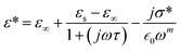
ω) is noted with changes in temperature, leading to their convergence. This behavior can be attributed to the possible release of space charges and a concurrent decrease in barrier properties, ultimately contributing to the enhancement of AC conductivity. The evolution of the imaginary component of impedance,
Z′′(
ω), as a function of frequency can be regarded as a representation of the loss spectrum. The frequency-dependent behavior of
Z′′(
ω) exhibits distinctive relaxation peaks, which exhibit a remarkable dependence on temperature, as depicted in
Fig. 6(c). Essentially, when the external field frequency aligns with the localized hopping electron frequency, it results in the emergence of relaxation peaks. These observed relaxation peaks are notably broader than the theoretical Debye curve, indicating that Cs
2TiBr
6 demonstrates a non-Debye type of relaxation. The breadth of the peak corresponds to the relaxation time, and it is apparent that the width of the relaxation peak is directly proportional to the temperature. Consequently, as the temperature increases, the width of the relaxation peak progressively expands.
16,17
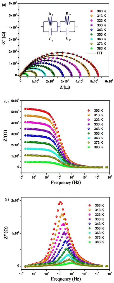 |
| | Fig. 6 (a) Adjusted Cole–Cole diagrams for Cs2TiBr6 at various temperatures, with corresponding equivalent circuits illustrated in the inset. Temperature-dependent variation of (b) Z′(f) and (c) Z′′(f). | |
Table 4 Circuit components (R and c) for Cs2TiBr6 compound across varied temperatures
| Temperature (K) |
Rg (kΩ) |
Cg (nF) |
Rgb (kΩ) |
Cgb (pF) |
| 303 |
201.62 |
1.03 |
520.17 |
2.20 |
| 313 |
186.58 |
1.27 |
469.53 |
11.46 |
| 323 |
168.14 |
1.55 |
402.25 |
17.04 |
| 333 |
144.35 |
1.73 |
348.05 |
25.58 |
| 343 |
117.88 |
1.92 |
394.71 |
31.35 |
| 353 |
98.45 |
2.12 |
331.65 |
37.98 |
| 363 |
70.93 |
2.36 |
260.35 |
46.21 |
| 373 |
47.55 |
2.51 |
180.68 |
52.69 |
| 383 |
25.11 |
2.78 |
112.48 |
63.50 |
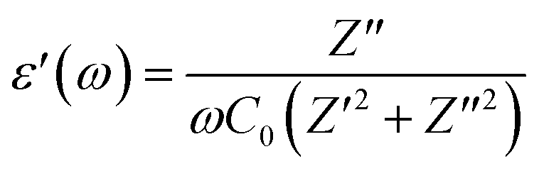
With an external oscillating electric field in a given frequency domain, the dielectric behavior of Cs2TiBr6 can be characterized by a complex permittivity. The frequency-dependent complex dielectric permittivity can be expressed by eqn (15):
| | |
ε(ω) = ε′(ω) + jε′′(ω)
| (15) |
where the real part
ε′(
ω) defines the charge storing capacity and the imaginary part
ε′′(
ω) indicates the energy loss within the material.
36 ε′(
ω) and
ε′′(
ω) have been determined using
eqn (16) and
(17):
| |
 | (16) |
| |
 | (17) |
where
ω = 2π
f is the angular frequency and
C0 =
ε0A/
t (in which
ε0 is the free space permittivity, and
A and
t are the cross-sectional area and thickness of the pellet, respectively). In the case of any semiconducting material, analysis of the relaxation process through the frequency variation plot is a little bit difficult due to the presence of DC conductivity which obscures any relaxation process.
16 Fig. 7(a) depicts the variation of
ε′(
ω) with frequency and
Fig. 7(b) shows the variation of dielectric loss
ε′′(
ω) with frequency. Both of them decrease at a faster rate with frequency in the low-frequency zone and a slow decreasing rate in the high-frequency zone, indicating frequency independence for both of
ε′(
ω) and
ε′′(
ω). Koop's phenomenological theory based on the Maxwell–Wagner model can be used to demonstrate the frequency-dependent behavior of
ε′(
ω) and
ε′′(
ω).
37–39 According to this theory, the material can be assumed as an inhomogeneous medium consisting of a number of grains that are separated by poorly conducting grain boundaries or potential barriers. The electrons, influenced by the applied field, move toward grain boundary by hopping method. Now, if the resistance is high enough at the grain boundary, then the electrons pile up at the grain boundaries and produce polarization. But with the increase of frequency, they cannot follow the alternation of applied field and move in reverse direction,
i.e., decreases in polarization.
37–39 The ionic polarization within the materials arises due to the separation of negative [TiBr
6]
2−, and positive Cs
+ charge centers. Higher values of
ε′(
ω) at low frequencies may be attributed to the contribution of ionic polarization within the materials.
 |
| | Fig. 7 Temperature-dependent of (a) ε′(f) and (b) ε′′(f) for Cs2TiBr6. | |
To investigate the fluctuations in the dielectric constant and dielectric loss concerning different temperature levels, we have utilized an adapted version of the Cole–Cole model, incorporating a direct current (DC) conductivity and a corrective component, within a repertoire of commonly adopted theoretical frameworks. According to this tailored Cole–Cole model, the complex permittivity can be formulated as follows:40
| |
 | (18) |
| |
 | (19) |
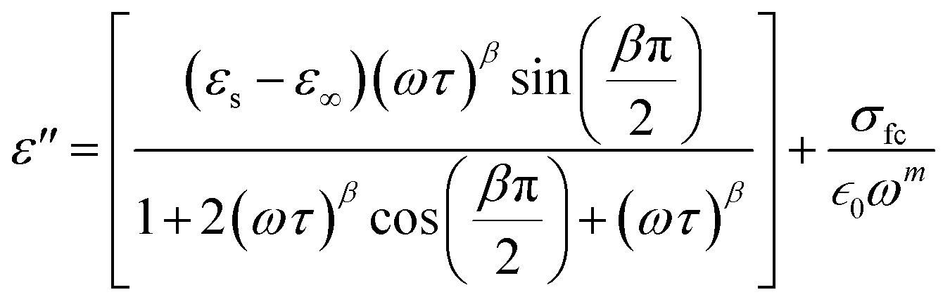
In this context, σ* denotes the combination of conductivity attributed to space charge carriers (σsp) and that arising from free charge carriers (σfc). εs signifies the lower frequency threshold for permittivity, while ε∞ denotes its upper frequency threshold. The symbol m is recognized as the frequency exponent, and β corresponds to the adjusted Cole–Cole parameter, constrained within the range of 0 to 1. τ stands for the relaxation time. Furthermore, ε′ and ε′′ can be expressed as eqn (20) and (21):
| |
 | (20) |
| |
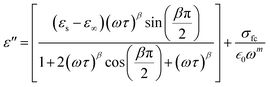 | (21) |
The experimental measurements of ε′ and ε′′ have been subjected to fitting using the modified Cole–Cole equation. The resulting outcomes encompass the determination of various parameters, including β, m, σsp, σfc, and τ, which have been tabulated in Table 5. Analysis of the data presented in Table 5 reveals that as the temperature rises, both space charge conductivity (σsp) and free charge conductivity (σfc) exhibit an upward trend. Moreover, the observed range of β values between 0 and 1 provides additional evidence supporting the non-Debye nature of the system. Additionally, it is noteworthy that the relaxation time decreases as the temperature increases.
Table 5 .Determination of β, m, σsp, σfc and τ parameters through modified Cole–Cole model fitting
| Parameter |
Temperature |
| 303 K |
313 K |
323 K |
333 K |
343 K |
453 K |
363 K |
373 K |
383 K |
| τ (10−3) |
17.54 |
14.28 |
11.04 |
7.39 |
5.11 |
2.72 |
0.68 |
0.09 |
0.05 |
| β |
0.758 |
0.624 |
0.725 |
0.632 |
0.789 |
0.804 |
0.714 |
0.803 |
0.698 |
| ? |
0.706 |
0.738 |
0.770 |
0.804 |
0.836 |
0.872 |
0.889 |
0.909 |
0.924 |
| σsp (10−3) |
0.051 |
0.122 |
0.458 |
0.832 |
2.355 |
4.851 |
7.059 |
9.480 |
12.976 |
| σfc (10−2) |
0.0276 |
0.0589 |
1.142 |
3.657 |
5.489 |
8.026 |
9.974 |
13.542 |
15.735 |
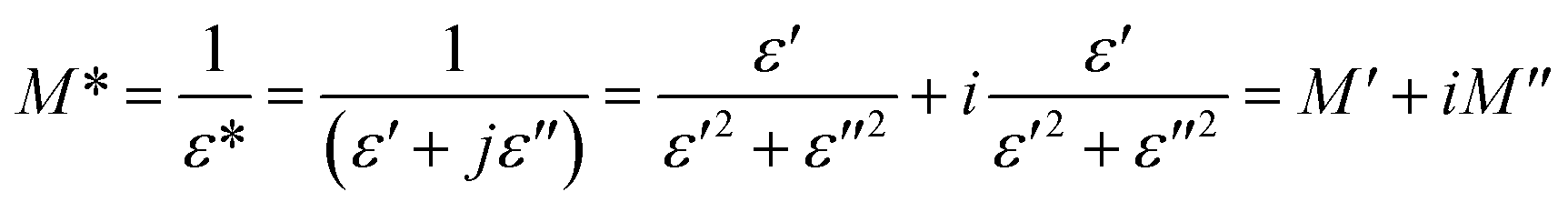
The study of dielectric relaxation in Cs2TiBr6 perovskite has been effectively conducted through modulus analysis. The dielectric modulus can be expressed as follows:41
| |
 | (22) |
where
M′(
ω) and
M′′(
ω) present the real and imaginary parts of electric modulus, respectively.
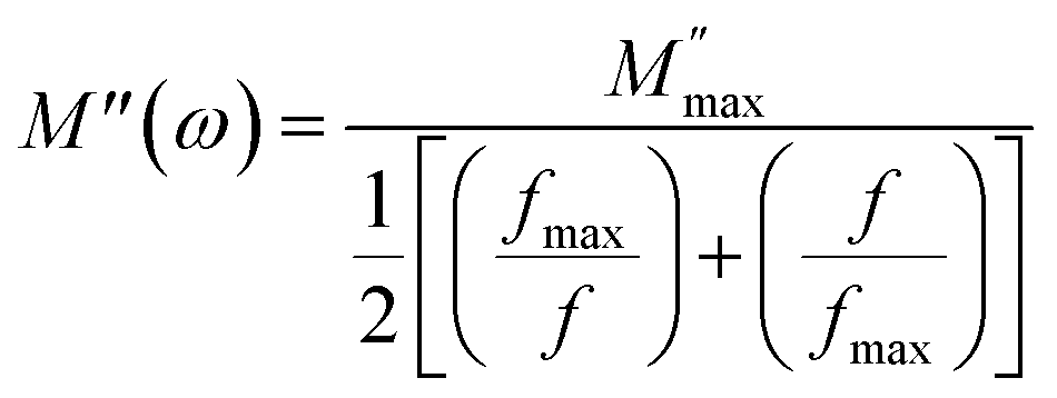
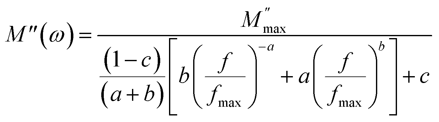
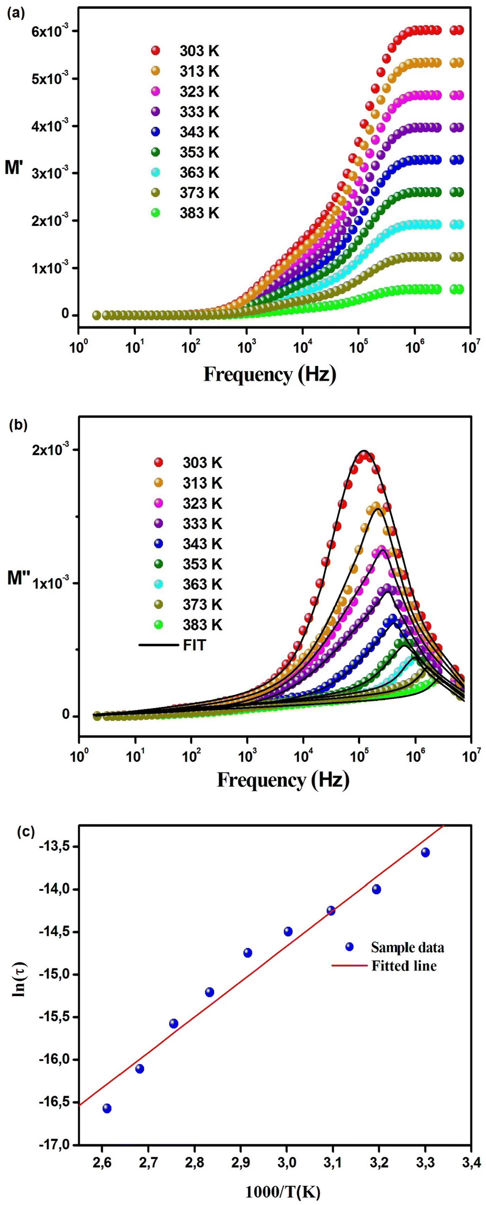
In Fig. 8(a), the real part of the electric modulus spectra is presented as a function of frequency across a range of temperatures. The behavior of M′ with respect to the frequency of Cs2TiBr6 reveals that, for all temperatures, M′ assumes a remarkably low value, approaching zero, in the low-frequency region. The presence of a low M′ value in the low-frequency range and the sigmoidal shape of M′ can be attributed to the extensive mobility of charge carriers in the conduction mechanism and the minimal impact of electrode polarization. A subtle shift in the M′ peak is observed within the high-frequency range as the temperature increases. Fig. 8(b) illustrates the frequency-dependent changes in the imaginary part of the electric modulus, denoted as M′′, at various temperatures. At a specific temperature, M′′ reaches its highest value, resulting in the emergence of a peak at a particular frequency, which corresponds to the relaxation frequency. In the low-frequency range, no discernible peak is detected, whereas a conspicuous, broad, and substantial peak becomes evident within the high-frequency domain. In the lower frequency region, there is a noticeable capability for charge carriers to move freely over extended distances, indicating successful charge hopping between adjacent sites. Conversely, within the high-frequency range, charge carriers experience confinement within their respective potential wells, leading to restricted motion confined to the short range of these wells. Consequently, the appearance of a peak offers valuable insights into the transition from the mobility of charge carriers spanning long distances to the confinement of their mobility within shorter ranges. These M′′ peaks tend to shift towards higher frequency regions as temperature increases, a phenomenon that can be attributed to the hopping mechanism. The asymmetrical characteristics displayed by the M′′ peaks signify the non-Debye nature of the sample's response. To account for the asymmetry observed in the peaks within the imaginary component of the electric modulus, Bergman introduced a comprehensive function in 2000. This function incorporates a modified Kohlrausch–Williams–Watts (KWW) function with separate shape parameters for the low and high-frequency regions. Additionally, it includes a smoothing parameter that applies to the M′′ spectra, as detailed in eqn (23).17
| |
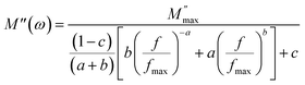 | (23) |
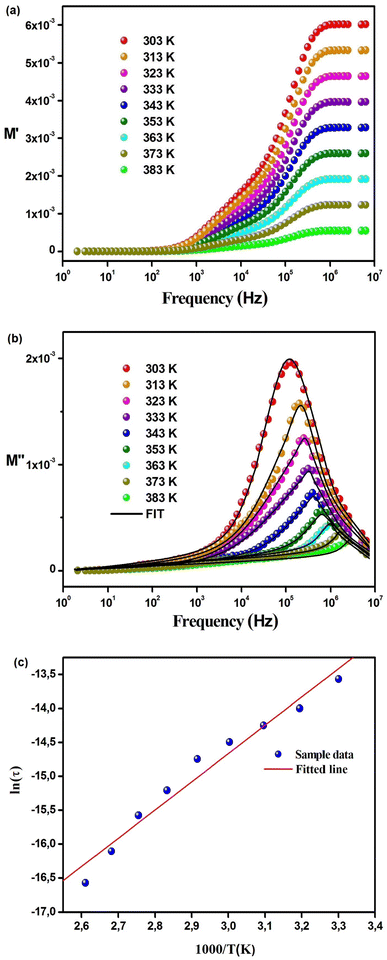 |
| | Fig. 8 Temperature-dependent changes in (a) M′(f) and (b) M′′(f) for Cs2TiBr6. (c) Arrhenius plot of  . . | |
In this context, we define  as the peak value observed in the imaginary component of the electric modulus, and we designate the corresponding frequency as fmax. Parameters a and b are employed as independent shape parameters for the low and high-frequency regions, respectively, while c is introduced as the smoothing parameter. It's worth noting that when both a and b are set to 1, and c is equal to 0, eqn (23) simplifies into eqn (24), which characterizes the ideal Debye-type behavior. The symmetrical nature of M′′ spectra, as a function of frequency, is a hallmark of the ideal Debye-type response. Fig. 8(b) showcases the fitting of the modified KWW function through the solid line, with details regarding the shape parameters for different temperatures conveniently summarized in Table 6. The temperature-dependent analysis reveals that ‘a’ and ‘b’ values steadily increase as the temperature elevates, converging toward unity. This trend suggests that as temperature rises, M′′(ω) tends to approach an ideal Debye-type response.16
| |
 | (24) |
Table 6 The values for the parameters a and b were determined through a fitting process, aligning M′′(ω) with the modified KWW function
| Temperature (K) |
a |
b |
| 303 |
0.556 |
0.463 |
| 313 |
0.579 |
0.486 |
| 323 |
0.603 |
0.568 |
| 333 |
0.634 |
0.603 |
| 343 |
0.662 |
0.669 |
| 353 |
0.685 |
0.699 |
| 363 |
0.749 |
0.720 |
| 373 |
0.790 |
0.749 |
| 383 |
0.822 |
0.771 |
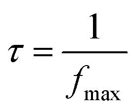
The calculation of the relaxation time is based on the equation presented in eqn (25).
| |
 | (25) |
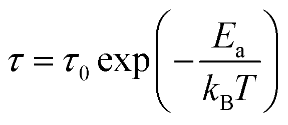
To estimate the average activation energy of charge carriers, one can apply the Arrhenius equation, which is provided in eqn (26).
| |
 | (26) |
By examining the ln(τ) versus 1000/T plot, as illustrated in Fig. 8(c), we can calculate the activation energy. In this analysis, the determined activation energy amounts to 0.307 eV. This finding provides additional evidence supporting the conduction mechanism in Cs2TiBr6 as being driven by thermally stimulated charge carriers.
In Fig. 9(a), we observe the changes in temperature-dependent AC conductivity as a function of frequency. The determination of AC electrical conductivity involves the application of the following formula: σac = ωε′ε0![[thin space (1/6-em)]](https://www.rsc.org/images/entities/char_2009.gif) tanδ, where ε0 represents the permittivity of free space. In our study, the conductivity in the low-frequency region is primarily influenced by DC conductivity, whereas in the high-frequency region, AC conductivity becomes the dominant factor. The coexistence of frequency-independent and temperature-dependent DC conductivity contributes to the flattening of the curves observed in the low-frequency region.13,14 Nonetheless, with the increase in frequency, the electrical conductivity profiles experience considerable augmentation, signifying a marked frequency dispersion phenomenon. This phenomenon primarily stems from the substantial influence of AC conductivity. The frequency at which this conductivity transition takes place is termed “frequency hopping” (ωP). Notably, as the temperature increases, this ωP parameter shifts towards higher frequencies in the spectrum. The concept known as the jump relaxation model (JRM), originally formulated by Funke, provides insights into the observed frequency-dependent AC conductivity and the concurrent frequency-independent DC conductivity.42 This theoretical framework suggests that at lower frequencies, ions can effectively undergo hopping transitions to neighboring sites. The DC conductivity arises from sustained availability of successful jumps at lower frequencies, leading to long-range translational ion motion. In contrast, at higher frequencies, the conductivity dynamics involve a combination of both successful and unsuccessful hopping behaviors, contributing to the observed behavior.13 Unsuccessful ion hopping arises when the ion attempting to jump retraces its path, effectively moving forward, then backward, and forward once more to its initial location. Conversely, successful hopping entails the excited jumping ion relocating to a new site and attaining stability in this fresh position, while the neighboring ions relax in concert with the stationary ion. In the high-frequency domain, an increase in the ratio between unsuccessful and successful ion hopping is evident, leading to dispersive conductivity in this particular range. The recorded electrical conductivity can be attributed to Jonscher's power law, commonly referred to as the Universal Dielectric Response (UDR) model, which was originally formulated by Jonscher. This model is expressed by the next equation:17
tanδ, where ε0 represents the permittivity of free space. In our study, the conductivity in the low-frequency region is primarily influenced by DC conductivity, whereas in the high-frequency region, AC conductivity becomes the dominant factor. The coexistence of frequency-independent and temperature-dependent DC conductivity contributes to the flattening of the curves observed in the low-frequency region.13,14 Nonetheless, with the increase in frequency, the electrical conductivity profiles experience considerable augmentation, signifying a marked frequency dispersion phenomenon. This phenomenon primarily stems from the substantial influence of AC conductivity. The frequency at which this conductivity transition takes place is termed “frequency hopping” (ωP). Notably, as the temperature increases, this ωP parameter shifts towards higher frequencies in the spectrum. The concept known as the jump relaxation model (JRM), originally formulated by Funke, provides insights into the observed frequency-dependent AC conductivity and the concurrent frequency-independent DC conductivity.42 This theoretical framework suggests that at lower frequencies, ions can effectively undergo hopping transitions to neighboring sites. The DC conductivity arises from sustained availability of successful jumps at lower frequencies, leading to long-range translational ion motion. In contrast, at higher frequencies, the conductivity dynamics involve a combination of both successful and unsuccessful hopping behaviors, contributing to the observed behavior.13 Unsuccessful ion hopping arises when the ion attempting to jump retraces its path, effectively moving forward, then backward, and forward once more to its initial location. Conversely, successful hopping entails the excited jumping ion relocating to a new site and attaining stability in this fresh position, while the neighboring ions relax in concert with the stationary ion. In the high-frequency domain, an increase in the ratio between unsuccessful and successful ion hopping is evident, leading to dispersive conductivity in this particular range. The recorded electrical conductivity can be attributed to Jonscher's power law, commonly referred to as the Universal Dielectric Response (UDR) model, which was originally formulated by Jonscher. This model is expressed by the next equation:17
where
σAC and
σDC pertain to the alternating current (AC) and direct current (DC) components contributing to the overall conductivity, respectively.
σ0 represents a fixed constant, while
S is characterized as the frequency exponent, with its range confined between 0 and 1. Fundamentally,
S reflects the interplay between charge carriers and the lattice structure within the sample.
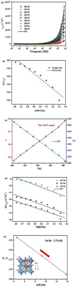 |
| | Fig. 9 (a) Variation of σac(f) at different temperatures. (b) σac vs. 1000/T plot of Cs2TiBr6. (c) Variation of s and (1 − s) with temperature. (d) The temperature dependency of the ln(σac) at various frequencies. (e) Frequency-dependent of Rω. | |
The frequency-dependent conductivity data for the sample has been utilized to perform a fitting procedure employing the Universal Dielectric Response (UDR) model. This process is illustrated in Fig. 9(a).
Nonetheless, employing the UDR model, we have computed σDC values at different temperatures. This calculation involved non-linear curve fitting applied to the σAC data. By constructing a plot correlating ln σDC with 1000/T (as depicted in Fig. 9(b)), we have determined the activation energy (Ea) for Cs2TiBr6 using the Arrhenius equation:
| |
 | (28) |
The resulting activation energy for Cs2TiBr6, which closely aligns with the value obtained from the M′′ spectra, stands at 0.294 eV.
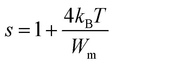
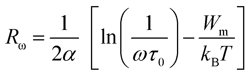
The assessment of s(T), with its capability to identify the model type, constitutes a valuable approach for probing the AC conduction mechanism inherent in the material.14 Following the NSPT model, the exponent s shows an elevation as temperature increases, signifying the dominance of small polaron hopping mechanisms within the compound (Fig. 9(c)).16 Specifically, Cs2TiBr6 contains negatively charged [TiBr6]2− ions within the presence of Cs+ ions. However, these charge centers do not align perfectly, resulting in the material's partially polar characteristics. The formation of a polaron occurs when the localized charge approaches the compound and subsequently transitions to the closest neighboring positions. The polaron exhibits two possible behaviors upon its movement: it can stabilize in its current position, termed a “successful hop,” or it may reverse its direction and aim for a partially relaxed state, referred to as an “unsuccessful hop.” Successful polaron hopping results in the emergence of non-dispersive AC conductivity behavior, particularly at low frequencies.14 However, as the hopping frequency increases, a greater number of hops fail to succeed. Consequently, higher frequencies lead to dispersive conductivity. This behavior is often linked to lattice distortion, a factor typically overlooked in the quantum mechanical electron tunneling process observed in most inorganic halide perovskite materials.16 Polarons, upon their creation through the introduction of a charge carrier to a site, are responsible for inducing substantial local lattice distortions. These distortions, associated with small polarons, exhibit a non-overlapping nature due to their spatial confinement. The AC conductivity observed at elevated temperatures can be attributed to the tunneling behavior of polarons or carriers that are confined within structural defects.13 Calculating the exponent “s” in the NSPT model involves using the next equation:17
| |
 | (29) |
To determine the value of Wm, which is approximately 0.09 eV according to eqn (29), curve fitting is employed, as illustrated in Fig. 9(c). Given that small polarons possess confined cloud distortions that do not overlap, the activation energy associated with polaron transfer (Wm) remains unaltered by variations in intersite separation. The expression for AC conductivity within the NSPT model is provided by eqn (26).
| |
 | (30) |
where
| |
 | (31) |
In this equation, the parameter α−1 represents the spatial span of the polaron, N(EF) stands for the density of states in proximity to the Fermi level, and Rω is indicative of the tunneling distance.
To validate the suitability of the fit with respect to experimental data, we present the temperature-dependent ln(σAC) at various frequencies in Fig. 9(d), revealing a strong agreement between the two. Table 7 presents the various parameters obtained for the NSPT model. These N(EF) values, indicative of localized states, are deemed adequate.17 Table 7 visually depicts the frequency-dependent variations in the parameters α and N(EF). The upward trends observed in both α and N(EF) with increasing frequency are consistent with prior research findings.14 Table 7 provides an overview of the Rω values, as elucidated through eqn (30). This relationship between Rω and frequency is graphically represented in Fig. 9(e). It's worth noting that the tunneling distances align closely with the interatomic spacing for Cs–Br (∼3.74 Å).43 Additionally, with the increase in frequency, the tunneling distance experiences a more pronounced decrease. This observation suggests a shift of charge carriers from long-distance tunneling to short-distance tunneling. This phenomenon could account for the increase in N(EF) (approximately 1021 eV−1 cm−3) as the frequency rises.13 The proximity of the Cs–Br distances (∼3.74 Å) to the values of Rω (ranging from 3.695 to 3.733 Å) suggests that the AC conductivity is facilitated by the mobility of Cs+ ions within the compound, facilitating the motion of small polarons.
Table 7 Variation of AC conductivity parameters across different frequencies within the NSPT model
| Frequency (Hz) |
α (Å−1) |
N(EF) (eV−1 cm−3) |
Rω (Å) |
| 102 |
0.79 |
9.87 × 10²⁰ |
3.733 |
| 104 |
0.84 |
2.54 × 10²¹ |
3.714 |
| 106 |
0.88 |
5.06 × 10²¹ |
3.695 |
4. Conclusions
To provide a concise overview, we have employed a controlled gradual cooling method to synthesize Cs2TiBr6 and subsequently conducted a thorough examination of its structural, optical, and extensive dielectric properties. The utilization of XRD analysis has unequivocally verified the successful generation of polycrystalline Cs2TiBr6. The examination of morphology reveals the existence of nanoparticles measuring approximately 40 nanometers in size. Cs2TiBr6 demonstrates outstanding macroscopic photodetection capabilities. The perovskite under investigation exhibits an intriguing set of properties, characterized by a notably high dielectric constant in conjunction with minimal dielectric loss when exposed to high-frequency conditions. The perovskite's high dielectric constant enhances charge separation in solar cells, improving energy conversion. Its minimal dielectric loss under high-frequency conditions ensures stable electrical properties, reducing energy dissipation for consistent performance. These properties collectively make this material promising for efficient and reliable application in solar cells. Our analytical approach, centered around the utilization of a modified Cole–Cole plot, enables us to effectively quantify two distinct forms of conductivity: space charge conductivity and free charge conductivity. Intriguingly, as the temperature escalates, both of these conductivity components exhibit a noticeable augmentation in their respective magnitudes. The investigation into AC conductivity has been conducted extensively, with a specific emphasis on elucidating the NSPT conduction mechanism. This comprehensive study not only imparts a thorough understanding of the material's behavior but also highlights its potential suitability for various practical applications. Furthermore, a meticulous analysis of dielectric properties has been undertaken, offering valuable insights into the distinct roles played by grain and grain boundary components in shaping the overall impedance characteristics. The assessment of the electric modulus curve reveals its asymmetrical nature, which necessitates an examination through the KWW equation. It is worth noting that the departure from Debye-type behavior in the imaginary part of the electric modulus progressively diminishes with increasing temperature. The determination of activation energy has been performed using data obtained from both the modulus spectra and DC conductivity measurements. The remarkably close values of activation energy indicate a striking similarity between the relaxation behavior and the conduction mechanism within the material. The straightforwardness of its structure and the simplicity of the fabrication process may position this material as an appealing candidate for the development of multilayered energy harvesting devices. The deduced advantageous energy bandgap, the determined dielectric constant, the assessed relaxation time, and most significantly, the measured conductivity collectively indicate the potential of this material as a novel and promising perovskite, suitable for utilization in energy harvesting systems.
Conflicts of interest
There are no conflicts to declare.
References
- T. A. S. Carvalho, L. F. Magalhães, C. I. D. L. Santos, T. A. Z. Freitas, B. R. De Carvalho Vale, A. F. V. Da Fonseca and M. A. Schiavon, Lead-Free Metal Halide Perovskite Nanocrystals: From Fundamentals to Applications, Chem.–Eur. J., 2022, 29(4), e202202518, DOI:10.1002/chem.202202518.
- J. Nie, B. Zhou, S. Fang, Y. Wang, Y. Wang, B. Tian, H. Hu, H. Zhong, H. Li and Y. Shi, Chemical Doping of Lead-Free Metal-Halide-Perovskite Related Materials for Efficient White-Light Photoluminescence, Mater. Today Phys., 2023, 31, 100992, DOI:10.1016/j.mtphys.2023.100992.
- M. Morana, W. Kaiser, R. Chiara, B. Albini, D. Meggiolaro, E. Mosconi, P. Galinetto, F. De Angelis and L. Malavasi, Origin of Broad Emission Induced by Rigid Aromatic Ditopic Cations in Low-Dimensional Metal Halide Perovskites, J. Phys. Chem. Lett., 2023, 14(35), 7860–7868, DOI:10.1021/acs.jpclett.3c01872.
- Q. Yang, H. Wei, G. Liu, J. Huang, X. Li and G. Cai, Recent Developments of Lead-Free Halide-Perovskite Cs3Cu2X5 (X = Cl, Br, I): Synthesis, Modifications, and Applications, Mater. Today Phys., 2023, 36, 101143, DOI:10.1016/j.mtphys.2023.101143.
- J. Arteaga, V. L. Cherrette, J. Z. Zhang and S. Ghosh, Complex Dependence of Optoelectronic Properties of Metal Halide Perovskite Thin Films on Quantum Dot Decoration Layers, J. Phys. Chem. C, 2023, 127(36), 17836–17842, DOI:10.1021/acs.jpcc.3c03832.
- S. A. Khan, N. Z. Khan, M. Sohail, M. Runowski, X. Xu and S. Agathopoulos, Recent Developments of Lead-Free Halide-Perovskite Nanocrystals: Synthesis Strategies, Stability, Challenges, and Potential in Optoelectronic Applications, Mater. Today Phys., 2023, 34, 101079, DOI:10.1016/j.mtphys.2023.101079.
- S. Martani, Y. Zhou, I. Poli, E. Aktas, D. Meggiolaro, J. Jiménez-López, E. L. Wong, L. Gregori, M. Prato, D. Di Girolamo, A. Abate, F. De Angelis and A. Petrozza, Defect Engineering to Achieve Photostable Wide Bandgap Metal Halide Perovskites, ACS Energy Lett., 2023, 8(6), 2801–2808, DOI:10.1021/acsenergylett.3c00610.
- M. Ju, M. Chen, Y. Zhou, H. F. Garcés, J. Dai, L. Ma, N. P. Padture and X. C. Zeng, Earth-Abundant Nontoxic Titanium(IV)-Based Vacancy-Ordered Double Perovskite Halides with Tunable 1.0 to 1.8 EV Bandgaps for Photovoltaic Applications, ACS Energy Lett., 2018, 3(2), 297–304, DOI:10.1021/acsenergylett.7b01167.
- M. Chen, M. Ju, A. D. Carl, Y. Zong, R. L. Grimm, J. Gu, X. C. Zeng, Y. Zhou and N. P. Padture, Cesium Titanium(IV) Bromide Thin Films Based Stable Lead-Free Perovskite Solar Cells, Joule, 2018, 2(3), 558–570, DOI:10.1016/j.joule.2018.01.009.
- G. K. Grandhi, A. Matuhina, M. Liu, S. Annurakshita, H. Ali-Löytty, G. Bautista and P. Vivo, Lead-Free Cesium Titanium Bromide Double Perovskite Nanocrystals, Nanomaterials, 2021, 11(6), 1458, DOI:10.3390/nano11061458.
- D. Kong, D. Cheng, X. Wang, K. Zhang, H. Wang, K. Liu, H. Li, X. Sheng and L. Yin, Solution Processed Lead-Free Cesium Titanium Halide Perovskites and Their Structural, Thermal and Optical Characteristics, J. Mater. Chem. C, 2020, 8(5), 1591–1597, 10.1039/c9tc05711k.
- J. Euvrard, X. Wang, T. Li, Y. Yan and D. B. Mitzi, Is Cs2TiBr6 a Promising Pb-Free Perovskite for Solar Energy Applications?, J. Mater. Chem. A, 2020, 8(7), 4049–4054, 10.1039/c9ta13870f.
- M. B. Bechir, A. Almeshal and M. H. Dhaou, Structural Evolution, Dielectric Relaxation, and Charge Transport Characteristics of Formamidinium Lead Iodide (FAPbI3) Perovskite, Mater. Res. Bull., 2023, 157, 112012, DOI:10.1016/j.materresbull.2022.112012.
- I. Romdhane, M. B. Bechir and M. H. Dhaou, Impedance Spectroscopic Study of Charge Transport and Relaxation Mechanism in the Lead-Free Hybrid Perovskite CH3NH3CuCl3, Phys. E, 2022, 136, 115008, DOI:10.1016/j.physe.2021.115008.
- M. Ben Bechir and A. Ben Rhaiem, Structural Phase Transition, Vibrational Analysis, Ionic Conductivity and Conduction Mechanism Studies in an Organic-Inorganic Hybrid Crystal: [N(CH3)3H]2CdCl4, J. Solid State Chem., 2021, 296, 122021, DOI:10.1016/j.jssc.2021.122021.
- M. Ben Bechir and M. Houcine Dhaou, Study of Charge Transfer Mechanism and Dielectric Relaxation of CsCuCl3 Perovskite Nanoparticles, Mater. Res. Bull., 2021, 144, 111473, DOI:10.1016/j.materresbull.2021.111473.
- M. B. Bechir and M. H. Dhaou, Study of charge transfer mechanism and dielectric relaxation of all-inorganic perovskite CsSnCl3, RSC Adv., 2021, 11(35), 21767–21780, 10.1039/d1ra02457d.
- M. Ben Bechir and A. Ben Rhaiem, The sodium-ion battery: Study of alternative current conduction mechanisms on the Na3PO4 - based solid electrolyte, Phys. E, 2020, 120, 114032, DOI:10.1016/j.physe.2020.114032.
- K. Karoui, M. B. Bechir, A. Bulou, K. Guidara and A. B. Rhaiem, [N(CH3)3H]2CuCl4: ab initio calculations and characterization of phase transitions by Raman spectroscopy, J. Mol. Struct., 2016, 1114, 161–170, DOI:10.1016/j.molstruc.2016.02.031.
- J. Euvrard, X. Wang, T. Li, Y. Yan and D. B. Mitzi, Is Cs2TiBr6 a Promising Pb-Free Perovskite for Solar Energy Applications?, J. Mater. Chem. A, 2020, 8(7), 4049–4054, 10.1039/c9ta13870f.
- M. B. Bechir and M. H. Dhaou, Lead-Free Double Perovskite Cs2MBiCl6 (M = Ag, Cu): Insights into the Optical, Dielectric, and Charge Transfer Properties, RSC Adv., 2023, 13(26), 17750–17764, 10.1039/d3ra02731g.
- C. Li, X. Lu, W. Ding, L. Feng, Y. Gao and Z. Guo, Formability of ABX3 (X = F, Cl, Br, I) Halide Perovskites, Acta Crystallogr., 2008, 64(6), 702–707, DOI:10.1107/s0108768108032734.
- C. J. Bartel, C. Sutton, B. R. Goldsmith, R. Ouyang, C. B. Musgrave, L. M. Ghiringhelli and M. Scheffler, New Tolerance Factor to Predict the Stability of Perovskite Oxides and Halides, Sci. Adv., 2019, 5(2), eaav0693, DOI:10.1126/sciadv.aav0693.
- F. Ji, G. Boschloo, F. Wang and F. Gao, Challenges and Progress in Lead-Free Halide Double Perovskite Solar Cells, Sol. RRL, 2023, 7(6), 2201112, DOI:10.1002/solr.202201112.
- K. Fatema, M. T. Ahmed, Md. K. Hossain and F. Ahmed, Structural and Morphological Properties of Single and Mixed Halide PB-Based Perovskites, Adv. Condens. Matter Phys., 2022, 2022, 1–7, DOI:10.1155/2022/6001569.
- S. Amari, J.-M. Verilhac, E. G. D'Aillon, A. Ibanez and J. Zaccaro, Optimization of the Growth Conditions for High Quality CH3NH3PbBr3 Hybrid Perovskite Single Crystals, Cryst. Growth Des., 2020, 20(3), 1665–1672, DOI:10.1021/acs.cgd.9b01429.
- T. W. Jones, A. Osherov, M. Alsari, M. Sponseller, B. C. Duck, Y.-K. Jung, C. Settens, F. Niroui, R. Brenes, C. Stan, Y. Li, M. Abdi-Jalebi, N. Tamura, J. E. MacDonald, M. Burghammer, R. H. Friend, V. Bulović, A. Walsh, G. J. Wilson, S. Lilliu and S. D. Stranks, Lattice Strain Causes Non-Radiative Losses in Halide Perovskites, Energy Environ. Sci., 2019, 12(2), 596–606, 10.1039/c8ee02751j.
- M. Ben Bechir, M. Houcine Dhaou and S. M. Altrifi, Photoluminescence, Raman and Photosensitive Dielectric Properties of Lead-Free Antimony-Based Cs3Sb2Br9 Single Crystals for Energy Storage Devices, Mater. Res. Bull., 2023, 167, 112381, DOI:10.1016/j.materresbull.2023.112381.
- J. Peng, C. Q. Xia, Y. Xu, R. Li, L. Cui, J. K. Clegg, L. M. Herz, M. V. Johnston and Q. Lin, Crystallization of CsPbBr3 single crystals in water for X-ray detection, Nat. Commun., 2021, 12(1), 1531, DOI:10.1038/s41467-021-21805-0.
- R. Kalthoum, M. Ben Bechir and A. Ben Rhaiem, CH3NH3CdCl3: A Promising New Lead-free Hybrid Organic–Inorganic Perovskite for Photovoltaic Applications, Phys. E, 2020, 124, 114235, DOI:10.1016/j.physe.2020.114235.
- L. Li, Z. Shi, Y. Liu, Z. Ma, F. Zhang, T. Xu, Y. Tian, D. Wu, X. Li and G. Du, High-Efficiency and Air-Stable Photodetectors Based on Lead-Free Double Perovskite Cs2AgBiBr6 Thin Films, J. Mater. Chem. C, 2018, 6(30), 7982–7988, 10.1039/c8tc02305k.
- M. Zhang, F. Zhang, Y. Wang, L. Zhu, Y. Hu, Z. Lou, Y. Hou and F. Teng, High-Performance Photodiode-Type Photodetectors Based on Polycrystalline Formamidinium Lead Iodide Perovskite Thin Films, Sci. Rep., 2018, 8(1), 11157, DOI:10.1038/s41598-018-29147-6.
- Masthead, Adv. Mater., 2017, 29(41) DOI:10.1002/adma.201770297.
- M. B. Bechir, A. Almeshal and M. H. Dhaou, Dielectric Properties and Charge Transfer Mechanism of Li1+xAlxTi2−x(PO4)3 Ceramic Electrolyte Used in Lithium Batteries, Ionics, 2022, 28(12), 5361–5376, DOI:10.1007/s11581-022-04779-x.
- M. B. Bechir, K. Karoui, M. Tabellout, K. Guidara and A. B. Rhaiem, Dielectric relaxation, modulus behavior and thermodynamic properties in [N(CH3)3H]2ZnCl4, Phase Transit., 2018, 91(8), 901–917, DOI:10.1080/01411594.2014.987673.
- P. Sengupta, P. Sadhukhan, A. Ray, R. Ray, S. R. Bhattacharyya and S. Das, Temperature and Frequency Dependent Dielectric Response of C3H7NH3PbI3: A New Hybrid Perovskite, J. Appl. Phys., 2020, 127(20), 204103, DOI:10.1063/1.5142810.
- C. Cena, A. K. Behera and B. Behera, Structural, Dielectric, and Electrical Properties of Lithium Niobate Microfibers, J. Adv. Ceram., 2016, 5(1), 84–92, DOI:10.1007/s40145-015-0176-7.
- C. G. Koops, On the Dispersion of Resistivity and Dielectric Constant of Some Semiconductors at Audiofrequencies, Phys. Rev., 1951, 83(1), 121–124, DOI:10.1103/physrev.83.121.
- K. Rasool, M. A. Rafiq, M. Ahmad, Z. Imran and Md. K. Hasan, The Role of Surface States in Modification of Carrier Transport in Silicon Nanowires, J. Appl. Phys., 2013, 113(19), 193703, DOI:10.1063/1.4805031.
- D. K. Rana, S. K. Singh, S. K. Kundu, S. Roy, S. Angappane and S. Basu, Electrical and Room Temperature Multiferroic Properties of Polyvinylidene Fluoride Nanocomposites Doped with Nickel Ferrite Nanoparticles, New J. Chem., 2019, 43(7), 3128–3138, 10.1039/c8nj04755c.
- P. Thongbai, S. Tangwancharoen, T. Yamwong and S. Maensiri, Dielectric Relaxation and Dielectric Response Mechanism in (Li, Ti)-Doped NiO Ceramics, J. Phys.: Condens. Matter, 2008, 20(39), 395227, DOI:10.1088/0953-8984/20/39/395227.
- D. K. Pradhan, P. Misra, V. S. Puli, S. Sahoo, D. K. Pradhan and R. S. Katiyar, Studies on Structural, Dielectric, and Transport Properties of Ni0.65Zn0.35Fe2O4, J. Appl. Phys., 2014, 115(24), 243904, DOI:10.1063/1.4885420.
- I. I. Kozhina and D. V. Korol'kov, X-Ray Diffraction Study of Rubidium and Cesium Bromotitanates, J. Struct. Chem., 1965, 6(1), 84–89, DOI:10.1007/bf00743875.
|
| This journal is © The Royal Society of Chemistry 2024 |
Click here to see how this site uses Cookies. View our privacy policy here. 
 Open Access Article
 This Open Access Article is licensed under a Creative Commons Attribution-Non Commercial 3.0 Unported Licence
 *a and
Faisal Alresheedib
*a and
Faisal Alresheedib


 .
. as the peak value observed in the imaginary component of the electric modulus, and we designate the corresponding frequency as fmax. Parameters a and b are employed as independent shape parameters for the low and high-frequency regions, respectively, while c is introduced as the smoothing parameter. It's worth noting that when both a and b are set to 1, and c is equal to 0, eqn (23) simplifies into eqn (24), which characterizes the ideal Debye-type behavior. The symmetrical nature of M′′ spectra, as a function of frequency, is a hallmark of the ideal Debye-type response. Fig. 8(b) showcases the fitting of the modified KWW function through the solid line, with details regarding the shape parameters for different temperatures conveniently summarized in Table 6. The temperature-dependent analysis reveals that ‘a’ and ‘b’ values steadily increase as the temperature elevates, converging toward unity. This trend suggests that as temperature rises, M′′(ω) tends to approach an ideal Debye-type response.16