DOI:
10.1039/D3RA06559F
(Paper)
RSC Adv., 2024,
14, 2878-2888
Twistronics in two-dimensional transition metal dichalcogenide (TMD)-based van der Waals interface†
Received
26th September 2023
, Accepted 6th December 2023
First published on 17th January 2024
Abstract
Transition metal dichalcogenides (TMD) based heterostructures have gained significant attention lately because of their distinct physical properties and potential uses in electronics and optoelectronics. In the present work, the effects of twist on the structural, electronic, and optical properties (such as the static dielectric constant, refractive index, extinction coefficient, and absorption coefficient) of vertically stacked TMD heterostructures, namely MoSe2/WSe2, WS2/WSe2, MoSe2/WS2 and MoS2/WSe2, have been systematically studied and a thorough comparison is done among these heterostructures. In addition, the absence of negative frequency in the phonon dispersion curve and a low formation energy confirm the structural and thermodynamical stability of all the proposed TMD heterostructures. The calculations are performed using first-principles-based density functional theory (DFT) method. Beautiful Moiré patterns are formed due to the relative rotation of the layers as a consequence of the superposition of the periodic structures of the TMDs on each other. Twist engineering allows the modulation of bandgaps and a phase change from direct to indirect band gap semiconductors as well. The high optical absorption in the visible range of spectrum makes these twisted heterostructures very promising candidates in photovoltaic applications.
1. Introduction
The successful mechanical exfoliation of graphene,1 which possesses remarkable electronic, mechanical, and chemical properties, has paved the way for extensive exploration of 2D materials within the research community. There are several layered materials in the 2D material family, for example, phosphorene,2 C3N,3 monochalcogenides4 or transition metal dichalcogenides (TMDs),5 capable of being used in nanoelectronics and optoelectronics.6 Among them, layered transition metal dichalcogenides (TMDs) have garnered significant interest, due to their intriguing physical properties and wide-ranging applications, such as in nano- and optoelectronic devices, spintronics, and valleytronics which make them a promising candidate for future applications in the semiconducting industry.7–9 Furthermore, the physical properties of layered TMDs are highly influenced by factors such as thickness,10 strain,11 pressure,12 stacking sequence13 and electromagnetic field.14 Previous research has demonstrated that materials like MoS2, WS2, MoSe2, and WSe2 undergo a transition from an indirect-band-gap to a direct-band-gap configuration when their thickness is reduced to a monolayer.8,10 TMDs with thickness-dependent bandgaps hold great potential for next-generation electronic and optoelectronic devices. Moreover, the weak van der Waals (vdWs) forces between the layers have been extensively studied in recent years, allowing for the modification of various properties in 2D materials.15 These vdWs interactions significantly influence electronic band structures, magnetism, superconductivity, and other physical properties. Hence, stacking provides a convenient approach to manipulating the functionality of TMDs. Moreover, there are numerous engineering techniques, such as chemical functionalizing,16 doping,17 mechanical loading,18 or strain engineering19 and application of twist,20,21 that can be used to modify the physical properties of a 2D material.
Recent research has shown considerable interest in strain engineering of 2D monolayer materials. The primary objective of studying strain effects is to gain a comprehensive understanding of how mechanical strain influences the electronic, optical, and photonic properties of these materials. The ultimate goal is to develop high-performance devices based on 2D materials by leveraging the potential of strain engineering. The strain effects can arise not only from an external strain but also by the mismatch between lattice constants of the synthesized material and substrate; therefore, it is essential to understand the impact of strain on the electro-optical and mechanical properties of newly designed 2D materials. Introducing a twist angle between the monolayers as a new degree of freedom enhances the performance of the van der Waals heterostructure due to the complex interlayer coupling. Stacking the two layers of van der Waals material on top of each other at a certain angle leads to a Moiré pattern.22 It originates from strain effects in the layers, the altered orientation of atoms, and mismatched lattices. The Moiré pattern creates a periodic potential in the heterostructure as a result of the twist between the monolayers, which significantly affects the band structure and leads to some emergent and intriguing properties, such as unconventional superconductivity, topological conducting channels, exceptional sensing,23 and energy storage behavior.24 Several theoretical and experimental studies have already predicted that twisting bilayer structures can lead to improved electronic, optical and thermal transport in devices. For instance, in 2D superlattices, twisted graphene sheets exhibit an unconventional superconductivity near 1.1° twist angle,25 and mirrored Dirac cones are observed in 30° twisted bilayer graphene.26 Gupta et al.27 found that the interlayer twist angle significantly influences the thermal conductivity of the graphene/hBN heterostructure. Beyond graphene, numerous two-dimensional materials serve as building blocks of Moiré materials. Recently, the properties of twisted TMD bilayers have been explored by several experimental groups. For instance, Tran and collaborators28 investigated the optical properties of twisted WSe2/MoSe2 bilayers, revealing the presence of interlayer excitons trapped by the Moiré potential. Additionally, Jia Shi et al.29 noted a higher photoluminescence (PL) ratio of trions over excitons in the WS2/WSe2 heterostructure at 30° and 60° twisted angles. Wang and colleagues30 fabricated bilayers of WSe2 with varying twist angles and discovered a correlated insulator state when the lowest valence band was half filled with holes. Xiao-Guang Gao et al. reported the modulation of optical properties through twisting in MoS2 bilayers.31 These significant finding have sparked substantial interest and established the emerging field of twistronics. There are two main methods for constructing vertical heterostructures: direct-growth bottom-up processes and mechanical top-down (exfoliation and restacking) approaches.32 The direct-growth bottom-up processes use the chemical vapor deposition (CVD) technique to fabricate 2D heterostructures. CVD enables the production of large-area 2D materials for mechanical assembly and allows for the direct growth of different stacking structures. However, it is challenging to control the crystal orientations or angular twists of the heterostructure. The most reliable methods used to fabricate twisted van der Waals heterostructures are the atomic force microscopy (AFM) tip manipulation techniques33 and transfer technique.34
Here, we proposed four different combinations of TMD heterostructures, namely MoSe2/WSe2, WS2/WSe2, MoSe2/WS2, MoS2/WSe2, and have done a systematic and comparative study on the electronic and optical properties of the TMD heterostructures as a function of twist angle using density functional theory (DFT) calculations. Synthesis of these heterostructures has been reported in recent studies.35–37
2. Computational details
In this study, we have investigated the optoelectronic properties of twisted TMD bilayer heterostructures using the computational package Atomistix toolkit (ATK),38 based on first-principles based density functional theory. In the average field of electrons and ions, the interaction is characterized by spin-polarized generalized gradient approximation (SGGA) with a Perdew–Burke–Ernzerhof (PBE) exchange–correlation functional. The PBE exchange–correlation functional in DFT calculations is considered as one of the most accurate methods,39 but it sometimes underestimates the band gap values. Hybrid functionals may indeed provide more accurate results,40 but they come with significantly higher computational demands. We have calculated the band gap values for key materials, namely MoS2, MoSe2, WS2 and WSe2, using the same PBE functional and the values are presented in Table S1.†52 Our results exhibit excellent agreement with previously reported experimental values.41–44 Therefore, we have opted for the PBE exchange–correlation functional in our calculations. This choice ensures both efficiency and reliability in our calculations, making it the preferred option for further investigations of the proposed heterostructures. In order to describe the influence of vdW interactions, we add a van der Waals correction term using the DFT-D3 method of Grimme.45
To investigate the optical behavior of the twisted TMD heterostructures, Kubo–Greenwood formalism46,47 was used in the DFT framework. Here, the Limited Memory Broyden–Fletcher–Goldfarb–Shanno (LBFGS) algorithm is used for the optimization of the different twisted heterostructures until the atomic Hellmann–Feynman forces on each atom are less than 0.01 eV Å−1.48 The density mesh cut off of 800 eV is employed and the vacuum layer thickness is set to be 25 Å to avoid the periodic interaction of layers. The Brillouin zone has been sampled with 9 × 9 × 1 k-points using the Monkhorst–Pack scheme for accuracy in our calculations.49 The density of states was determined using the k-grids 3 × 3 × 1. For calculating optical properties, the first Brillouin zone in reciprocal space is sampled with a k-mesh 15 × 15 × 1. To check dynamic stability, the phonon dispersion was calculated with the finite displacement method using the PHONOPY code50 by creating supercells of 2 × 2 × 1 size.
3. Results and discussion
3.1. Twisted heterostructures of TMDs and their stability
Transition metal dichalcogenides have a hexagonal lattice structure (a = b ≠ c, α = β = 90° and γ = 120°) with lattice parameters 3.16 Å (MoS2), 3.29 Å (MoSe2), 3.15 Å (WS2) and 3.28 Å (WSe2). Their bond lengths between Mo–S, Mo–Se, W–S, and W–Se atoms are 2.42 Å, 2.54 Å, 2.43 Å, and 2.55 Å respectively. These values are highly consistent with the ones previously reported.51 By matching the crystal lattices of the monolayers, we form heterostructures by stacking the 2D TMDs on each others vertically in a twist angle ranging from 0° to 60°. In a plane, atoms are bonded via strong covalent bonds, while the adjacent layers along the thickness direction are bonded together by weak van der Waals forces which are strong enough to hold them together. The interlayer lattice mismatches in the  (M = W, Mo; M′ = W; X = X′ = S, Se) heterostructures are less than 3.5% (see Table 1), which are quite small. The lowest lattice mismatch allows us to choose the twist angles of 0°, 16.10°, 21.79°, 30°, 43.9° and 60° for the
  heterostructures. The interlayer equilibrium distances (d) between MoSe2/WSe2, WS2/WSe2, MoSe2/WS2 and MoS2/WSe2 are 7.14 Å, 6.84 Å, 6.94 Å and 6.95 Å respectively, obtained from the energy curves as shown in Fig. S2 in the ESI,†52 where the energy is plotted as a function of interlayer distance for θ = 0°. The estimated interlayer distances between MoSe2/WSe2, WS2/WSe2, MoSe2/WS2 and MoS2/WSe2 vary in the range of 6.35 Å to 6.85 Å with twist angle ranging from 0° to 60°. The total number of atoms, strain, interlayer separation, and binding energy of TMD heterostructures with various twist angles are listed in Table 1. The top views of twisted WS2/WSe2 and MoSe2/WSe2 heterostructures for different twist angles are shown in Fig. 1 and S1†52 respectively.
Table 1 Twist angle (θ), number of atoms (N), strain (δ), equilibrium interlayer separation (d), binding energy (Eb in units of meV), and energy band gap (Eg in units of eV) for different twisted TMD heterostructures
| Heterostructure |
θ (°) |
N |
δ (%) |
d (Å) |
Eb (meV) |
Eg (eV) |
| MoSe2/WSe2 |
0 |
54 |
0.02 |
7.14 |
18.24 |
1.23 |
| 16.10 |
75 |
1.35 |
6.94 |
24.82 |
1.10 |
| 21.79 |
42 |
0.02 |
6.94 |
24.73 |
1.42 |
| 38.21 |
42 |
0.02 |
6.94 |
24.67 |
1.42 |
| 43.9 |
75 |
1.35 |
6.94 |
24.8 |
1.02 |
| 60 |
54 |
0.02 |
6.54 |
30.37 |
1.16 |
| WS2/WSe2 |
0 |
48 |
1.42 |
6.84 |
19.12 |
1.03 |
| 16.10 |
75 |
0.08 |
6.34 |
20.89 |
1.30 |
| 30 |
54 |
3.38 |
6.64 |
25.82 |
1.02 |
| 47.48 |
69 |
1.66 |
6.64 |
13.55 |
1.18 |
| 60 |
48 |
1.42 |
6.64 |
42.55 |
1.08 |
| MoSe2/WS2 |
0 |
54 |
1.40 |
6.94 |
17.93 |
0.76 |
| 16.10 |
75 |
0.06 |
6.64 |
37.91 |
1.43 |
| 30 |
42 |
3.40 |
6.84 |
59.42 |
0.89 |
| 38.21 |
42 |
1.40 |
6.64 |
64.66 |
1.24 |
| 46.10 |
45 |
3.37 |
6.84 |
35.57 |
1.18 |
| 60 |
54 |
1.40 |
6.64 |
40.78 |
1.04 |
| MoS2/WSe2 |
0 |
54 |
1.26 |
6.95 |
13.07 |
0.69 |
| 16.10 |
75 |
0.08 |
6.65 |
27.81 |
0.90 |
| 21.79 |
42 |
1.26 |
6.85 |
69.43 |
1.03 |
| 38.21 |
42 |
1.26 |
6.85 |
69.35 |
0.95 |
| 43.9 |
75 |
0.08 |
6.65 |
25.90 |
0.90 |
| 60 |
54 |
1.26 |
6.45 |
31.78 |
0.67 |
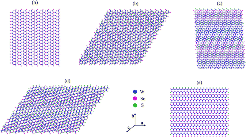 |
| | Fig. 1 Moiré patterns of the WS2/WSe2 heterostructure for twist angles of (a) 0°, (b) 16.10°, (c) 30°, (d) 47.48°, and (e) 60°. | |
To verify the dynamical stability of the twisted  heterostructure, we have calculated the phonon band structure along the high symmetric points (X–Γ–Y–Z) for
  heterostructures at θ = 0°, as shown in Fig. 2(a–d). From the phonon band structure, we can see that there is no negative frequency present. It means that the heterostructures are dynamically stable.
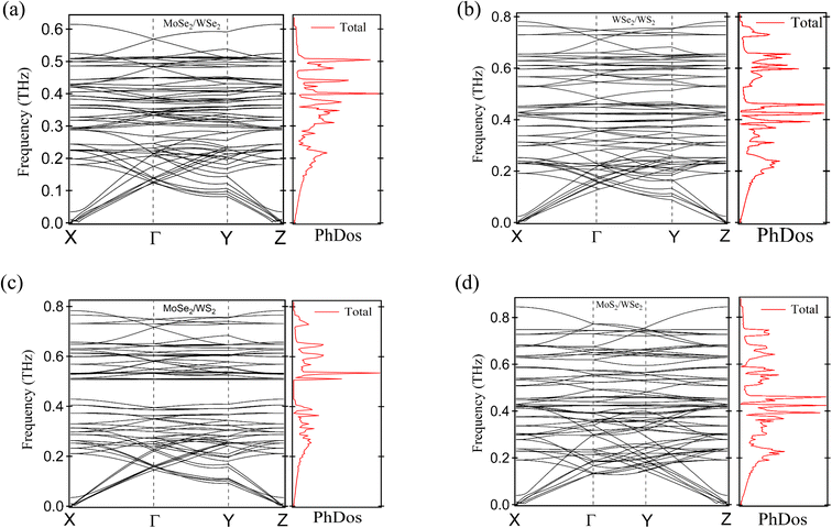 |
| | Fig. 2 The phonon dispersions of heterostructures at θ = 0°: (a) MoSe2/WSe2, (b) WSe2/WS2, (c) MoSe2/WS2 and (d) MoS2/WSe2. | |
To check, whether the structure is thermodynamically stable or not, we calculate the binding energies (Eb) of the twisted  heterostructures using the following formula:
| |
 | (1) |
where

,
EMX2 and

represent the respective total energies of

, MX
2 and

. Here, M and M′ are transition metals, X and X′ are chalcogens and
N is the number of atoms in the supercell. The calculated binding energies of the heterostructures MoSe
2/WSe
2, WS
2/WSe
2, MoSe
2/WS
2 and MoS
2/WSe
2 vary from 18.24 to 30.37 meV, 13.55 to 42.55 meV, 17.93 to 64.66 meV, and 13.07 to 69.43 meV respectively with the twisting angle, as shown in Fig. S3 in the ESI.
†52 The low binding energies for the heterostructures lead to feasible structures.
3.2. Electronic properties
To explore the electronic properties of the twisted heterostructure, the fat band structures have been calculated along the path X–Γ–Y–Z with the corresponding projected density of states (PDOS). Fig. 3 and S4†52 show the fat band structures and projected density of states of twisted WS2/WSe2 and MoSe2/WSe2 heterostructures. The overlapping of spin ↑ and spin ↓ bands in the calculated band structure demonstrates the non-magnetic behavior of the twisted TMD heterostructures. Furthermore, the heterostructure exhibits a semiconducting behavior across various twist angles. Fig. 4 illustrates the variation of bandgap as a function of twist angle for these heterostructures. The band gap varies between 1.02 to 1.42 eV, 0.67 to 1.03 eV, 1.02 to 1.30 eV, and 0.76 to 1.24 eV for MoSe2/WSe2, MoSe2/WS2, WS2/WSe2, and MoS2/WSe2 heterostructures respectively, which switches between direct and indirect band gaps as a function of twist angle (θ) for all the twisted heterostructures except WS2/WSe2, for which all the band gaps are found to be indirect. MoSe2/WSe2 (θ = 0°, 60°), MoSe2/WS2 (θ = 0°, 60°), MoS2/WSe2 (θ = 0° 16.10°, 21.79°, 43.9°, 60°) have a direct bandgap, which is crucial for improving the performance of photonic devices. We can see that both the valence band maximum (VBM) and conduction band minimum (CBM) are located at the Γ point for all the twisted heterostructures (see Fig. S4†).52 The direct band gaps are more desirable for optical applications due to the easy optical transition of electrons from the valence band to the conduction band.
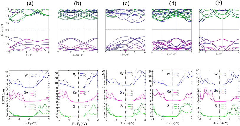 |
| | Fig. 3 The fat band structure and projected density of states of the twisted WSe2/WS2 heterostructure for twist angles of (a) 0°, (b) 16.10°, (c) 30°, (d) 47.48°, and (e) 60°. Blue, pink, and green bands represent contributions from W, Se and S atoms respectively. | |
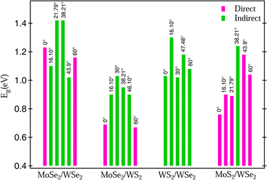 |
| | Fig. 4 Variation of bandgap of MoSe2/WSe2, MoSe2/WS2, WS2/WSe2 and MoS2/WSe2 heterostructures for different twist angles. | |
To get more insight into the individual contribution of atomic orbitals in the bands, we study the projected density of states (PDOS). From PDOS analysis of the WS2/WSe2 heterostructure (see Fig. 3), we observe that for θ = 0°, the px orbital of the Se atom and the eg orbital of the W atom are the main contributors to the valence band (VB), with small contributions from the py orbitals of the S atom, whereas the conduction band (CB) originates from the eg orbitals of the W atom and pz orbital of the S atom with less contribution from the px orbital of the Se atom. In contrast, a reversed nature of the PDOS was observed for θ = 16.10°, the eg orbital of the W atom and py orbitals of the Se atom are higher contributing for the valence band maximum (VBM) whereas for the conduction band (CB) the p orbital of the S atom and eg orbitals of the W atom contribute more with less contribution from the p orbital of the Se atom, and so on. These contributions are influenced by the change in crystal structure through the application of twist. When a twist is applied to a crystal structure, it causes a change in the arrangement of atoms, resulting in the change in hybridization of different orbitals. This orbital hybridization leads to a shift in the positions of the conduction band minimum (CBM) and valence band maximum (VBM), which in turn allows for the modulation of bandgaps and offers opportunities for tailoring the electronic properties of materials.53
Fig. 5 shows the variation of the effective mass of holes and electrons with different twist angles along the Γ → X and Γ → Y directions for  heterostructures. Using the curvature of the energy band at the conduction band minimum (CBM) and valence band maximum (VBM), we can calculate the electron and hole effective masses:
| |
 | (2) |
where
E is total energy, ℏ is reduced Planck’s constant, and
k is the wave vector. We have calculated the effective mass of holes and electrons (in units of
m0, free electron mass) at the points of VBM and CBM in the path of Brillouin zone
Γ →
X and
Γ →
Y directions with varying twist angle (
θ). For MoSe
2/WSe
2, the effective mass of holes

along the
y-direction starts to increase from 0.437
m0 and remains nearly constant at around 2.179
m0, then suddenly decreases to 1.351
m0 at 60° while the effective mass of electrons

along the
y-direction initially decreases from 1.039
m0 to 0.685
m0 as the angle changes from 0° to 16.10°, then it shows a sudden decrease and remains steady at 21.79° and 38.21°. After that, it again increases to 0.635
m0 at 43.9°. In the case of WS
2/WSe
2, MoSe
2/WS
2 and MoS
2/WSe
2, the effective mass of holes varies between 0.436
m0 to 1.442
m0, 0.624
m0 to 2.062
m0 and 0.414
m0 to 1.738
m0 along the
y-direction, with twist angle, respectively. Whereas, the effective mass of electrons varies around 0.320
m0 to 2.212
m0, 0.338
m0 to 2.673
m0 and 0.007
m0 to 0.470
m0 for WS
2/WSe
2, MoSe
2/WS
2 and MoS
2/WSe
2, respectively. The estimated value of effective mass doesn’t change as much as in going along the
x- and
y-directions except at a few twist angles. It is noted that the MoS
2/WSe
2 heterostructure has a low effective mass for twist angles 16.10°, 21.79°, and 43.9° compared to MoSe
2/WSe
2, WS
2/WSe
2, MoSe
2/WS
2 heterostructures, making the MoS
2/WSe
2 heterostructure suitable for high-performance electronic device applications since a lighter electron effective mass can enhance mobility. The obvious change in effective mass with twist suggests that twist angle can modulate carrier mobilities in 2D heterostructures.
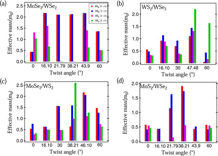 |
| | Fig. 5 Variation of effective mass of (a) MoSe2/WSe2, (b) WS2/WSe2, (c) MoSe2/WS2 and (d) MoS2/WSe2 heterostructures for different twist angles. | |
3.3. Optical properties
To further interpret the possible applications of TMD heterostructures in optoelectronic devices, we employ the frequency-dependent dielectric function, ε(ω) = ε1(ω) + iε2(ω), to calculate the optical properties of the  heterostructure. The real part, ε1(ω), and the imaginary part, ε2(ω), of the dielectric constant are evaluated using the Kubo–Greenwood formalism.47 This formalism can be expressed as follows:
| |
 | (3) |
where the dipole transition matrix element pnmi = 〈nk|pi|mk〉 is the ith component of the momentum operator between states n and m, M represents the mass of electron, volume (V), and Γ represents energy broadening. fnk is the Fermi function evaluated at the band energy En(k) and ℏωnm = En − Em. The complex dielectric constant relates to the susceptibility tensor as:
The imaginary component of the complex dielectric function, ε2(ω), is obtained from the momentum matrix elements between the occupied and unoccupied electronic states. Mathematically, this could be expressed as:
| |
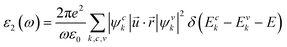 | (5) |
where
ψck and
ψvk are the conduction band and valence band wave functions
k points,
ω is the angular frequency of electromagnetic radiation in energy units,
ε0 is the free space permittivity.

and

denote the polarization vector and position vector of the EM field respectively.
On the other hand, the real part of the dielectric function, ε1(ω), is determined from the ε2(ω) by using the Kramers–Kronig transformation.46
| |
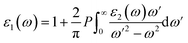 | (6) |
where
P is the principal value of the integral.
The optical studies have been performed considering the propagation of light perpendicular to the z-direction. Here, we observe equivalent contributions of optical properties of the heterostructure in the x- and y-directions. Fig. 6(a and b) and S6(a and b)† show the variation of the real and imaginary parts of the dielectric constant ε(ω) of the WS2/WSe2 and MoSe2/WS2 heterostructures respectively under various twist angles. It can be seen that the real and imaginary parts of the dielectric function are modulated by varying the twist angle. Due to hexagonal crystal symmetry, the  heterostructure exhibits isotropic behavior in the x and y directions. The key feature of the ε1(ω) plot is the ω = 0 on the y-axis, also referred to as the static value. The square root of the static value gives the refractive index values. The static dielectric constants vary from 1.23 to 1.29, and 1.16 to 1.23 for WS2/WSe2, and MoSe2/WS2 heterostructures, respectively. The maximum values of the ε1(ω = 0) for WS2/WSe2, and MoSe2/WS2 are observed to be 1.29 for θ = 16.10°, and 1.23 for θ = 46.10° respectively. For WS2/WSe2, the real part of the dielectric constant starts to increase with photon energy and it peaks at 1.45 eV, 1.6 eV, 1.55 eV, 1.6 eV, and 1.5 eV, after that, it starts to decrease to a minimum value at 2.2 eV, 2.35 eV, 2.55 eV, 2.4 and 2.45 eV and then further increase for 0°, 16.10°, 30°, 47.48°, and 60° twist angle respectively. The peaks in the imaginary part of the dielectric function ε2(ω) are caused by transitions of electrons between the valence band to the conduction band. The peak position indicates the energy level at which electronic transition occurs, which is influenced by the band structure and electronic properties of the material. For the WS2/WSe2 heterostructure, the first peak is located at 1.55 eV (θ = 0°), 1.85 eV (θ = 16.10°), 1.8 eV (θ = 30°), 1.85 (θ = 47.48°) and 1.6 (θ = 60°) similar to the band gaps of 1.03 eV, 1.30 eV, 1.02 eV, 1.18 eV, and 1.08 eV, which correspond to the transition from px (Se) to pz (S), eg (W) to p (S), eg (W) to px (S), eg (W) to px (S), and px (Se) to pz (S), respectively. In the case of MoSe2/WS2, the first peak is located at 1.5 eV (θ = 0°), 1.55 eV (θ = 16.10°), 1.55 eV (θ = 30°), 1.6 eV (θ = 38.21°) and 1.6 eV (θ = 46.10°) similar to the band gaps of 0.76 eV, 1.43 eV, 0.89 eV, 1.24 eV, and 1.18 eV, respectively.
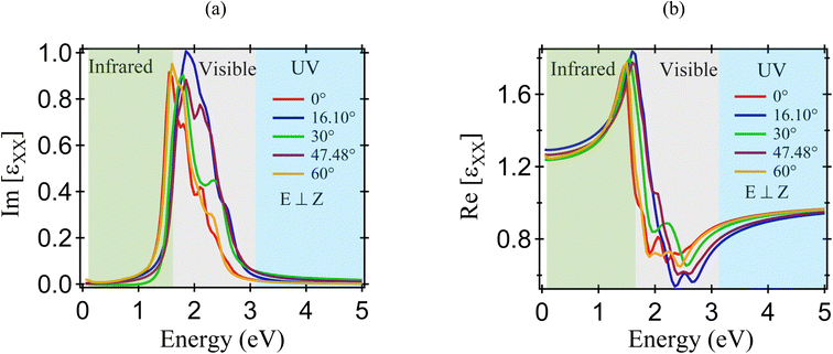 |
| | Fig. 6 (a) Variation of the imaginary part of the dielectric constant ε2(ω) and (b) the real part of the dielectric constant ε1(ω) plotted as a function of photon energy (0–5 eV) along the x-direction for the WS2/WSe2 heterostructure for different twist angles. | |
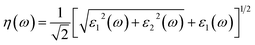
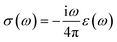
The optical properties such as absorption coefficient (α(ω)), refractive index (η), extinction coefficient (κ), and optical conductivity σ(ω) can be determined from ε1(ω) and ε2(ω).
3.3.1. Absorption coefficient. The absorption coefficient α(ω) can be determined from equation:| |
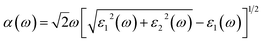 | (7) |
Fig. 7(a) and S7(a)† show the absorption coefficients for WS2/WSe2 and MoSe2/WS2 heterostructures. An absorption coefficient is a measure of how much light a medium absorbs. There are many peaks within the energy range of 0–5 eV. The overall change trend is similar, and the only difference is in the peak values. The absorption coefficient shows the highest peak for WS2/WSe2 at 1.85 eV, 2.05 eV, 1.85 eV, 2.3 eV, and 1.8 eV for twist angles of 0°, 16.10°, 30°, 47.48°, and 60°, respectively, after that it falls sharply. In the case of the MoSe2/WS2 heterostructure, the highest absorption peak occurs at 1.5 eV, 1.75 eV, 1.6 eV, 1.65 eV, and 1.7 eV for twist angles 0°, 16.10°, 30°, 38.21°, and 46.10°, respectively. These absorption peaks correspond to the transition of electrons from valence bands to conduction bands in the material and show maximum light absorption for these wavelengths. Due to material properties, it can be used for wavelength filtering purposes in that region.54 The optical band gap of a material is determined by the threshold value of photon energy at which the absorption spectra starts to increase or when an optical transition occurs. The optical band gap for the WS2/WSe2 heterostructure is found to be 0.9 eV for 0°, 0.9 eV for 16.10°, 0.95 eV for 30°, 0.85 eV for 47.48° and 0.75 eV for 60°. In the case of the MoSe2/WS2 heterostructure, the optical gap is 0.7 eV for 0°, 1.1 eV for 16.10°, 0.45 eV for 30°, 0.95 eV for 38.21° and 0.95 eV for 46.10°. It is important to note that the electronic band gap is consistently larger than the optical band gap due to excitonic binding energy. For photon energies below the optical gap, the material appears transparent. The absorption area lies between 1.3 eV to 2.85 eV, and 1.2 eV to 2.25 eV for WS2/WSe2 and MoSe2/WS2 heterostructures, respectively. Hence, this area is highly sensitive to optical absorption. As we can see here these heterostructures show excellent optical absorption in the visible light region (1.7 to 3.1 eV), less absorption in the infrared region, and become transparent in the UV region (energy greater than 3.2 eV). This shows that the proposed heterostructures can be utilized for photovoltaic applications.
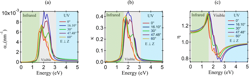 |
| | Fig. 7 (a) Absorption coefficient α(ω), (b) extinction coefficient (κ), and (c) refractive index (η) plotted as a function of photon energy (0–5 eV) along the x-direction for the WS2/WSe2 heterostructure at different twist angles. | |
3.3.2. Refractive index and extinction coefficient. The complex refractive index can be defined as ñ(ω) = n(ω) + iκ(ω), where η(ω) and κ(ω) are the real and imaginary parts (extinction coefficient) of the complex refractive index and can be determined from ε1(ω) and ε2(ω) using the following equations:| |
 | (8) |
| |
 | (9) |
Here, ω is the angular frequency.The variations of refractive index with photon energy at different twist angles for WS2/WSe2 and MoSe2/WS2 are shown in Fig. 7(c) and S7(c).† From eqn (8), it is clear that the refractive index depends on the real and imaginary parts of the dielectric constant. By comparing the plot of the real part of the dielectric constant Fig. 6(b) and the refractive index Fig. 7(c), the change in trends in Fig. 6(b) and 7(c) are comparable, indicating that the refractive index is mostly affected by the real part of the dielectric constant. The values of the static refractive index for WS2/WSe2 (see Fig. 7(c)) and MoSe2/WS2 (see Fig. S7(a)†) heterostructure vary in the range from 1.11 to 1.14 and 1.08 to 1.11, respectively, as we twist the heterostructure from 0° to 60°. For WS2/WSe2 the highest value of the refractive index is observed to be 1.33 at 1.45 eV, 1.39 at 1.65 eV, 1.35 at 1.55 eV, 1.34 at 1.65 eV and 1.35 at 1.5 eV with the twisting angles of 0°, 16.10°, 30°, 47.48° and 60°, respectively. Thereafter, the refractive indices decrease steadily and further increases, then tend to be constant in the UV region. In the case of MoSe2/WS2, the highest value of the refractive index is observed to be 1.25 at 1.35 eV, 1.3 at 1.4 eV, 1.28 at 1.4 eV, 1.35 at 1.4 eV and 1.33 at 1.45 eV with twist angles 0°, 16.10°, 30°, 38.21° and 46.10°, respectively (Table 2). The rotation angles provide further flexibility for using the same material in different applications with low and high values of refractive index. High refractive index materials find application in energy storage devices such as solar cells; they are used as a coating to enhance light trapping and absorption within the solar cell, whereas a material with low refractive index shows great potential for photonic device applications due to high reflectivity.55
Table 2 Variation of refractive index with twist angle for different TMD heterostructures
| θ (°) |
Refractive index |
| MoSe2/WSe2 |
WS2/WSe2 |
MoSe2/WS2 |
MoS2/WSe2 |
| 0 |
1.34 |
1.34 |
1.25 |
1.43 |
| 16.1 |
1.2 |
1.37 |
1.3 |
1.7 |
| 21.79 |
1.34 |
— |
— |
1.38 |
| 30 |
— |
1.35 |
1.28 |
— |
| 38.21 |
1.35 |
— |
1.35 |
1.37 |
| 43.9 |
1.2 |
— |
— |
1.28 |
| 46.1 |
— |
— |
1.33 |
— |
| 47.48 |
— |
1.34 |
— |
— |
| 60 |
1.34 |
1.35 |
— |
1.37 |
Fig. 7(b) and S7(b)† show the variation of extinction coefficient with photon energy at different twist angles for WS2/WSe2 and MoSe2/WS2. The extinction coefficients are correlated with absorption coefficients. An area with a high extinction coefficient has a high absorption capacity. The highest value of extinction coefficient for WS2/WSe2 is observed to be 0.38 at 1.6 eV, 0.44 at 2 eV, 0.39 at 1.8 eV, 0.37 at 1.85 eV, and 0.41 at 1.8 eV with the twisting angles of 0°, 16.10°, 30°, 47.48°, and 60°, respectively. For MoSe2/WS2, the highest value of extinction coefficient is observed to be 0.33 at 1.5 eV, 0.36 at 1.75 eV, 0.43 at 1.6 eV, 0.47 at 1.6 eV, and 0.41 at 1.7 eV with twist angles 0°, 16.10°, 30°, 38.21°, and 46.10°, respectively. The peak height drops in the visible region, which tends to be constant after 4 eV.
3.3.3. Optical conductivity. In general, optical conductivity is a complex quantity. By using the dielectric function, we can calculate the optical conductivity:| |
 | (10) |
The real and imaginary parts of optical conductivity are given by
| |
 | (11) |
| |
 | (12) |
In complex optical conductivity, the real component is called photoconductivity (optical conductivity). Optical conductivity is a measure of free carriers generated in a material when exposed to light of a suitable wavelength. A material with more free carriers under irradiation will have a greater optical conductivity. It varies from 194.3 to 258.3 A V−1 cm−1, and 145.2 to 228.7 A V−1 cm−1 for WS2/WSe2 and MoSe2/WS2 heterostructures, respectively, with the twisting angle. The maximum values of optical conductivity for WS2/WSe2 and MoSe2/WS2 heterostructures are found to be 258.3 A V−1 cm−1 at 1.9 eV for 16.10°, and 228.7 A V−1 cm−1 at 1.6 eV for 38.21°. Among all of the twisting angles, MoSe2/WSe2, WS2/WSe2, MoSe2/WS2, and MoS2/WSe2 heterostructures show the highest optical absorption at 60°, 16.10°, 38.21°, and 16.10°, respectively, which is the most favorable twisting angle for optical response in the heterostructure. The outstanding optical properties of  heterostructures make them highly suitable for applications in photovoltaic and optical devices.
4. Conclusion
Here, we have performed a systematic and comparative study on electronic and optical properties of MoSe2/WSe2, MoS2/WSe2, WS2/WSe2 and MoSe2/WS2 heterostructures with different twist angles, by using density functional theory (DFT) based first-principles calculations. Firstly, our calculations show that twisted  heterostructures exhibit dynamical and thermodynamic stability. Then, we have shown the variation of the band gap, in which an indirect to direct band gap transition appears, i.e., the electronic properties of the
  heterostructures can be effectively tuned by interlayer coupling. In addition, MoSe2/WSe2 (θ = 0°, 60°), MoSe2/WS2 (θ = 0°, 60°), MoS2/WSe2 (θ = 0°, 16.10°, 21.79°, 43.9°, and 60°) have a direct band gap, and therefore they are suitable for photovoltaic applications. Also, optical properties such as the refractive index, the extinction coefficient, and the absorption coefficient have been calculated for
  heterostructures with twist angle. The MoSe2/WSe2, WS2/WSe2, MoSe2/WS2, and MoS2/WSe2 heterostructures exhibit high sensitivity in the visible regions and demonstrate excellent optical absorption at specific twist angles: 60°, 16.10°, 38.21°, and 16.10° respectively. These findings provide valuable insights into the impact of twist on vertically stacked
  heterostructures, making them promising materials for various optoelectronic devices and light-emitting diodes (LEDs), including solar cell applications. This is due to their direct band gap semiconductor properties and high absorption coefficients.
Conflicts of interest
There are no conflicts to declare.
Acknowledgements
NG acknowledges the DST INSPIRE (No. IF200524) for financial assistance. The authors gratefully acknowledge the support and resources provided by the ‘PARAM Kamrupa’ Facility at the IIT Guwahati under the National Supercomputing Mission of Government of India.
References
- K. S. Novoselov, A. K. Geim, S. V. Morozov, D. Jiang, Y. Zhang, S. V. Dubonos, I. V. Grigorieva and A. A. Firsov, Electric field effect in atomically thin carbon films, Science, 2004, 306(5696), 666–669 CrossRef CAS PubMed.
- A. Chaudhury, S. Majumder and S. J. Ray, Proximity-induced colossal conductivity modulation in phosphorene, Phys. Rev. Appl., 2019, 11(2), 024056 CrossRef CAS.
- S. Rani and S. J. Ray, Two-dimensional C3N based sub-10 nanometer biosensor, Phys. Chem. Chem. Phys., 2020, 22(20), 11452–11459 RSC.
- R. Fei, W. Li, L. Ju and L. Yang, Giant piezoelectricity of monolayer group IV monochalcogenides: SnSe, SnS, GeSe, and GeS, Appl. Phys. Lett., 2015, 107(17), 173104 CrossRef.
- S. J. Ray, First-principles study of MoS2, phosphorene and graphene based single electron transistor for gas sensing applications, Sens. Actuators, B, 2016, 222, 492–498 CrossRef CAS.
- X. Zhou, N. Zhou, C. Li, H. Song, Q. Zhang, X. Hu and L. Gan, et al., Vertical heterostructures based on SnSe2/MoS2 for high performance photodetectors, 2D Mater., 2017, 4(2), 025048 CrossRef.
- T. Heine, Transition metal chalcogenides: ultrathin inorganic materials with tunable electronic properties, Acc. Chem. Res., 2015, 48(1), 65–72 CrossRef CAS PubMed.
- H. Wang, H. Yuan, S. S. Hong, Y. Li and Y. Cui, Physical and chemical tuning of two-dimensional transition metal dichalcogenides, Chem. Soc. Rev., 2015, 44(9), 2664–2680 RSC.
- B. Peng, L. Qi, X. Liang, P. Song, J. Li, K. He and D. Fu, et al., Valley polarization of trions and magnetoresistance in heterostructures of MoS2 and yttrium iron garnet, ACS Nano, 2017, 11(12), 12257–12265 CrossRef CAS PubMed.
- W. Bao, L. Jing, J. Velasco Jr, Y. Lee, G. Liu, D. Tran and B. Standley, et al., Stacking-dependent band gap and quantum transport in trilayer graphene, Nat. Phys., 2011, 7(12), 948–952 Search PubMed.
- Z. Liu, M. Amani, S. Najmaei, Q. Xu, X. Zou, Z. Wu and Y. Ting, et al., Strain and structure heterogeneity in MoS2 atomic layers grown by chemical vapour deposition, Nat. Commun., 2014, 5(1), 1–9 Search PubMed.
- Z. Zhao, H. Zhang, H. Yuan, S. Wang, Y. Lin, Q. Zeng and G. Xu, et al., Pressure induced metallization with absence of structural transition in layered molybdenum diselenide, Nat. Commun., 2015, 6(1), 7312 Search PubMed.
- J. He, K. Hummer and C. Franchini, Stacking effects on the electronic and optical properties of bilayer transition metal dichalcogenides MoS2, MoSe2, WS2, and WSe2, Phys. Rev. B: Condens. Matter Mater. Phys., 2014, 89(7), 075409 CrossRef.
- M. N. Ali, J. Xiong, S. Flynn, T. Jing, Q. D. Gibson, L. M. Schoop and L. Tian, et al., Large, non-saturating magnetoresistance in WTe2, Nature, 2014, 514(7521), 205–208 CrossRef CAS PubMed.
- A. K. Geim and I. V. Grigorieva, Van der Waals heterostructures, Nature, 2013, 499(7459), 419–425 CrossRef CAS PubMed.
- Z. Zheng, M. Cox and B. Li, Surface modification of hexagonal boron nitride nanomaterials: a review, J. Mater. Sci., 2018, 53, 66–99 CrossRef CAS.
- P. Lambin, H. Amara, F. Ducastelle and L. Henrard, Long-range interactions between substitutional nitrogen dopants in graphene: electronic properties calculations, Phys. Rev. B: Condens. Matter Mater. Phys., 2012, 86(4), 045448 CrossRef.
- X. Dai, F. Zhu, Z. Qian and J. Yang, Electric potential and carrier distribution in a piezoelectric semiconductor nanowire in time-harmonic bending vibration, Nano Energy, 2018, 43, 22–28 CrossRef CAS.
- S. J. Ray and M. Venkata Kamalakar, Unconventional strain-dependent conductance oscillations in pristine phosphorene, Phys. Chem. Chem. Phys., 2018, 20(19), 13508–13516 RSC.
- S. Sachin, P. Kumari, N. Gupta, S. Rani, S. Kar and S. J. Ray, Van der Waals twistronics in a MoS2/WS2 heterostructure, Comput. Condens. Matter, 2023, 35, e00797 CrossRef.
- S. Sachin, S. Rani, P. Kumari, S. Kar and S. J. Ray, Twist-engineered tunability in vertical MoS2/MoSe2 heterostructure, Appl. Phys. A, 2023, 129(1), 46 CrossRef CAS.
- S. Kar, P. Kumari, M. Venkata Kamalakar and S. J. Ray, Twist-assisted optoelectronic phase control in two-dimensional (2D) Janus heterostructures, Sci. Rep., 2023, 13(1), 13696 CrossRef CAS PubMed.
- S. Rani and S. J. Ray, DNA and RNA detection using graphene and hexagonal boron nitride based nanosensor, Carbon, 2021, 173, 493–500 CrossRef CAS.
- S. Sahoo, P. Kumari and S. J. Ray, Promising cathode material MnO2/CoO2 heterostructure for the Li and Na ion battery: A computational study, J. Appl. Phys., 2023, 134, 104302 CrossRef CAS.
- Y. Cao, F. Valla, S. Fang, K. Watanabe, T. Taniguchi, E. Kaxiras and P. Jarillo-Herrero, Unconventional superconductivity in magic-angle graphene superlattices, Nature, 2018, 556(7699), 43–50 CrossRef CAS PubMed.
- S. J. Ahn, P. Moon, T.-H. Kim, H.-W. Kim, H.-C. Shin, E. H. Kim and H. W. Cha, et al., Dirac electrons in a dodecagonal graphene quasicrystal, Science, 2018, 361(6404), 782–786 CrossRef CAS PubMed.
- N. Gupta, S. Rani, P. Kumari, R. Ahuja and S. J. Ray, Ultralow lattice thermal conductivity and thermoelectric performance of twisted Graphene/Boron Nitride heterostructure through strain engineering, Carbon, 2023, 215, 118437 CrossRef CAS.
- K. Tran, G. Moody, F. Wu, X. Lu, J. Choi, K. Kim and A. Rai, et al., Evidence for Moiré excitons in van der Waals heterostructures, Nature, 2019, 567(7746), 71–75 CrossRef CAS PubMed.
- J. Shi, Y. Li, Z. Zhang, W. Feng, Q. Wang, S. Ren, J. Zhang, W. Du, X. Wu, X. Sui, Y. Mi, R. Wang, Y. Sun, L. Zhang, X. Qiu, J. Lu, C. Shen, Y. Zhang, Q. Zhang and X. Liu, Twisted-angle-dependent optical behaviors of intralayer excitons and trions in WS2/WSe2 heterostructure, ACS Photonics, 2019, 6, 3082–3091 CrossRef CAS.
- L. Wang, E.-M. Shih, A. Ghiotto, L. Xian, D. A. Rhodes, C. Tan and C. Martin, et al., Correlated electronic phases in twisted bilayer transition metal dichalcogenides, Nat. Mater., 2020, 19(8), 861–866 CrossRef CAS PubMed.
- X.-G. Gao, X.-K. Li, W. Xin, X.-D. Chen, Z.-B. Liu and J.-G. Tian, Fabrication, optical properties, and applications of twisted two-dimensional materials, Nanophotonics, 2020, 9(7), 1717–1742 CrossRef CAS.
- B. Tang, B. Che, M. Xu, Z. P. Ang, J. Di, H.-J. Gao, H. Yang, J. Zhou and L. Zheng, Recent advances in synthesis and study of 2D twisted transition metal dichalcogenide bilayers, Small Struct., 2021, 2(5), 2000153 CrossRef CAS.
- R. Ribeiro-Palau, C. Zhang, K. Watanabe, T. Taniguchi, J. Hone and C. R. Dean, Twistable electronics with dynamically rotatable heterostructures, Science, 2018, 361(6403), 690–693 CrossRef CAS.
- K. Kim, M. Yankowitz, B. Fallahazad, S. Kang, H. C. P. Movva, S. Huang and S. Larentis, et al., van der Waals heterostructures with high accuracy rotational alignment, Nano Lett., 2016, 16(3), 1989–1995 CrossRef CAS PubMed.
- K. Chen, X. Wan, J. Wen, W. Xie, Z. Kang, X. Zeng, H. Chen and J.-B. Xu, Electronic properties of MoS2–WS2 heterostructures synthesized with two-step lateral epitaxial strategy, ACS Nano, 2015, 9(10), 9868–9876 CrossRef CAS PubMed.
- Y. Gong, S. Lei, G. Ye, B. Li, Y. He, K. Keyshar and X. Zhang, et al., Two-step growth of two-dimensional WSe2/MoSe2 heterostructures, Nano Lett., 2015, 15(9), 6135–6141 CrossRef CAS PubMed.
- X. Chen, Y. Qiu, H. Yang, G. Liu, W. Zheng, W. Feng, W. Cao, W. Hu and P. A. Hu, In-plane mosaic potential growth of large-area 2D layered semiconductors MoS2–MoSe2 lateral heterostructures and photodetector application, ACS Appl. Mater. Interfaces, 2017, 9(2), 1684–1691 CrossRef CAS PubMed.
- S. Smidstrup, T. Markussen, P. Vancraeyveld, J. Wellendorff, J. Schneider, T. Gunst and B. Verstichel, et al., QuantumATK: an integrated platform of electronic and atomic-scale modelling tools, J. Phys.: Condens. Matter, 2020, 32(1), 015901 CrossRef CAS PubMed.
- J. Zhang, L. Ma, M. Zhang and J. Zhang, First principles study on the stability and thermodynamic properties of NAu co-doped graphene, Diamond Relat. Mater., 2020, 103, 107704 CrossRef CAS.
- J. E. Peralta, J. Heyd, G. E. Scuseria and R. L. Martin, Spin-orbit splittings and energy band gaps calculated with the Heyd-Scuseria-Ernzerhof screened hybrid functional, Phys. Rev. B: Condens. Matter Mater. Phys., 2006, 74(7), 073101 CrossRef.
- C.-H. Chang, X. Fan, S.-H. Lin and J.-L. Kuo, Orbital analysis of electronic structure and phonon dispersion in MoS2, MoSe2, WS2, and WSe2 monolayers under strain, Phys. Rev. B: Condens. Matter Mater. Phys., 2013, 88(19), 195420 CrossRef.
- K. F. Mak, C. Lee, J. Hone, J. Shan and T. F. Heinz, Atomically thin MoS2: a new direct-gap semiconductor, Phys. Rev. Lett., 2010, 105(13), 136805 CrossRef PubMed.
- H. R. Gutiérrez, N. Perea-López, A. L. Elías, A. Berkdemir, B. Wang, R. Lv, F. López-Urías, V. H. Crespi, H. Terrones and M. Terrones, Extraordinary room-temperature photoluminescence in triangular WS2 monolayers, Nano Lett., 2013, 13(8), 3447–3454 CrossRef PubMed.
- P. Tonndorf, R. Schmidt, P. Böttger, X. Zhang, J. Börner, L. Andreas and M. Albrecht, et al., Photoluminescence emission and Raman response of monolayer MoS2, MoSe2, and WSe2, Opt. Express, 2013, 21(4), 4908–4916 CrossRef CAS PubMed.
- S. Grimme, S. Ehrlich and L. Goerigk, Effect of the damping function in dispersion corrected density functional theory, J. Comput. Chem., 2011, 32(7), 1456–1465 CrossRef CAS PubMed.
- F. Wooten, Optical Properties of Solids, Academic Press, New York and London, 1972, vol. 9, pp. 803–804 Search PubMed.
- W. A. Harrison, Solid State Theory, McGraw-Hill, New York, London, Toronto, 1970 Search PubMed.
- C. L. Dong and J. Nocedal, On the limited memory BFGS method for large scale optimization, Math. Program., 1989, 45, 503–528 CrossRef.
- H. J. Monkhorst and J. D. Pack, Special points for Brillouin-zone integrations, Phys. Rev. B: Solid State, 1976, 13(12), 5188 CrossRef.
- A. Togo and I. Tanaka, First principles phonon calculations in materials science, Scr. Mater., 2015, 108, 1–5 CrossRef CAS.
- C. H. Chang, X. Fan, S. H. Lin and J. L. Kuo, Orbital analysis of electronic structure and phonon dispersion in MoS2, MoSe2, WS2 and WSe2 monolayers understrain, Phys. Rev. B: Condens. Matter Mater. Phys., 2013, 88, 195420 CrossRef.
- See the ESI†.
- S. Carr, D. Massatt, S. Fang, C. Paul, L. Mitchell and E. Kaxiras, Twistronics: Manipulating the electronic properties of two-dimensional layered structures through their twist angle, Phys. Rev. B, 2017, 95(7), 075420 CrossRef.
- H. Bennacer, S. Berrah, A. Boukortt and M. I. Ziane, Electronic and optical properties of GaInX2 (X= As, P) from first principles study, Indian J. Pure Appl. Phys., 2015, 53, 181–189 Search PubMed.
- E. F. Schubert, J. K. Kim and J.-Q. Xi, Low-refractive-index materials: A new class of optical thin-film materials, Phys. Status Solidi B, 2007, 244(8), 3002–3008 CrossRef CAS.
|
| This journal is © The Royal Society of Chemistry 2024 |
Click here to see how this site uses Cookies. View our privacy policy here. 
 Open Access Article
 This Open Access Article is licensed under a Creative Commons Attribution-Non Commercial 3.0 Unported Licence
 *
*
 (M = W, Mo; M′ = W; X = X′ = S, Se) heterostructures are less than 3.5% (see Table 1), which are quite small. The lowest lattice mismatch allows us to choose the twist angles of 0°, 16.10°, 21.79°, 30°, 43.9° and 60° for the
  heterostructures. The interlayer equilibrium distances (d) between MoSe2/WSe2, WS2/WSe2, MoSe2/WS2 and MoS2/WSe2 are 7.14 Å, 6.84 Å, 6.94 Å and 6.95 Å respectively, obtained from the energy curves as shown in Fig. S2 in the ESI,†52 where the energy is plotted as a function of interlayer distance for θ = 0°. The estimated interlayer distances between MoSe2/WSe2, WS2/WSe2, MoSe2/WS2 and MoS2/WSe2 vary in the range of 6.35 Å to 6.85 Å with twist angle ranging from 0° to 60°. The total number of atoms, strain, interlayer separation, and binding energy of TMD heterostructures with various twist angles are listed in Table 1. The top views of twisted WS2/WSe2 and MoSe2/WSe2 heterostructures for different twist angles are shown in Fig. 1 and S1†52 respectively.

 heterostructure, we have calculated the phonon band structure along the high symmetric points (X–Γ–Y–Z) for
  heterostructures at θ = 0°, as shown in Fig. 2(a–d). From the phonon band structure, we can see that there is no negative frequency present. It means that the heterostructures are dynamically stable.
 heterostructures using the following formula:
 , EMX2 and
  represent the respective total energies of
  , MX2 and
  . Here, M and M′ are transition metals, X and X′ are chalcogens and N is the number of atoms in the supercell. The calculated binding energies of the heterostructures MoSe2/WSe2, WS2/WSe2, MoSe2/WS2 and MoS2/WSe2 vary from 18.24 to 30.37 meV, 13.55 to 42.55 meV, 17.93 to 64.66 meV, and 13.07 to 69.43 meV respectively with the twisting angle, as shown in Fig. S3 in the ESI.†52 The low binding energies for the heterostructures lead to feasible structures.


 heterostructures. Using the curvature of the energy band at the conduction band minimum (CBM) and valence band maximum (VBM), we can calculate the electron and hole effective masses:
 along the y-direction starts to increase from 0.437 m0 and remains nearly constant at around 2.179 m0, then suddenly decreases to 1.351 m0 at 60° while the effective mass of electrons
  along the y-direction initially decreases from 1.039 m0 to 0.685 m0 as the angle changes from 0° to 16.10°, then it shows a sudden decrease and remains steady at 21.79° and 38.21°. After that, it again increases to 0.635 m0 at 43.9°. In the case of WS2/WSe2, MoSe2/WS2 and MoS2/WSe2, the effective mass of holes varies between 0.436 m0 to 1.442 m0, 0.624 m0 to 2.062 m0 and 0.414 m0 to 1.738 m0 along the y-direction, with twist angle, respectively. Whereas, the effective mass of electrons varies around 0.320 m0 to 2.212 m0, 0.338 m0 to 2.673 m0 and 0.007 m0 to 0.470 m0 for WS2/WSe2, MoSe2/WS2 and MoS2/WSe2, respectively. The estimated value of effective mass doesn’t change as much as in going along the x- and y-directions except at a few twist angles. It is noted that the MoS2/WSe2 heterostructure has a low effective mass for twist angles 16.10°, 21.79°, and 43.9° compared to MoSe2/WSe2, WS2/WSe2, MoSe2/WS2 heterostructures, making the MoS2/WSe2 heterostructure suitable for high-performance electronic device applications since a lighter electron effective mass can enhance mobility. The obvious change in effective mass with twist suggests that twist angle can modulate carrier mobilities in 2D heterostructures.

 heterostructure. The real part, ε1(ω), and the imaginary part, ε2(ω), of the dielectric constant are evaluated using the Kubo–Greenwood formalism.47 This formalism can be expressed as follows:

 and
and  denote the polarization vector and position vector of the EM field respectively.

 heterostructure exhibits isotropic behavior in the x and y directions. The key feature of the ε1(ω) plot is the ω = 0 on the y-axis, also referred to as the static value. The square root of the static value gives the refractive index values. The static dielectric constants vary from 1.23 to 1.29, and 1.16 to 1.23 for WS2/WSe2, and MoSe2/WS2 heterostructures, respectively. The maximum values of the ε1(ω = 0) for WS2/WSe2, and MoSe2/WS2 are observed to be 1.29 for θ = 16.10°, and 1.23 for θ = 46.10° respectively. For WS2/WSe2, the real part of the dielectric constant starts to increase with photon energy and it peaks at 1.45 eV, 1.6 eV, 1.55 eV, 1.6 eV, and 1.5 eV, after that, it starts to decrease to a minimum value at 2.2 eV, 2.35 eV, 2.55 eV, 2.4 and 2.45 eV and then further increase for 0°, 16.10°, 30°, 47.48°, and 60° twist angle respectively. The peaks in the imaginary part of the dielectric function ε2(ω) are caused by transitions of electrons between the valence band to the conduction band. The peak position indicates the energy level at which electronic transition occurs, which is influenced by the band structure and electronic properties of the material. For the WS2/WSe2 heterostructure, the first peak is located at 1.55 eV (θ = 0°), 1.85 eV (θ = 16.10°), 1.8 eV (θ = 30°), 1.85 (θ = 47.48°) and 1.6 (θ = 60°) similar to the band gaps of 1.03 eV, 1.30 eV, 1.02 eV, 1.18 eV, and 1.08 eV, which correspond to the transition from px (Se) to pz (S), eg (W) to p (S), eg (W) to px (S), eg (W) to px (S), and px (Se) to pz (S), respectively. In the case of MoSe2/WS2, the first peak is located at 1.5 eV (θ = 0°), 1.55 eV (θ = 16.10°), 1.55 eV (θ = 30°), 1.6 eV (θ = 38.21°) and 1.6 eV (θ = 46.10°) similar to the band gaps of 0.76 eV, 1.43 eV, 0.89 eV, 1.24 eV, and 1.18 eV, respectively.


 heterostructures make them highly suitable for applications in photovoltaic and optical devices.
 heterostructures exhibit dynamical and thermodynamic stability. Then, we have shown the variation of the band gap, in which an indirect to direct band gap transition appears, i.e., the electronic properties of the
  heterostructures can be effectively tuned by interlayer coupling. In addition, MoSe2/WSe2 (θ = 0°, 60°), MoSe2/WS2 (θ = 0°, 60°), MoS2/WSe2 (θ = 0°, 16.10°, 21.79°, 43.9°, and 60°) have a direct band gap, and therefore they are suitable for photovoltaic applications. Also, optical properties such as the refractive index, the extinction coefficient, and the absorption coefficient have been calculated for
  heterostructures with twist angle. The MoSe2/WSe2, WS2/WSe2, MoSe2/WS2, and MoS2/WSe2 heterostructures exhibit high sensitivity in the visible regions and demonstrate excellent optical absorption at specific twist angles: 60°, 16.10°, 38.21°, and 16.10° respectively. These findings provide valuable insights into the impact of twist on vertically stacked
  heterostructures, making them promising materials for various optoelectronic devices and light-emitting diodes (LEDs), including solar cell applications. This is due to their direct band gap semiconductor properties and high absorption coefficients.