
 Open Access Article
 This Open Access Article is licensed under a
 Creative Commons Attribution 3.0 Unported Licence
Interface-resolved photovoltage generation dynamics and band structure evolution in a PbS quantum dot solar cell†
Tamara
Sloboda
a,
Birgit
Kammlander
 ab,
Elin
Berggren
b,
Stefania
Riva
b,
Erika
Giangrisostomi
c,
Ruslan
Ovsyannikov
c,
Håkan
Rensmo
bd,
Andreas
Lindblad
b and
Ute B.
Cappel
*abd
ab,
Elin
Berggren
b,
Stefania
Riva
b,
Erika
Giangrisostomi
c,
Ruslan
Ovsyannikov
c,
Håkan
Rensmo
bd,
Andreas
Lindblad
b and
Ute B.
Cappel
*abd
aDivision of Applied Physical Chemistry, Department of Chemistry, KTH Royal Institute of Technology, SE-100 44 Stockholm, Sweden. E-mail: ute.cappel@physics.uu.se
bDivision of X-ray Photon Science, Department of Physics and Astronomy, Uppsala University, Box 516, SE-751 20, Uppsala, Sweden
cInstitute Methods and Instrumentation for Synchrotron Radiation Research, Helmholtz-Zentrum Berlin GmbH, Albert-Einstein-Straße 15, 12489 Berlin, Germany
dWallenberg Initiative Materials Science for Sustainability, Department of Physics and Astronomy, Uppsala University, 751 20 Uppsala, Sweden
First published on 22nd October 2024
Abstract
For directed development of solar cells using nanomaterials such as quantum dots, there is a need to understand the device function in detail. Understanding where photovoltage is generated in a device and where energy losses occur is a key aspect of this, and development of methods which can provide this information is needed. We have previously shown that time-resolved photoelectron spectroscopy of core levels can be used to follow the photovoltage dynamics at a specific interface of a lead sulfide quantum dot solar cell. Here, we use the method's selectivity and sample design to investigate the photovoltage generation in different parts of this solar cell and determine how the different layers (including the absorber layer thickness) contribute to charge separation. We show that all layers contribute to photovoltage generation and that a gold contact deposited on the quantum dots is necessary for full photovoltage generation and slow charge recombination. By combining the information obtained, we are able to experimentally follow the time evolution of the solar cell band structure during the charge separation process. Furthermore, we can identify which specific layers need to be optimized for an overall improvement of quantum dot cells. In the future, this methodology can be applied to other types of devices to provide insights into photovoltage generation mechanisms.
Introduction
Quantum dots (QDs) are of interest for a range of optoelectronic applications largely because their electronic properties can be tuned by their size. For solar cells, their bandgap and consequently their sunlight absorption characteristics can be tuned to be optimal in single or multijunction device structures.1–3 Furthermore, they can be fabricated by solution-based methods from abundant materials, which offers the possibility of cost-efficient manufacturing. Many of the most efficient quantum dot solar cells to date use lead sulfide as the main absorbing material in a layered device structure. In a typical device structure, an n-type PbS layer with a few hundred nanometer thickness is sandwiched between a conductive oxide substrate coated with an electron transport layer (ETL) and a hole transport layer (HTL) topped by an evaporated metal contact (typically gold).4–8 In the n-type layer, the PbS QDs are surrounded by halide ligands9–12 or a perovskite shell,5,13,14 and device efficiencies have been optimized through adjusting the ligand composition as well as ligand exchange methods.9,12,15,16 As charge transport in the quantum dots layers is expected to occur through a hopping mechanism,17–20 optimizing the ligands can lead to an improvement in charge carrier transport. The ETL is typically an n-type wide-bandgap metal oxide such as ZnO,4,21 or magnesium-doped ZnO (MZO).22,23 The HTL layer is often a thinner layer (about 50 nm) of PbS quantum dots, where the surface is terminated by with 1,2-ethanedithiol (EDT) ligands, which make the layer p-type.4,5,9,11,24Despite much recent progress through optimization of the device architecture, power conversion efficiencies of QD solar cells are still far below the theoretical limit. This has been attributed to recombination losses due to defects and poor charge transport, energy level mismatch of quantum dot layers and contacts and imbalanced charge extraction at contacts.5 Therefore, there is a need for more detailed investigations of device working mechanisms and, specifically, of the impact that each of the different layers has on the overall performance to aid achieving more efficient devices in the future. In particular, it is important to know how each layer contributes to the buildup of the photovoltage, how electric fields are distributed and where losses occur. These properties will be impacted by the timescales of charge transport, charge separation and recombination within the different layers of the device structure.
Charge recombination in PbS QD solar cells is often investigated through photovoltage decay measurements on complete devices. However, the timescales accessible in these measurements are often not short enough to investigate the kinetics of photovoltage generation and are also not selective to specific layers within a device structure. Time-resolved photoelectron spectroscopy (TRPES) with valence-to-conduction band excitations in the pump step can be used for detailed photovoltage kinetic characterization through measurements of core levels in the probe step. In photoelectron spectroscopy, only one external contact to the sample is needed for grounding to the spectrometer and if this contact is made through the sample substrate, the photovoltage between the sample surface and the substrate can be determined from core level shifts. The methodology is based on the premise that internal charge distributions and electrical fields induce the same shift to the frontier electronic structure as to the core levels. In this way, selected parts of the solar cell can be investigated by designing samples, which include or exclude specific layers from the device structure. Efficient measurements with picosecond time resolution can be achieved by combining a pulsed pump laser with a high repetition, pulsed X-ray source (such as provided by a synchrotron).
For bulk semiconductors, the photovoltage measured in TRPES is often associated with a surface photovoltage due to band bending towards the surface.25,26 However, we have shown that TRPES can also be used to determine the photovoltage generated between different layers in parts of a solar cell device.27 By using a pump laser with a relatively low repetition frequency (10 kHz) at a synchrotron beamline (PM4 at Bessy II28), we were able to study the photovoltage dynamics on timescales from pico- to microseconds in a single experiment. We demonstrated this method by investigating the dynamics of photovoltage generation and decay at the interface between PbS quantum dots with mixed PbI2/PbBr2 ligands (referred to as PbS-PbX2) and a MZO electron transport layer.27 In the study presented here, we used TRPES to investigate the photovoltage generation in different parts of a PbS quantum dot solar cell with a PbS-PbX2 absorber layer and an HTL consisting of PbS quantum dots with EDT ligands (PbS-EDT) by studying samples of different architectures (Fig. 1, top). This enabled us to compare photovoltage generation dynamics at different interfaces, identify loss mechanisms and suggest a charge generation mechanism for the complete solar cell.
 | ||
| Fig. 1 (Top) Architecture of samples and main elements of a TRPES experiment: X-ray and laser pulses impinging on, and electrons emitted from the sample surface. (Bottom) Band structure illustrations of the different samples based on literature data4,11 with the Fermi level (EF) in the dark indicated by the grey dashed line, the valence band edge (EV) indicated as the bottom of the field boxes and the conduction band edge (EC) as the top. | ||
Results and discussion
PbS quantum dots were synthesized as described in the methods section. The size of the synthesized quantum dots was determined from the exciton peak at 1.29 eV in the UV-visible absorption measurements to be about 3.15 nm (Fig. S1†).29 Solar cell type samples were prepared (see Experimental details). Fig. 1 shows the structures of these samples together with diagrams of band alignment and electrical field distributions in equilibrium as typically reported in literature for such solar cell architectures.4,11 We have previously demonstrated a power conversion efficiency of 10.7% and an open-circuit voltage of 0.66 V under 1 sun illumination.11 Three of the sample architectures (p-side, cell – no Au, and cell – Au) were prepared and measured for this study and compared to the results of the sample reported previously27 referred to as the n-side sample here. The sample surfaces were characterized through core level PES (Fig. S2†). We found the typical Pb 4f and S 2p signals of PbS quantum dots, as well as I 4d and Br 3d signals from the ligand shell. Some samples showed small additional sulphur features at binding energies higher than the main doublet, which indicate some oxidation of the surface. Where the top PbS layer has EDT ligands, somewhat higher surface oxidation was observed, in agreement with previous studies.11 For the “complete” cell, where the top layer consisted of a 5 nm thick gold layer, Pb 4f and S 2p peaks were still visible, but broadened and containing new contributions. This indicates that some chemical reactions occurred upon interface formation between PbS-EDT and Au.For the p-side samples and n-side samples of two different PbS-PbX2 thicknesses, we used core level positions to determine relative band edge positions in the dark based on a rigid band model, where core level shifts correspond to changes in the valence band position relative to the Fermi level. At a higher binding energy, the valence band edge is further away from the Fermi level (a more n-type state). From extended analysis of the data for the n-side samples presented in our previous study,27 the binding energy of the Pb 5d5/2 core level was at 19.4 eV for a 250 nm thick layer and at 19.5 eV for a 50 nm thick layer on an ITO/MZO substrate (Fig. S3†). This suggests that the thinner film has a slightly more n-type surface than the thicker film, in agreement with downward band bending towards the MZO substrate (Fig. 1). In the present study, we chose the Pb 4f core level for investigation (see Experimental details). For the p-side sample, the Pb 4f7/2 core level contribution assigned to PbS was found at a binding energy of 137.9 eV for the 250 nm thick sample and of 137.6 eV for the 50 nm thick sample (Fig. S3†). This agrees with upward band bending towards the EDT layer, as indicated in Fig. 1. In full cells, we therefore expect the band bending distribution across the junctions between the MZO/PbS-PX2 layers and between the PbS-PX2/PbS-EDT layers to follow the diagrams in Fig. 1. Overall, the core level positions at 250 nm thickness agree with an n-type character of the surface of a thick PbS-PbX2 layer on both substrates as observed in other studies.30–32
TRPES was carried by recording core level spectra with different delay times between a 515 nm pulsed pump laser and the X-ray probe (termed delay scans, see Experimental methods). Binding energy positions were determined through curve fitting and plotted as a function of delay times (termed kinetic traces, Fig. S4–S7†). Delay scans of the p-side samples showed core level shifts to higher binding energies upon laser illumination (Fig. S4–S6†) with a significantly larger magnitude for the 250 thick sample than for the 50 nm thick sample. For the n-side samples, it was previously observed that the Pb 5d core level shifts to higher binding energy upon laser illumination (Fig. S7†).27 This confirms that light-induced charge movement is in the opposite direction relative to the surface for the two sample designs: in the n-side samples electrons move into the n-type MZO substrate, while in the p-side sample holes move away from the surface and into the underlying layers. As the measurements at different delay times contain data at approximately the same long delay times (800 ns to 96 μs, see Experimental details), the sample stability during measurements could be confirmed by overlapping kinetic traces recorded in consecutive measurements (Fig. S4, S5 and S7†).27
To be able to gain information about absolute band edge shifts during illumination, we calculated averaged binding energies (B.E.) as a function of delay time (see details in Experimental methods) for the p-type (Fig. 2a) and n-type (Fig. 2b) samples (additional data at a lower laser pulse energy in Fig. S8†). Average binding energy positions in the dark are also included as horizontal solid lines for each delay scan. An offset is observed between the binding energy in the dark and the binding energies at long delay times for all delay scans, indicating that the systems do not return fully to the equilibrated dark state in the 96 μs timespan between two consecutive laser pulses. However, the measurement still captures important parts of the photovoltage generation and decay. From the energy difference between the binding energies under laser illumination and the binding energy in the dark, time-resolved photovoltages (V(t)) can be calculated according to:
 | (1) |
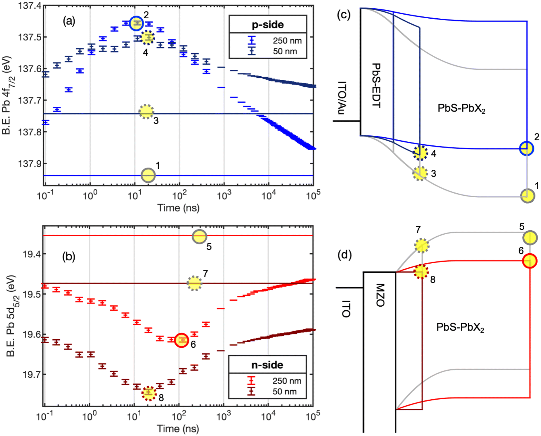 | ||
| Fig. 2 Kinetic traces of p-side and n-side samples and corresponding band diagrams. (a and b) Kinetic traces of averaged binding energies of p-side samples (ITO/Au/PbS-EDT/PbS-PbX2) (a) and n-side samples (ITO/MZO/PbS-PbX2) (b). Peak positions determined without laser included as horizontal lines. The laser intensity was 14.9 nJ per pulse for the p-side sample and 15.4 nJ per pulse for the n-side sample. (c and d) Schematic band diagrams of p-side (c) and n-side (d) samples at two different thicknesses in the dark (grey) and under illumination at maximum change in binding energy (blue, p-side; red, n-side) indicating the changes in valence band edge position for the p-side and the changes in conduction band position for the n-side. The yellow circles indicate the data points from which the band edge positions in the diagrams were drawn. Filled lines are used for the 250 nm samples and dashed lines for the 50 nm samples. | ||
The maximum values for the photovoltage, as well as the time at which this maximum occurs, are given in Table 1. The timescales of photovoltage generation showed a clear dependence on the PbS layer thickness for the n-side samples, as observed by the change in time at which the maximum photovoltage occurs (Table 1). For the p-side samples, changes in timescales were not observed; instead, the magnitude of the photovoltage depends strongly on the film thickness (Fig. 2). Furthermore, the generation of the photovoltage is faster for the thick PbS-PbX2 film on the p-type substrate than for the thick PbS-PbX2 film on the n-type substrate. This suggests that the charge transport and extraction of holes into the substrate is faster than that of electrons.
| Sample | d (nm) | Pulse energy (nJ) |
V
max,tot![[thin space (1/6-em)]](https://www.rsc.org/images/entities/char_2009.gif) b (V) b (V) |
t
maxc (ns) |
|---|---|---|---|---|
| a Thickness of PbS-PbX2 layer. b Maximum voltage determined from the binding energy difference to the equilibrated sample in dark. c Time at which maximum binding energy difference/maximum voltage is observed. d Values from ref. 27. | ||||
| N-side | 250 | 15.4 | −0.27 | 69d |
| N-side | 50 | 15.4 | −0.27 | 18d |
| P-side | 250 | 14.9 | 0.49 | 9.2 |
| P-side | 50 | 14.9 | 0.23 | 19 |
| Cell – no Au | 250 | 14.9 | −0.36 | 2.2 |
| Cell – Au | 250 | 14.9 | −0.67 | 10–100 |
Under the assumption that the substrate remains in equilibrium with the spectrometer, the maximum photovoltage corresponds to the maximum change in the band edge position. Other studies of PbS quantum dot films with halide ligands have shown core level shifts to higher binding energy under laser illumination.32,33 These shifts were significantly lower in magnitude (<50 meV) than the photovoltages observed here and were interpreted as a decrease in upwards band bending towards the surface upon illumination. Our study clearly shows that the substrate determines the sign of the photovoltage and that the absorber layer thickness influences the band edge positions. We therefore conclude that interfaces between different layers are the main cause of band bending and our energy diagrams are therefore drawn without additional surface band bending effects.
Band diagrams for the n-side and p-side samples in the dark and under illumination at the point of maximum charge separation drawn based on these conclusions are shown in Fig. 2. While these diagrams are partly schematic, the following can be highlighted: a thinner film in the p-side sample leads to the generation of a much smaller photovoltage, which has to be the result of less efficient charge separation and a smaller change in potential across the film. On the other hand, the n-side sample shows efficient charge separation also for a thin film as indicated by a similar maximum photovoltages for both film thicknesses. As the thinner film shows less overall band bending (as indicated by the higher binding energy position in the dark), charge separation in the thinner film will lead to a much flatter energy landscape (as shown in Fig. 2d). In the thicker film, charge separation may not complete due to slower charge separation dynamics, as discussed above.
Delay scans of the full cell sample configurations were also carried out. In absence of gold (cell – no Au), the Pb 4f core level was monitored (Fig. S9†). In presence of a 5 nm thick gold layer (cell – Au), delay scans were recorded for Au 4f and Pb 4f (Fig. S10 and S11†). The delay scans show the same binding energy shift for Pb 4f and Au 4f, but due to the better signal-to-noise ratio, the delay scan of Au 4f is shown in Fig. 3 below. Measurements of the cell – Au sample in the dark and comparison to a gold reference indicate that the photovoltage generated by the X-rays themselves in the sample is negligible (<0.03 eV, Fig. S12†). Measurements without laser can therefore be considered as indicative of the energy alignment in the dark at equilibrium.
 | ||
| Fig. 3 Kinetic traces of photovoltage determined from the difference in peak position with and without laser for the different samples with 250 nm thick PbS-PbX2 layers: p-side, n-side, cell – Au, and cell – no Au. The laser intensity was 14.9 nJ per pulse, except for the n-side sample, where it was 15.4 nJ per pulse. The schematic diagrams show the change in band alignment between the dark state (grey) and the state with maximum photovoltage for the 4 different samples (p-side, blue; n-side, red; Cell – Au, yellow; Cell – no Au, purple). | ||
Fig. 3 shows the photovoltage determined from the delay scans as a function of pump–probe delay time of the cell – Au and cell – no Au samples compared to the n-side and p-side samples with a common PbS-PbX2 thickness of 250 nm. The maximum photovoltage and the delay time at which the maximum photovoltage are observed (determined from multiexponential fitting to the kinetic traces) are given in Table 1. Both the cell – Au and the cell – no Au samples show binding energy shifts in the same direction as the n-side sample, in agreement with charge accumulation and photovoltage changes due electron movement to the substrate and hole movement towards the surface. Schematic diagrams for the band movement under illumination at maximum photovoltage based on our TRPES measurements are included in Fig. 3. These diagrams indicate that, at the maximum photovoltage, the bands are much flatter in presence of a gold contact than without a gold contact.
The cell – Au sample shows the highest photovoltage with values comparable to open-circuit voltages of complete devices using the same materials.11 Furthermore, the photovoltage remaining at long delay times is significantly higher than for the other samples, indicating slower charge recombination kinetics. The cell – no Au sample shows a significantly lower photovoltage than the cell – Au combined with a faster photovoltage decay. This suggests that the Au layer is necessary for the generation of a long-lived photovoltage. This is in contrast to observations for a perovskite solar cell, where the addition of a thin gold contact did not increase the photovoltage observed in photoelectron spectroscopy with white light illumination.34
The photovoltage generated in the p-side sample is higher than for the cell – no Au sample. Both samples are missing one layer with respect to the cell – Au sample: the p-side lacks the MZO layer and the cell – no Au lacks the gold layer. Removing either of these layers therefore leads to reduction in the photovoltage with a larger reduction observed upon removal of the gold layer. Charge separation to contact layers at both sides of the PbS p–n junction is clearly necessary for the generation of a long-lived photovoltage. Based on these observations, we infer the following about the charge separation processes in the complete PbS quantum dot solar cell (shown schematically in Fig. 4): after light absorption, charge separation to the PbS-EDT and gold layers is faster than to the MZO layer, based on the observation of a faster voltage rise for the p-side and the cell – no Au samples compared to the n-side sample. Charge recombination at the interface with PbS-EDT occurs on the same timescale as charge separation of electrons to MZO: this is indicated in the region between 1 and 100 ns in the kinetic traces, where the photovoltage of the p-side and cell – no Au samples decays, while that of the n-side sample rises (Fig. 3). Therefore, complete charge separation of electrons to MZO will compete with recombination with holes across the PbS-EDT layer. Charges separated to MZO on one side and Au on the other side can be long-lived, as observed through the slow decay of the photovoltage in the cell – Au sample. Previous studies have discussed the necessity of balanced charge extraction in PbS quantum dot solar cells5,35 and suggested that hole extraction efficiencies at an n-type PbS/PbS-EDT interface are limiting the device performance.5 Here, we specifically find that both charge separation and recombination are faster at the PbS-PbX2/PbS-EDT interface than that at the MZO/PbS-PbX2 interface. This therefore suggests that the charge separation efficiency at the former interface is limited by fast recombination. Indeed, in the study by Ding et al., the charge extraction imbalance was addressed by modifying the interface between the n-type PbS and PbS-EDT layers with a graphene oxide layer, which was shown to reduce recombination at this interface.5
 | ||
| Fig. 4 Schematic band structures of a full solar cell sample at different times, with electron (blue filled circles) and hole (red empty circles) densities indicated. (1) Band structure just before arrival of the pump laser pulse, with some electrons and holes left from the previous excitation. (2) Band structure just after arrival of the pump laser pulse, as electron and hole pairs have been generated. (3) Band structure at 1–10 ns, as most holes have been transferred to the hole selective contact and to gold, while many electrons are still in the main absorber layer. (4) Band structure at approximately 100 ns: some recombination between electron and hole pairs has occurred; most of the remaining electrons and holes are now separated to their selective contacts. After this delay time, recombination dominates over further charge separation and the photovoltage decreases. | ||
Conclusions
Photovoltage generation across different interfaces in a lead sulfide quantum dot solar cell was investigated using time-resolved photoelectron spectroscopy. By varying the sample design, we were able to investigate how the photovoltage depends on the different layers in the solar cell structure including the impact of a MZO electron transport layer and a gold contact on top of p-type PbS-EDT layer. Both MZO and Au were shown to be necessary for generating a high photovoltage, with particularly the Au layer enhancing the generation of a long-lived photovoltage. Our results suggest that photogenerated holes move to the gold layer or to the interface between the gold and the PbS-EDT layers, which significantly slows down charge recombination.This mechanism with its quantification has an important consequence for the design of quantum dot solar cells: as the p–n junction between the two quantum dot layers alone is not sufficient to generate a long-lived photovoltage, the choice of contact materials plays an important role. The fast recombination at the PbS-EDT interface indicates that there are still photovoltage losses in the present solar cell design and further improvement in the quantum dot solar cell can likely still be achieved through an optimization of the functionality of the p–n junction. Recent improvements in quantum dot solar cells have been achieved by optimizing or replacing this layer.6–8,24 Furthermore, the gold contact would likely have to be replaced to reduce the cost of devices. In this replacement, it is important to consider this layer as part of the p-type contact of the solar cell, as it is not only needed for electrical contacting of the device but also for charge separation of holes.
Time-resolved photoelectron spectroscopy has been previously used to study surface band bending in materials of relevance for solar cells.32,33,36–41 Furthermore, it was shown previously that the photovoltage in a GaAs solar cell could be measured by this technique.42 However, our study is the first one, where the method is used to systematically investigate the photovoltage generation dynamics across different parts of a solar cell structure. Application of the method in this way requires careful consideration of sample design to achieve selectivity to specific interfaces. As demonstrated above, when this is done, TRPES can become a powerful tool to understand the functioning of different interfaces in a solar cell device stack, as it enabled the investigation of the photovoltage generation over a long range of timescales (picoseconds to microseconds) in both complete and incomplete device structures. In the future, the method could be applied to investigate charge separation kinetics across interfaces in different types of solar cells, as well as the function of specific layers in device structures giving insight in the impact of individual layers on the device physics.
Experimental methods
Synthesis of QD materials
The chemicals for the synthesis of the materials were all purchased from Sigma-Aldrich, except PbI2 and PbBr2 that were purchased from TCI. PbS QDs with oleic acid ligands were synthesized as previously reported with a few adjustments, as detailed below.27,31The PbS QDs were synthesized from PbO (99.99%, 0.933 g) and oleic acid (OA, tech. grade 90%, 4.053 g) in 1-octadecene (ODE, tech. grade 90%, 25 ml). The reagents were added to a three-neck round bottom flask and heated at 110–120 °C under mild vacuum for until PbO dissolved. In parallel, the hexamethyldisilathiane ((TMS)2S, synthetic grade,0.356 g) solution in ODE (10 ml) was prepared in an argon-filled glovebox and the vial was closed with a septum. Next, the argon was carefully removed from the vial using a needle connected to a vacuum pump, after which solution was heated at 90 °C for roughly 2 h. After all reagents were dissolved in the round bottom flask (after approximately 2–3 h), the temperature of the solution was lowered to 90 °C and the hot (TMS)2S was rapidly injected. The reaction was stopped 2–3 minutes after the injection by removing the heat source (oil bath), and the newly synthesized PbS-OA particles were slowly cooled down to room temperature. The quantum dots were purified in two washing steps by selective precipitation using acetone and toluene, and finally dried under vacuum. Lastly, the PbS-OA were re-dispersed in n-octane to the concentration of 50 mg ml−1. The diameter of the synthesized quantum dots was determined from the exciton peak at 1.29 eV in the UV-visible absorption measurements to be about 3.15 nm (see ESI, Fig. S1†).29
Sample fabrication
All thin films were deposited on indium doped tin oxide (ITO) coated glass (1.1 mm ITO, ∼12 Ω sq−1), which was consecutively cleaned with diluted RBS-25 concentrate, acetone, and ethanol in an ultrasonic bath and dried with air flow. The ITO glass was also treated with UV-ozone for 20 min directly before deposition of the first layer. On top of the ITO, the following samples were prepared (see Fig. 1):• P-side sample: ITO /Au/PbS-EDT/PbS-PbX2 (50 nm or 250 nm)
• Cell – no Au: ITO/MZO/PbS-PbX2 (250 nm)/PbS-EDT
• Cell – Au: ITO/MZO/PbS-PbX2 (250 nm)/PbS-EDT/Au.
MZO particles in solution were prepared by a previously reported procedure.23 Briefly, an ethanol solution containing 0.5 M zinc acetate dihydrate and 0.055 M magnesium nitrate hexahydrate was heated to 80 °C. 0.66 mL of ethanolamine were added to 20 mL of the solution, which was then heated for further 3 hours. MZO thin films were prepared by spin-coating the solution after filtering at 3000 rpm for 30 s, followed by annealing at 200 °C and 300 °C for 30 min each. Gold layers were deposited using an Edwards Metal evaporator (model Auto 306), while the thickness was monitored using a QCM monitor installed in the evaporator chamber. The PbS-EDT layer was deposited by solid-state ligand exchange, that consists of spin-coating a 50 mg ml−1 PbS-OA solution followed by deposition and spin-coating of 0.02 vol% solution of EDT in acetonitrile.11 Two layers were deposited to give a film thickness of 40–50 nm. The n-type ink PbS (5:1 PbI2:PbBr2) was prepared by liquid-phase ligand exchange and deposited as described before to form the PbS-PbX2 layer.27 For a film thickness of 250 nm, an ink concentration of 200 mg ml−1 in a 9:1 mixture of butylamine and dimethylformamide was used, and for a film thickness of 50 nm a concentration of 50 mg ml−1 in the same solvent mixture. Layer thicknesses were determined with a profilometer (Veeco Dektak 150).
Following preparation in ambient atmosphere, the samples were stored and transported in darkness under inert atmosphere until the measurements. For the PES experiment, each sample was mounted on a sample plate in ambient atmosphere using carbon or copper tape and grounded by applying a small amount of silver paint over the sample edge, connecting the ITO substrate with the sample plate. Following this, sample plates were transferred to ultrahigh vacuum for PES measurements.
PES and TRPES measurements
The photoelectron spectroscopy (PES) measurements as well as time-resolved PES measurements were carried out at the LowDosePES end-station at the PM4 beamline at the BESSY II electron storage ring operated by the Helmholtz-Zentrum Berlin für Materialien und Energie.28 The synchrotron was operated in single bunch (n-side and p-side samples) and few bunch (cell – no Au and cell – Au) modes with ring currents of 15 mA and 30 mA and resulting in X-ray repetition frequencies of 1.25 MHz and 5 MHz, respectively. The photon energy was selected with a monochromator with a 360 l mm−1 grating. The pressure in the analysis chamber was approximately 10−9 mbar. The electrons were detected by an angular-resolved time-of-flight spectrometer (ARTOF) with an acceptance cone of ±15° for high photoelectron transmission. The energy scale was calibrated by setting the Fermi edge and Au 4f7/2 level recorded on a gold foil to 0.0 eV and 84.0 eV binding energy, respectively.A Tangerine model from the company Amplitude Systèmes was used as the pump laser in TRPES at its second harmonic (515 nm) with a pulse length of about 350 fs and a repetition frequency of 10.4 kHz, i.e. a time delay of 96 μs between two consecutive laser pulses. Spatial alignment of the X-rays and the laser spots on the sample was checked by recording images of the laser and X-ray spots on a luminescent powder with a microscope camera. The laser spot was an ellipse due to the 45° angle incidence, and its size was estimated by 2D-Gaussian fitting of the intensity profiles of the microscope images. The standard deviation of the vertical axis was 0.12 mm and of horizontal axis 0.15 mm. Therefore, 68% of the laser power was incident in an area of about 0.059 mm2. The laser power was adjusted to 0.155 mW (and 0.060 mW, shown in ESI†) using neutral density filters. This corresponds to pulse energies of 14.9 nJ (and 5.74 nJ) and to fluences of 17.0 μJ cm−2 (and 6.57 μJ cm−2). The temporal overlap between the laser and X-ray pulses was determined by measuring the arrival times of the X-ray and laser photons using the ArTOF and the laser delay was electronically adjusted with respect to the X-rays throughout the experiments.
Pump–probe delay scan measurements of the quantum dot samples with the laser were always carried out on fresh sample spots. The X-ray photon energy was chosen to optimize the signal intensities through high X-ray absorption cross section (see Fig. S13†) and to avoid overlap with other spectral features. In case of the Au 4f core level, a photon energy of 363 eV was used to avoid overlap between the Au 4f core level and a carbon Auger signal. To carry out pump probe measurements on the quantum dots, the Pb 4f core level was chosen instead of the Pb 5d core level in the present study, as any overlap with valence levels can be avoided in this region, which might occur with different sample designs. A fixed energy region was analysed, with the spectrometer set to measure a specific core level. This enabled detection of small changes in binding energy positions and short measurement times. Different delay points were measured by varying the relative arrival time between the laser and the X-ray pulses, from 0.1 ns to several hundred ns, with a logarithmic spacing in consecutive measurements.27 Furthermore, the same core level was also recorded before and after laser illumination to determine the core level position in the dark. The raw data collected by the ARTOF spectrometer were converted into PES spectra using the Igor ARTOF loader and analysis package available at the end-station. For measurements with the laser, the data were resolved to obtain individual spectra from all X-ray pulses which arrive within the 96 μs between 2 consecutive laser pulses (i.e. 120 spectra for single bunch mode and 480 spectra for few bunch mode). The spectra were then fitted in Matlab using Gaussian functions to approximate the peak shapes and to obtain peak positions. For each spectrum, a corresponding delay time between the laser pulse and the analyzed X-ray pulse was calculated. Kinetic traces of the absolute binding energies obtained versus delay times are shown in Fig. S4, S7, S9 and S10.† The binding energies obtained at long delay times were subtracted from the kinetic traces to obtain the changes in binding energy (ΔB.E.) for each delay point (Fig. S5, S9 and S10†). For averaged kinetic traces, the peak positions for delay times below 800 ns (200 ns for few bunch mode) were used directly, whereas the peak positions at delay times greater than 800 ns (200 ns for few bunch mode) were determined by averaging over the peak positions obtained from measurements of different delay points. The standard deviations of measurements at different delay points for long delay times were used to give an error estimate for delay times shorter than 800 ns. For averaged delay values, the errors in the mean were determined from the standard deviation. In figures of averaged kinetic traces, error bars are included for errors greater than 5 meV. To determine averaged kinetic traces with absolute binding energies, the average binding energy at long delay times was added to the averaged changes in binding energy. The binding energy determined in the dark was subtracted from the binding energy in kinetic traces to obtain the photovoltage as a function of time.
Data availability
The analyzed data are available within the article and its ESI.† Raw data sets and code used to analyze and visualize data are available from the authors upon reasonable request.Conflicts of interest
The authors declare no competing interests.Acknowledgements
We thank the Helmholtz-Zentrum Berlin für Materialien und Energie for the allocation of synchrotron radiation beamtime. The research leading to this result has been supported by the project CALIPSOplus under the Grant Agreement 730872 from the EU Framework Programme for Research and Innovation HORIZON 2020. We thank the Swedish Research Council (Grant No. VR 2018-04125, VR 2018-06465, VR 2018-04330 and VR 2022-03168), the Swedish Energy Agency (Grant No. STEM P50626-1) and the Göran Gustafsson Foundation for funding. This work was partially supported by the Wallenberg Initiative Materials Science for Sustainability (WISE) funded by the Knut and Alice Wallenberg Foundation.References
- E. H. Sargent, Nat. Photonics, 2012, 6, 133–135 CrossRef CAS.
- L. Duan, L. Hu, X. Guan, C. Lin, D. Chu, S. Huang, X. Liu, J. Yuan and T. Wu, Adv. Energy Mater., 2021, 11, 2100354 CrossRef CAS.
- F. Qiao, Y. Xie, Z. Weng and H. Chu, J. Energy Chem., 2020, 50, 230–239 CrossRef.
- C.-H. M. Chuang, P. R. Brown, V. Bulović and M. G. Bawendi, Nat. Mater., 2014, 13, 796–801 CrossRef CAS PubMed.
- C. Ding, D. Wang, D. Liu, H. Li, Y. Li, S. Hayase, T. Sogabe, T. Masuda, Y. Zhou, Y. Yao, Z. Zou, R. Wang and Q. Shen, Adv. Energy Mater., 2022, 12, 2201676 CrossRef CAS.
- T. Huang, C. Wu, J. Yang, P. Hu, L. Qian, T. Sun and C. Xiang, ACS Appl. Mater. Interfaces, 2024, 16, 915–923 CrossRef CAS PubMed.
- M. Al Mubarok, F. T. A. Wibowo, H. Aqoma, N. Vamsi Krishna, W. Lee, D. Y. Ryu, S. Cho, I. H. Jung and S. Y. Jang, ACS Energy Lett., 2020, 5, 3452–3460 CrossRef.
- H. Il Kim, S. W. Baek, H. J. Cheon, S. U. Ryu, S. Lee, M. J. Choi, K. Choi, M. Biondi, S. Hoogland, F. P. G. de Arquer, S. K. Kwon, Y. H. Kim, T. Park and E. H. Sargent, Adv. Mater., 2020, 32, 2004985 CrossRef PubMed.
- M. Liu, O. Voznyy, R. Sabatini, F. P. García De Arquer, R. Munir, A. H. Balawi, X. Lan, F. Fan, G. Walters, A. R. Kirmani, S. Hoogland, F. Laquai, A. Amassian and E. H. Sargent, Nat. Mater., 2017, 16, 258–263 CrossRef CAS PubMed.
- J. Z. Fan, N. T. Andersen, M. Biondi, P. Todorović, B. Sun, O. Ouellette, J. Abed, L. K. Sagar, M. J. Choi, S. Hoogland, F. P. G. de Arquer and E. H. Sargent, Adv. Mater., 2019, 31, 1904304 CrossRef CAS PubMed.
- X. Zhang, U. Cappel, D. Jia, Q. Zhou, J. Du, T. Sloboda, S. Svanström, F. Johansson, A. Lindblad, E. Giangrisostomi, R. Ovsyannikov, J. Liu, H. Rensmo, J. Gardner and E. Johansson, Chem. Mater., 2019, 31, 4081–4091 CrossRef CAS.
- J. Choi, M. J. Choi, J. Kim, F. Dinic, P. Todorovic, B. Sun, M. Wei, S. W. Baek, S. Hoogland, F. P. García de Arquer, O. Voznyy and E. H. Sargent, Adv. Mater., 2020, 32, 1906497 CrossRef CAS PubMed.
- M. Albaladejo-Siguan, D. Becker-Koch, A. D. Taylor, Q. Sun, V. Lami, P. G. Oppenheimer, F. Paulus and Y. Vaynzof, ACS Nano, 2020, 14, 384–393 CrossRef CAS PubMed.
- X. Zhang, J. Zhang, D. Phuyal, J. Du, L. Tian, V. A. Öberg, M. B. Johansson, U. B. Cappel, O. Karis, J. Liu, H. Rensmo, G. Boschloo and E. M. J. Johansson, Adv. Energy Mater., 2018, 8, 1702049 CrossRef.
- C. Ding, F. Liu, Y. Zhang, S. Hayase, T. Masuda, R. Wang, Y. Zhou, Y. Yao, Z. Zou and Q. Shen, ACS Energy Lett., 2020, 5, 3224–3236 CrossRef CAS.
- J. Xu, O. Voznyy, M. Liu, A. R. Kirmani, G. Walters, R. Munir, M. Abdelsamie, A. H. Proppe, A. Sarkar, F. P. García de Arquer, M. Wei, B. Sun, M. Liu, O. Ouellette, R. Quintero-Bermudez, J. Li, J. Fan, L. Quan, P. Todorovic, H. Tan, S. Hoogland, S. O. Kelley, M. Stefik, A. Amassian and E. H. Sargent, Nat. Nanotechnol., 2018, 13, 456–462 CrossRef CAS PubMed.
- P. Guyot-Sionnest, J. Phys. Chem. Lett., 2012, 3, 1169–1175 CrossRef CAS PubMed.
- N. Yazdani, S. Andermatt, M. Yarema, V. Farto, M. H. Bani-Hashemian, S. Volk, W. M. M. Lin, O. Yarema, M. Luisier and V. Wood, Nat. Commun., 2020, 11, 2852 CrossRef CAS PubMed.
- A. Y. Saunina, M. A. Zvaigzne, A. E. Aleksandrov, A. A. Chistyakov, V. R. Nikitenko, A. R. Tameev and I. L. Martynov, J. Phys. Chem. C, 2021, 125, 6020–6025 CrossRef CAS.
- L. Hu, A. Mandelis, Z. Yang, X. Guo, X. Lan, M. Liu, G. Walters, A. Melnikov and E. H. Sargent, Sol. Energy Mater. Sol. Cells, 2017, 164, 135–145 CrossRef CAS.
- B. Ehrler, K. P. Musselman, M. L. Böhm, F. S. F. Morgenstern, Y. Vaynzof, B. J. Walker, J. L. MacManus-Driscoll and N. C. Greenham, ACS Nano, 2013, 7, 4210–4220 CrossRef CAS PubMed.
- C. Ding, Y. Zhang, F. Liu, Y. Kitabatake, S. Hayase, T. Toyoda, R. Wang, K. Yoshino, T. Minemoto and Q. Shen, Nanoscale Horiz., 2018, 3, 417–429 RSC.
- X. Zhang, P. K. Santra, L. Tian, M. B. Johansson, H. Rensmo and E. M. J. Johansson, ACS Nano, 2017, 11, 8478–8487 CrossRef CAS PubMed.
- J. Li, X. Zhang, Z. Liu, H. Wu, A. Wang, Z. Luo, J. Wang, W. Dong, C. Wang, S. Wen, Q. Dong, W. W. Yu and W. Zheng, Small, 2024, 2311461 CrossRef CAS PubMed.
- L. Kronik and Y. Shapira, Surf. Sci. Rep., 1999, 37, 1–206 CrossRef CAS.
- L. Kronik, N. Ashkenasy, M. Leibovitch, E. Fefer, Y. Shapira, S. Gorer and G. Hodes, J. Electrochem. Soc., 1998, 145, 1748–1755 CrossRef CAS.
- T. Sloboda, S. Svanström, F. O. L. Johansson, A. Andruszkiewicz, X. Zhang, E. Giangrisostomi, R. Ovsyannikov, A. Föhlisch, S. Svensson, N. Mårtensson, E. M. J. Johansson, A. Lindblad, H. Rensmo and U. B. Cappel, Sci. Rep., 2020, 10, 22438 CrossRef CAS PubMed.
- E. Giangrisostomi, R. Ovsyannikov, F. Sorgenfrei, T. Zhang, A. Lindblad, Y. Sassa, U. B. Cappel, T. Leitner, R. Mitzner, S. Svensson, N. Mårtensson and A. Föhlisch, J. Electron Spectrosc. Relat. Phenom., 2018, 224, 68–78 CrossRef CAS.
- I. Moreels, K. Lambert, D. Smeets, D. De Muynck, T. Nollet, J. C. Martins, F. Vanhaecke, A. Vantomme, C. Delerue, G. Allan and Z. Hens, ACS Nano, 2009, 3, 3023–3030 CrossRef CAS PubMed.
- M.-J. Choi, F. P. García de Arquer, A. H. Proppe, A. Seifitokaldani, J. Choi, J. Kim, S.-W. Baek, M. Liu, B. Sun, M. Biondi, B. Scheffel, G. Walters, D.-H. Nam, J. W. Jo, O. Ouellette, O. Voznyy, S. Hoogland, S. O. Kelley, Y. S. Jung and E. H. Sargent, Nat. Commun., 2020, 11, 103 CrossRef CAS PubMed.
- T. Sloboda, S. Svanström, F. O. L. Johansson, E. Bryngelsson, A. García-Fernández, A. Lindblad and U. B. Cappel, Phys. Chem. Chem. Phys., 2022, 24, 12645–12657 RSC.
- P. C. J. Clark, N. K. Lewis, J. C. R. Ke, R. Ahumada-Lazo, Q. Chen, D. C. J. Neo, E. A. Gaulding, G. F. Pach, I. Pis, M. G. Silly and W. R. Flavell, Nanoscale, 2021, 13, 17793–17806 RSC.
- C. Gréboval, P. Rastogi, J. Qu, A. Chu, J. Ramade, A. Khalili, C. Dabard, T. H. Dang, H. Cruguel, A. Ouerghi, N. Witkowski, M. G. Silly and E. Lhuillier, J. Phys. Chem. C, 2020, 124, 23400–23409 CrossRef.
- C. Maheu, T. Hellmann, C. Prabowo, W. Jaegermann, J. P. Hofmann and T. Mayer, J. Phys. Chem. C, 2023, 127, 21351–21362 CrossRef CAS.
- Y. Cho, B. Hou, J. Lim, S. Lee, S. Pak, J. Hong, P. Giraud, A. R. Jang, Y. W. Lee, J. Lee, J. E. Jang, H. J. Snaith, S. M. Morris, J. I. Sohn, S. Cha and J. M. Kim, ACS Energy Lett., 2018, 3, 1036–1043 CrossRef CAS PubMed.
- W. Widdra, D. Bröcker, T. Gießel, I. V. Hertel, W. Krüger, A. Liero, F. Noack, V. Petrov, D. Pop, P. M. Schmidt, R. Weber, I. Will and B. Winter, Surf. Sci., 2003, 543, 87–94 CrossRef CAS.
- B. F. Spencer, D. M. Graham, S. J. O. Hardman, E. A. Seddon, M. J. Cliffe, K. L. Syres, A. G. Thomas, S. K. Stubbs, F. Sirotti, M. G. Silly, P. F. Kirkham, A. R. Kumarasinghe, G. J. Hirst, A. J. Moss, S. F. Hill, D. A. Shaw, S. Chattopadhyay and W. R. Flavell, Phys. Rev. B: Condens. Matter Mater. Phys., 2013, 88, 195301 CrossRef.
- S. Tanaka, S. D. More, J. Murakami, M. Itoh, Y. Fujii and M. Kamada, Phys. Rev. B: Condens. Matter Mater. Phys., 2001, 64, 155308 CrossRef.
- D. Amelot, P. Rastogi, B. Martinez, C. Gréboval, C. Livache, F. A. Bresciani, J. Qu, A. Chu, M. Goyal, S.-S. Chee, N. Casaretto, X. Z. Xu, C. Méthivier, H. Cruguel, A. Ouerghi, A. Nag, M. G. Silly, N. Witkowski and E. Lhuillier, J. Phys. Chem. C, 2020, 124, 3873–3880 CrossRef CAS.
- B. F. Spencer, M. A. Leontiadou, P. C. J. Clark, A. I. Williamson, M. G. Silly, F. Sirotti, S. M. Fairclough, S. C. E. Tsang, D. C. J. Neo, H. E. Assender, A. A. R. Watt and W. R. Flavell, Appl. Phys. Lett., 2016, 108, 091603 CrossRef.
- B. F. Spencer, M. J. Cliffe, D. M. Graham, S. J. O. Hardman, E. A. Seddon, K. L. Syres, A. G. Thomas, F. Sirotti, M. G. Silly, J. Akhtar, P. O'Brien, S. M. Fairclough, J. M. Smith, S. Chattopadhyay and W. R. Flavell, Surf. Sci., 2015, 641, 320–325 CrossRef CAS.
- Y. Hazama, Y. Ishida, L. Zhu, C. Kim, S. Shin and H. Akiyama, Phys. Rev. Appl., 2018, 10, 34056 CrossRef CAS.
Footnote |
| † Electronic supplementary information (ESI) available. See DOI: https://doi.org/10.1039/d4nr03428g |
| This journal is © The Royal Society of Chemistry 2024 |