
 Open Access Article
 This Open Access Article is licensed under a Creative Commons Attribution-Non Commercial 3.0 Unported Licence
Kinetic Monte Carlo simulation analysis of the conductance drift in Multilevel HfO2-based RRAM devices
D.
Maldonado
 a,
A.
Baroni
a,
S.
Aldana
b,
K.
Dorai Swamy Reddy
a,
S.
Pechmann
c,
C.
Wenger
ad,
J. B.
Roldán
*e and
E.
Pérez
ad
a,
A.
Baroni
a,
S.
Aldana
b,
K.
Dorai Swamy Reddy
a,
S.
Pechmann
c,
C.
Wenger
ad,
J. B.
Roldán
*e and
E.
Pérez
ad
aIHP-Leibniz-Institut für innovative Mikroelektronik, 15236 Frankfurt (Oder), Germany
bTyndall National Institute, Lee Maltings Complex Dyke Parade, Cork, Cork T12 R5CP, Ireland
cChair of Micro- and Nanosystems Technology, Technical University of Munich, Munich, Germany
dBrandenburgische Technische Universität (BTU) Cottbus-Senftenberg, 03046 Cottbus, Germany
eDepartamento de Electrónica y Tecnología de Computadores, Universidad de Granada, Facultad de Ciencias, 18071 Granada, Spain. E-mail: jroldan@ugr.es
First published on 11th September 2024
Abstract
The drift characteristics of valence change memory (VCM) devices have been analyzed through both experimental analysis and 3D kinetic Monte Carlo (kMC) simulations. By simulating six distinct low-resistance states (LRS) over a 24-hour period at room temperature, we aim to assess the device temporal stability and retention. Our results demonstrate the feasibility of multi-level operation and reveal insights into the conductive filament (CF) dynamics. The cumulative distribution functions (CDFs) of read-out currents measured at different time intervals provide a comprehensive view of the device performance for the different conductance levels. These findings not only enhance the understanding of VCM device switching behaviour but also allow the development of strategies for improving retention, thereby advancing the development of reliable nonvolatile resistive switching memory technologies.
1. Introduction
Resistive random access memories (RRAM) have attracted attention in the last few years as a promising technology for applications in non-volatile memories,1 high frequency switches,2 advanced data encryption,3 and also neuromorphic computing.4–6 This is possible due to their simple architecture, rapid switching capabilities, and compatibility with standard CMOS processes.1 Many of the RRAM devices documented in the literature can be categorized into two main groups: conductive bridge RAMs (CBRAMs) and VCMs.7,8 Some RRAMs based on transition metal oxides have shown exceptional reliability and have been subject to extensive investigation by researchers over several decades.9 Filamentary conduction is the most representative charge conduction regime for these devices. In this case, resistive switching (RS) is linked to the creation and destruction of the CF controlled by an external voltage bias. For HfO2-based VCMs, RS operation is usually governed by the formation of regions with high density of oxygen vacancies (VO) that are induced by the effects of the electric field and temperature. These regions configure the CFs that can short the device electrodes and modulate the device resistance.The initial creation of the CFs, known as forming, needs larger bias compared with the regular operation and it is crucial in the subsequent performance of the device. The distribution of vacancies is generally recognized as a key factor in resistive switching. Two main models are usually employed to explain the evolution of vacancy concentration: (1) the generation of Frenkel pairs in the oxide, and (2) the generation of oxygen vacancies through oxygen exchange reactions at the metal/oxide interface. Previous kinetic Monte Carlo (kMC) models, including the one employed in this study, are based on the first model.10–16 In this model, a positively charged oxygen vacancy is created within the bulk, accompanied by an oxygen interstitial. Typically, only the interstitial oxygen is considered mobile, and it must move away from the vacancy to prevent recombination. During the RESET process, interstitial oxygens recombine with vacancies, thereby rupturing the conductive filament. In contrast, other kMC models focus on oxygen exchange reactions.17–19 In these models, oxygen vacancies are generated exclusively at the anode/oxide boundary via oxygen exchange reactions. These vacancies are then driven away from the interface by an electric field, allowing for further generation of oxygen vacancies. Consequently, the chosen model can impact data retention studies. In the first, stability primarily depends on the rate of oxygen injection into the oxide and the migration of interstitial oxygens. In contrast, the second model's stability depends on the behavior of vacancies that form the filament, which may be dispersed due to thermal stress, and the recombination of oxygen vacancies at the interface. However, the study of the differences between these models is beyond the scope of this work.
The regions with high vacancy densities show ohmic features for the charge conduction.12,20,21 The percolation-conducting paths formed by these regions17,22 lead to the transitions from the pristine state (a high-resistance state (HRS) in SET operations) to a low-resistance state (LRS) in the device. Conversely, during the RESET processes, oxygen interstitials migrate back to the regions with a high oxygen vacancy density and recombine, this results in CFs rupture and the consequent transition from the LRS to HRS.7,17 Importantly, the resistance states can be sustained without requiring an external power supply, establishing RRAM devices as nonvolatile resistive switching memory devices.17,22 In this study we focus on VCMs which comprise a HfO2 dielectric sandwiched between two metal electrodes.
Although, HfO2-based VCMs are really promising devices, they still face several challenges to be a plausible commercial candidate. Among them, the development of accurate simulation tools and compact models, their inherent stochasticity,23,24 and the post-programming instabilities.25,26 Regarding the computational tools, the choice of simulation methodology depends on the required level of accuracy of the study, balanced with the computational cost. At the highest accuracy level, Density Functional Theory (DFT)27 is ideal for investigating individual processes such as diffusion and recombination.28 On the other hand, compact models can describe the average behavior of circuits,29–33 although at the cost of overlooking microscopic details. The kMC algorithm offers an intermediate approach, capable of addressing the microscopic and stochastic long-term evolution of a single device, making it instrumental for studying device performance. The kMC algorithm can be combined with other techniques depending on the study's purpose. The most sophisticated version is the ab initio kMC, where results from DFT and Molecular Dynamics feed the kMC model.19 Alternatively, continuous model approximations can be integrated into the kMC framework to facilitate extensive batch simulations.10,34–36 Regarding the data retention challenges, to date, investigations on drift characteristics of conductance levels in VCMs have primarily focused on high temperature long-term retention by both experimental26,37,38 and simulation studies.34,36 Therefore, there is still a lack of comprehension about what are the internal mechanisms driving the short-term drift just after programming.
In this study, we aim to comprehensively analyze such kind of drift phenomena through experimental characterization and simulation. For the latter issue we will employ a 3D kMC simulator.10,34 We simulated VCMs in six distinct conductance states in the LRS regime over a 24-hour period just after programming at room temperature. The experimental and simulation approaches allow to gain different insights into the temporal stability of the resistance states and, in general, the drift phenomena. Our simulations demonstrate that this technology remains stable for more than 24 hours at 300 K, even for relatively small filaments (3.5 nm of diameter). The stability and reliability are further enhanced by increasing the filament size, which is experimentally corroborated by comparing devices with larger compliance currents. We observe a strong correlation between experimental data and simulations when comparing the failure rates in a set of 128 devices. This failure rate noticeable reduces as the filament size (compliance current) increases. Our simulations reveal that filaments with a density exceeding 6.4 Vo per nm3 exhibit significantly stable behaviour at 300 K for at least one day.
The details of the device fabrication and measurement setup are given in section 2. Section 3 is devoted to the simulator tool details and section 4 to the presentation and corresponding discussion of the main results. The conclusions are wrapped up in section 5.
2. Device fabrication and experimental set-up
The fabrication of the TiN/HfO2/Ti/TiN Metal–Insulator–Metal (MIM) VCM devices employed in this work utilizes the BEOL (Back End of Line) facilities present in the IHP's pilot line, as documented in prior works.37,39 The device stack, with an area of 600 × 600 nm2 (refer to Fig. 1a), is placed on metal 2 level of the interconnection layers. The 7 nm titanium (Ti) scavenging layer, the 150 nm titanium nitride (TiN) top electrode (TE), and the 150 nm TiN bottom electrode (BE) are deposited via magnetron sputtering. The 5 nm hafnium oxide (HfO2) layer is deposited over the BE by using Atomic Layer Deposition (ALD) to enhance high quality film control. | ||
| Fig. 1 (a) Layer MIM stack scheme of the devices measured, (b) cross-section TEM image of the 1T1R structure tested within the crossbar array. | ||
The RRAM test vehicle architecture employed during the experimental characterization features a crossbar array consisting of 4k one-transistor-one-resistor (1T1R) cells, each integrating a 130 nm nMOS transistor with the MIM VCM element in series, see Fig. 1b. This device configuration allows for precise control of the cell conductance by modulating the compliance current (Icc) during switching, crucial for tuning multi-level conductance (MLC) capabilities.
Experimental measurements are carried out using the RIFLE Automated Test Equipment from Active Technologies. Device programming includes a Forming process employing the Incremental Step Pulse Program and Verify Algorithm (ISPVA), which finely increases the top electrode voltage in 10 mV steps from 2 V to 3.5 V with a gate voltage of 1.35 V. The subsequent Reset operation initializes cells to the high resistive state (HRS) and stabilizes the CF40 by using the ISPVA, with a gate voltage of 2.3 V and voltage sweeps on the source terminal of the nMOS ranging from 0.5 V to 2 V in 100 mV steps.
For MLC tuning, the ISPVA method is performed by applying voltage sweeps from 0.5 V to 2 V in 100 mV steps to the top electrode with a pulse width of 1 μs, verified by a Read-out operation of 0.2 V amplitude while the voltage applied to the gate is 1.3 V. Gate voltage adjustments are finely defined to hit targeted six different conductance levels, which are equidistant LRSs ranging from 10 μA to 60 μA.
To first illustrate the capabilities of the technology under investigation, Fig. 2a depicts the DC current–voltage (I–V) characteristics measured at a sweep rate of 25 mV s−1 across four distinct groups of 50 reset-set cycles each, depending on the value of Icc. This parameter was enforced by modulating the voltage applied to the gate terminal of the transistor (VG), facilitating the demonstration of multi-level operation feasibility and the capacity of the device to achieve distinct resistance states. This experimental approach not only showcases the device's ability to operate across multiple levels but also underscores its robustness and reliability over successive cycles presenting a relatively low cycle-to-cycle variability.
 | ||
| Fig. 2 (a) Current versus voltage DC curves measured for several values of Icc achieved by tuning the voltage applied to the gate terminal of the transistor. Inset: Calculated resistance at 0.2 V corresponding to the HRS and LRS states extracted from DC sweeps versus cycle number for the different levels of VG,41,42 (b) experimental read-out current CDFs for the obtained data from a sample set comprising 128 distinct 1T1R devices, covering eleven time steps: EA, 10 min, 20 min, 30 min, 40 min, 50 min, 1 h, 2 h, 5 h, 8 h, and 24 h for the 6 distinct LRSs programmed. | ||
In Fig. 2b, the experimental CDFs of the read-out current obtained from programming the six different levels in a sample set comprising of 128 individual 1T1R devices within the crossbar array are presented. The dataset encompasses eleven distinct time steps, spanning from EA (End of ISPVA Algorithm), 10 min, 20 min, 30 min, 40 min, 50 min, 1 h, 2 h, 5 h, 8 h, to 24 h capturing the temporal evolution of the electrical characteristics of the device in both really short-term and medium-term after programming. These measurements were performed on the six distinct LRSs, each targeting a specific read-out current level: 10 μA for LRS1, 20 μA for LRS2, 30 μA for LRS3, 40 μA for LRS4, 50 μA for LRS5, and 60 μA for LRS6. The voltages applied to the gate to achieve this are 0.70 V for LRS1, 0.80 V for LRS2, 0.85 V for LRS3, 0.95 V for LRS4, 1.05 V for LRS5 and 1.25 V for LRS6. This systematic approach enables us to analyze the distribution of read-out currents during different after-programming times and resistance states.
3. Simulator description
The simulation methodology utilizes the kinetic Monte Carlo algorithm, extensively detailed in previous works.10,34 It is based on the transition state theory, describing the time evolution of the system by the transition between different states43 using the transition rates (assuming Maxwell-Boltzmann statistics). A transition rate (Γ) can be described by eqn (1) | (1) |
The simulator can reproduce conventional current versus voltage curves obtained under the ramp voltage stress operation regime. For our study, we fix the device conductance to the experimental levels and then, deal with retention simulations extended to 24 hours. A low voltage (V = 0.2 V) is applied at the top electrode in order to obtain the read-out current.
In conventional kMC simulations, in the RRAM context, the typical time scale spans only a few seconds during quasi-static switching. However, the present experiment diverges significantly with simulations taking hours. The transition rates are crucial to compute the simulation time.10,43 These rates represent the inverse of the time needed for a specific process to take place. The time for at least one event to occur is calculated through a probabilistic approach shown in eqn (2) (ref. 44) where randm represents a uniformly distributed random number between 0 and 1.
 | (2) |
Lower transition rates correspond to higher time intervals for events to happen. In the analysis of conductance drift, we assume almost zero-field conditions, consequently, only temperature effects (in this study simulations are conducted at room temperature) would trigger events producing long simulation times (low transition rates). This would lead to reduced computational burden to reach long-time scales. Nevertheless, considering the times utilized here, the study needs a considerable computational demand.
The simulation tool was calibrated following a similar procedure depicted in10 to describe the technology presented in section 2. Based on experimental observations and previous models,45,46 we include a grain boundary (GB) region where vacancy generation is more favorable (1.18 eV)11,30,47 compared to outside the GB (3.8 eV).12,46,48,49 When a forming voltage is applied, vacancies are predominantly generated in the GB region until a percolation path (conductive filament) is formed, which grows until the device reaches the compliance current. In our study, we assumed a single grain boundary (GB) to simplify the model and reduce computational burden. However, incorporating multiple GBs could provide potential benefits and lead to the formation of larger filaments. The simulation domain and GB sizes were selected to be comparable to other reported filaments known as stable.50 Additionally, the activation energies assigned to the movement of oxygen interstitial (0.65 eV) and the recombination of oxygen ions and vacancies (0.33 eV) are consistent with previous studies. Oxygen ion and vacancy recombination are considered instantaneous28 or characterized by low activation energies (0.2–0.3 eV),36,51,52 making it effectively instantaneous compared to times linked to the diffusion barrier. We must highlight that results for thick filaments should be interpreted with care, as O interstitials have limited space to move away from the filament. Including periodic boundary conditions in the model may result in an equivalent behavior, potentially leading to an increase of oxygen-vacancy recombinations. Nevertheless, for thick filaments, this effect is not expected to have much influence.
The activation energy for oxygen migration on Hf-rich regions is considered higher than on HfO2 (0.8 eV). However, because the activation energy for recombination is much lower, these events rarely occur. To model the extraction of oxygen in the simulation domain, oxygen is removed upon crossing the top face. Injection is modeled by generating oxygen at the interface with an activation barrier (1.5 eV). Table 1 provides a summary of the activation energies used in the model. Note that the Ti/TiOx layer is not directly included in the simulation. To prevent the issue of infinite oxygen generation in the model, restrictions can be implemented to limit the quantity of generated oxygen to the amount of previously stored oxygen. In the data retention simulations conducted at 300 K, however, the generated oxygens are significantly lower than the number of formed oxygen vacancies, representing only about 10% of the total number of oxygen vacancies in the best-case scenario. The generated oxygen can occupy an interstitial site or attempt to recombine with a vacancy. The amount of oxygen generated at the interface is controlled by the activation barrier height. This mechanism is the primary cause of filament degradation. The device current is assumed to be in the ohmic regime when a percolation path is formed in the simulation domain. In this situation, the model incorporates the ohmic conduction of the filament, Maxwell resistance and series resistance, all in series. To determine the ohmic conduction, we consider the individual contribution of vacancies belonging to the percolation path, plane by plane, as explained in the Appendix, with an electrical conductivity of σCF = 1.3 × 10⁵ S m−1. When the filament is ruptured, we employ a Poole-Frenkel (PF) model with effective parameters that may also account for other dielectric tunneling conduction mechanisms, in particular I0 = 1.5 × 10⁻¹⁴ A m V−1 is the pre-exponential factor, ∅ = 0.895 V is the electron trap barrier height and εr = 200 is the relative high-frequency dielectric constant. In ref. 53, it is explained that in dielectric thin layers, according to Frenkel's derivation, the electrode metal affects the screening produced by the material surrounding the trap sites making the screening more effective and consequently leading to a higher dielectric constant. Therefore, our high value for εr is justified. In addition, according to ref. 8 and 54, the apparent PF conduction in thin films can be understood as a superposition of other conduction mechanisms that may be present. In this latter case, which we believe feasible, the use of a PF expression, accounting for different mechanisms, would need of effective parameter fitting.
| Activation energy (eV) | Ref. | |
|---|---|---|
| Oxygen interstitial migration in HfO2 | 0.65 | 55 |
| Generation of vacancies in HfO2 | 3.8 | 12, 46, 48 and 49 |
| Generation of vacancies in GB | 1.18 | 30 and 47 |
| Generation of oxygen at the Ti/HfO2 interface | 1.5 | |
| Oxygen migration in Hf-rich and HfOX regions | 0.8 | 11 |
| Recombination of oxygen and oxygen vacancy | 0.33 | 36, 51 and 52 |
| Oxygen crossing the Ti/HfO2 interface from HfO2 | 0.65 | |
| Oxygen crossing the Ti/HfO2 interface from a vacancy | 0.8 |
4. Results and discussion
The drift of the read-out current CDFs shown in Fig. 2 was studied through kMC simulations. The six different device conductance levels (LRS1 to LRS6) were reproduced by means of CFs of different size, see Fig. 3.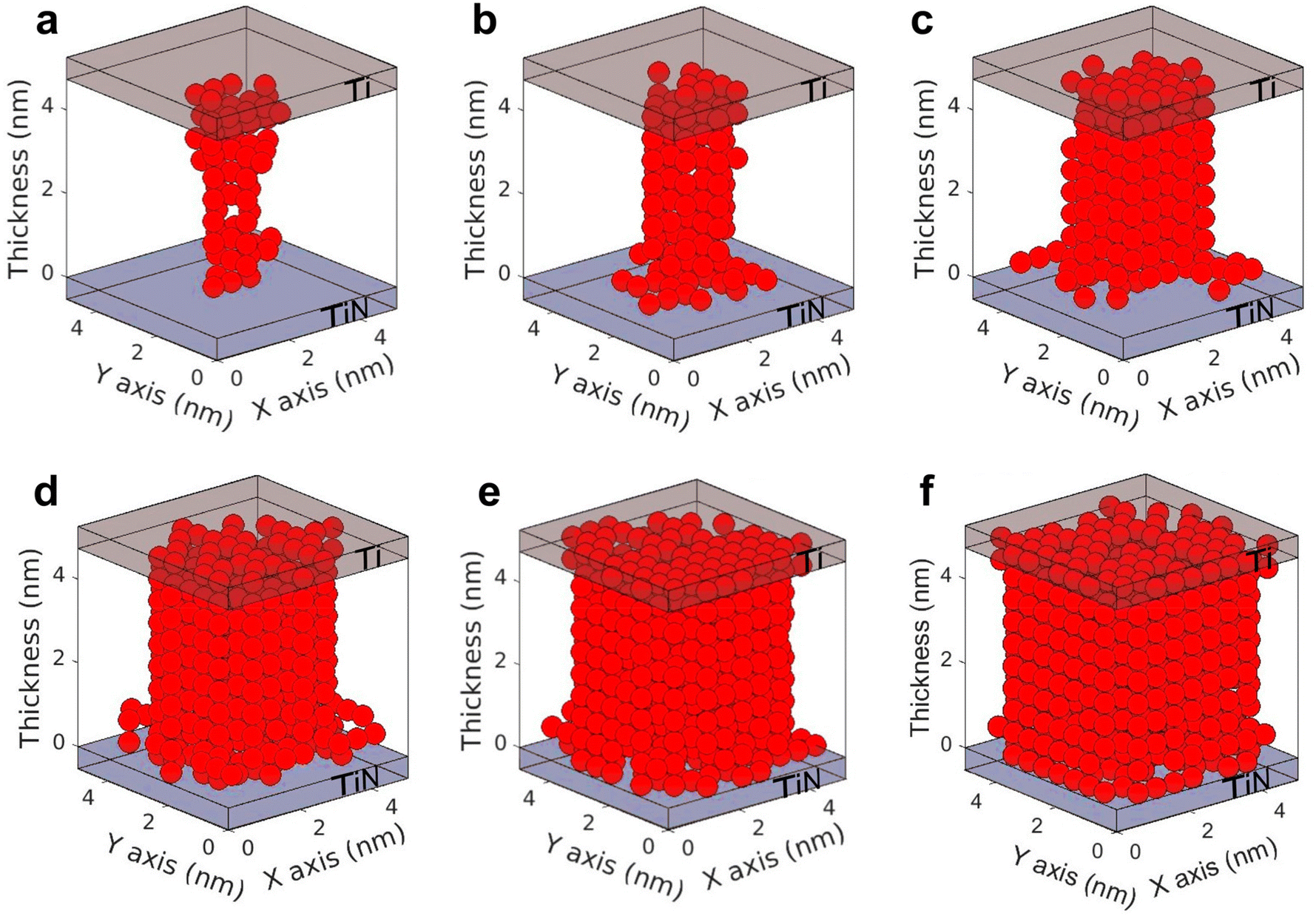 | ||
| Fig. 3 Plot of the oxygen vacancies in the simulation domain (corresponding to the dielectric) of fully-formed CFs in simulated devices with a conductance that corresponds to the 6 distinct experimental LRS obtained with ISPVA: (a) LRS1, (b) LRS2, (c) LRS3, (d) LRS4, (e) LRS5, (f) LRS6. | ||
Slight variations of the electrical conductivity were employed (<15%) to tune some of the LRS levels with the simulator due to the difficulty to exactly form a CF that corresponds to the device conductance levels fixed with the ISPVA methodology. Once the LRS conductance levels were fit, each individual device underwent a simulation period of 24 hours as it was the case in the experimental procedure. An illustration of the results for a device in the LRS3, exhibiting the CF evolution at all time points experimentally considered (0 min, 10 min, 20 min, 30 min, 40 min, 50 min, 1 h, 2 h, 5 h, 8 h, 24 h), is presented in Fig. 4. Minimal variations are observed along the simulation time, indicating the robustness of the filament structure which aligns with the experimental results. Additionally, Fig. 4l depicts the current versus time plot, demonstrating a stable current level throughout the simulation period.
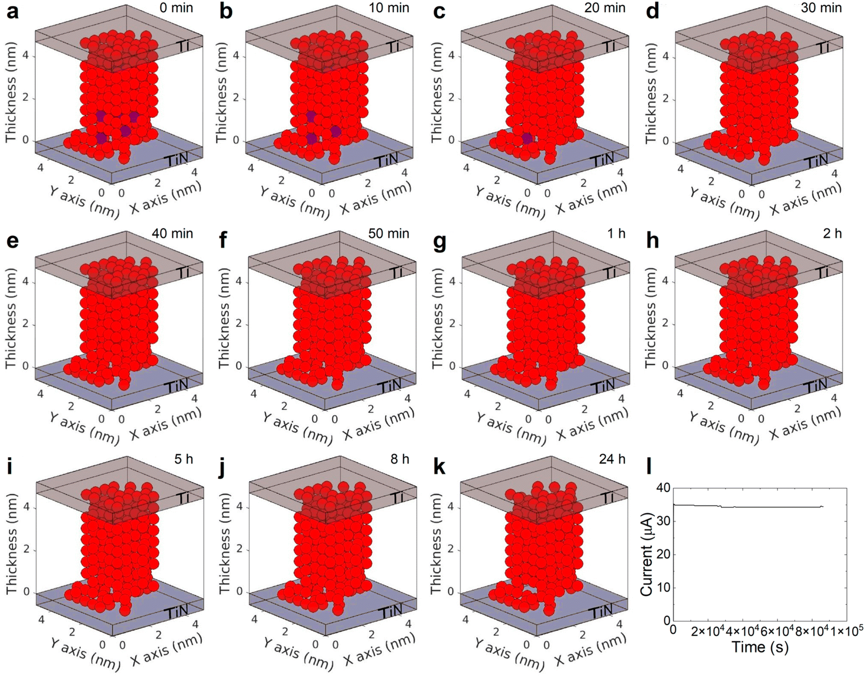 | ||
| Fig. 4 (a–k) kMC simulated CF evolution for a device in the LRS3. Prior to the test, an initialization simulation is performed to create a CF. As can be seen in the simulated experiment, a very slight morphological CF degradation is produced over time. Red balls depict oxygen vacancies and purple ones denote grid points where both an oxygen vacancy and an oxygen ion (not recombined) are present. (l) Read-out current versus time obtained during the simulation. | ||
It is worth emphasizing that the read-out voltage is maintained at a low level (0.2 V), ensuring minimal influence on the device conductance and, therefore, on the CF shape. The experimental measurements and the simulation analysis describe a scenario with two competing thermally-driven phenomena:34 generation of new oxygen vacancy-ion pairs and the injection of oxygen ions from the Ti layer into the dielectric, also taking into account subsequent oxygen ion diffusion and their potential recombination with existing oxygen vacancies. Although titanium shows a high affinity for oxygen,17 oxygen ions can be released back into the dielectric layer. When the injection of oxygen ions into the dielectric predominates, then the CF degradation process takes place and its progressive rupture occurs. This may lead to a transition from the programmed LRS to a less conductive LRS.
Fig. 5 provides a comparative illustration of the cumulative distribution functions (CDF) of the read-out current calculated for the 128 devices, specifically for the LRS4. The graph showcases panels a to k, representing the experimental and simulated data across all distinct temporal points. Simulated data reproduce reasonably well the experimental measurements, taking into consideration the stochasticity in the experimental data. Furthermore, Fig. 5l shows the plot of all the temporal CDFs considered for a complete analysis.
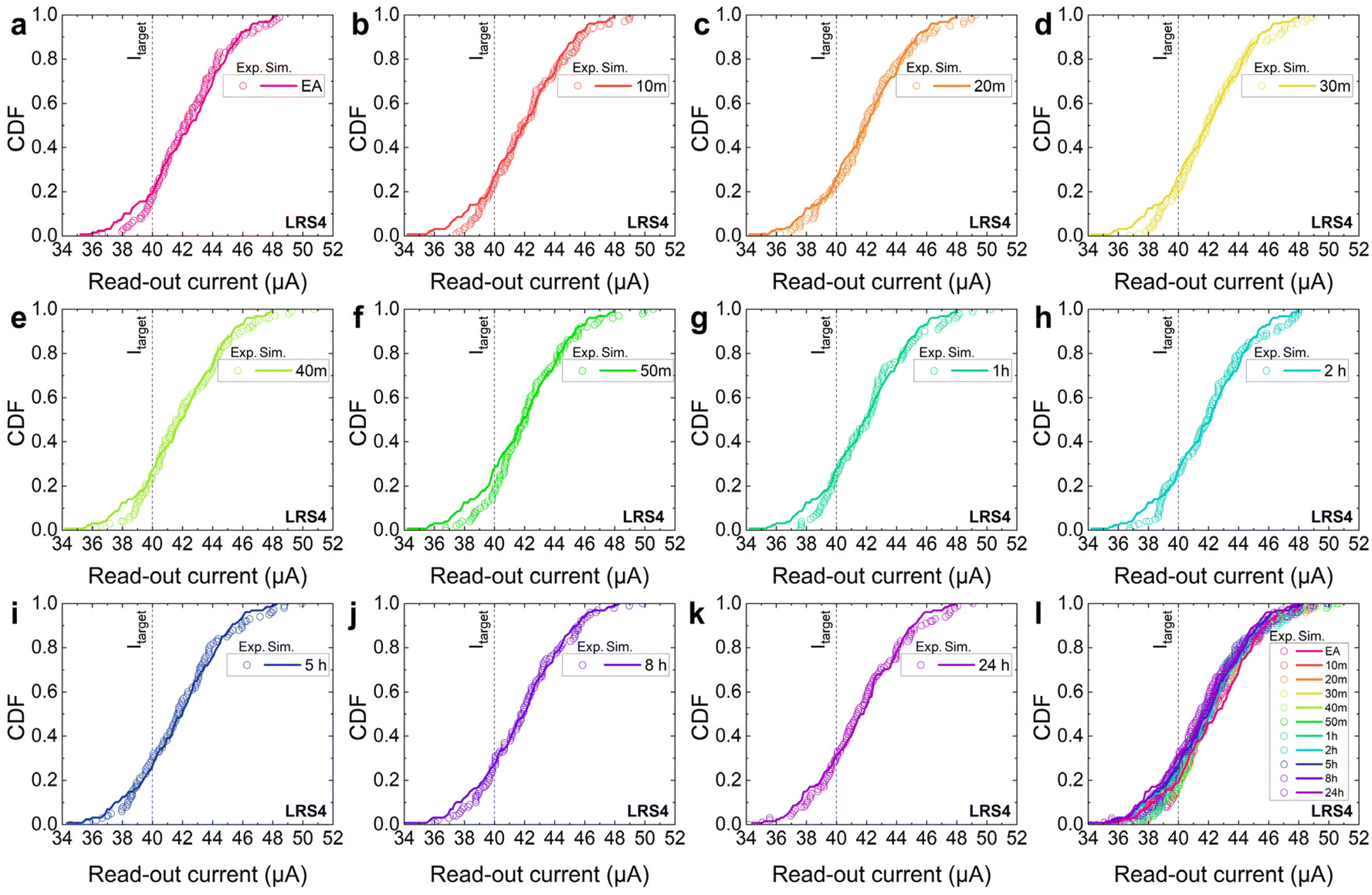 | ||
| Fig. 5 Comparative representation of the read-out current CDFs, corresponding to LRS4, obtained from experimental (dots) and simulated (lines) data for a sample set comprising 128 distinct devices. Eleven time steps were considered: (a) EA (0 min), (b) 10 min, (c) 20 min, (d) 30 min, (e) 40 min, (f) 50 min, (g) 1 h, (h) 2 h, (i) 5 h, (j) 8 h, (k) 24 h, (l) all the data plotted together. | ||
Fig. 6 shows the comparisons of the CDFs representing the read-out current for both the experimental and simulated data across LRS1 to LRS6. The observed drift of the curves towards lower currents, at longer times, corresponds to a CF degradation that could mean an operational failure, which is determined when the read-out current falls below the predefined current target levels of LRS1–LRS6, respectively. It is clear from the experimental data, and well represented by the simulations, that the larger is the conductivity of the LRS the lower the degradation suffered by the device, in agreement with previous retention studies.26,56
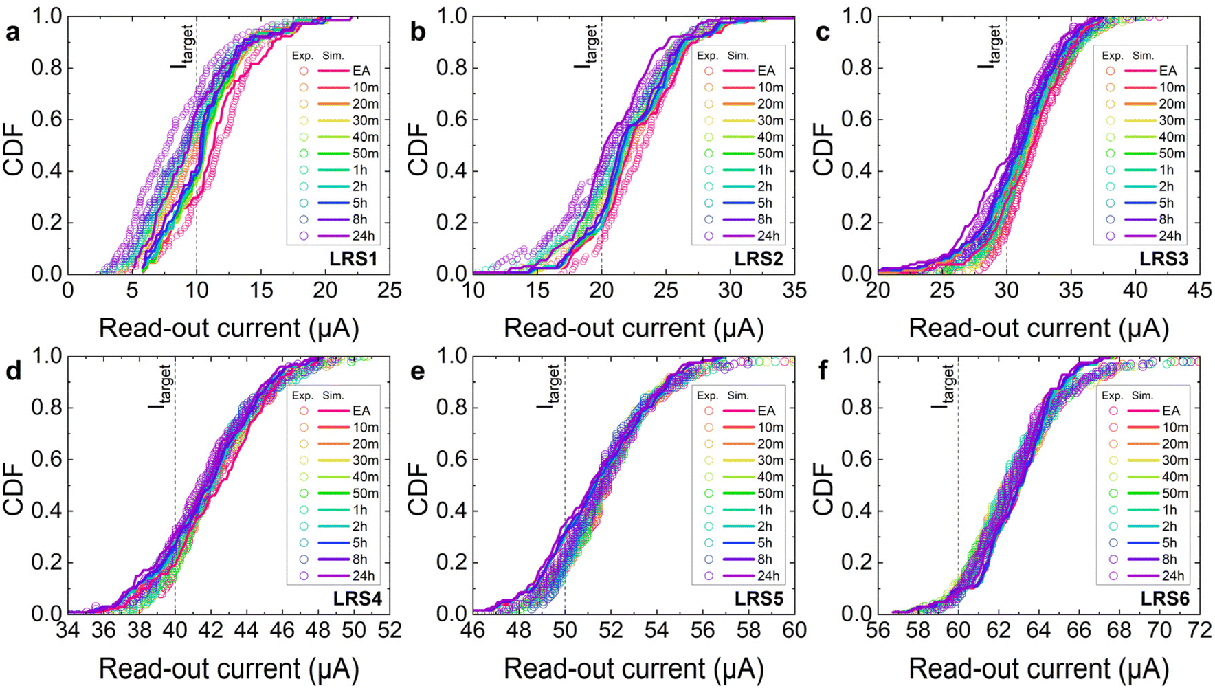 | ||
| Fig. 6 Comparative representation of the read-out current CDFs obtained from experimental (dots) and simulated (lines) data in a sample set comprising 128 distinct devices, covering eleven time steps: EA (0 min), 10 min, 20 min, 30 min, 40 min, 50 min, 1 h, 2 h, 5 h, 8 h, and 24 h. The analysis encompasses 6 distinct LRS: (a) LRS1, (b) LRS2, (c) LRS3, (d) LRS4, (e) LRS5, (f) LRS6. | ||
Fig. 7 illustrates the CDF of the percentages of devices showing failure over time in both experiments and simulations. A failure is determined when the read-out current measured in one device goes below the threshold employed to define a certain LRS level during programming. Noting that, despite discrepancies arising from the potential misrepresentation of the simulated filament relative to the real scenario, devices with larger CF radii exhibit fewer instances of failure, indicating slower CF degradation. These CDFs are supposed to present positive growth over time, however, occasional drops are observed within the curves, despite the overall increasing trend. These fluctuations are attributed to the interplay between CF degradation and regeneration mechanisms which impacts the stability and conductance over time, as outlined previously.
 | ||
| Fig. 7 CDF of the failure rate as a function of the time observed in a sample of 128 individual devices, categorized into 6 distinct low resistance states (LRS1–LRS6) for the experimental data (squares) and simulations (circles). | ||
To gain a deeper understanding on the morphological properties of the different LRSs, some specific parameters have been extracted from the simulation. To quantify the CF compactness evolution, we follow an approach that detects two-dimensional (2D) percolation paths within the 3D structure. This is performed by a plane-by-plane analysis along the X and Y axes, within the simulation domain (the Z coordinate corresponds to the direction perpendicular to the dielectric/electrode interface). The determination of percolation paths is facilitated by adapting the Hoshen–Kopelman algorithm57 to work in 2D within these planes. The values are employed to characterize the compactness of the CF and facilitate comparisons between 3D and 2D simulation methodologies.34 It is worth noting that even in the absence of 2D percolation paths, it is still possible that a 3D percolation path may exist as consequence to lateral connections between distinct planes. A lower amount of 2D percolation paths indicates less CF compactness, and, therefore, CF instability. The evolution of the number of 2D percolation paths throughout the simulation time is shown in Fig. 8. Notice that for higher CF radii, the number of 2D percolation paths exhibits greater stability over time.58
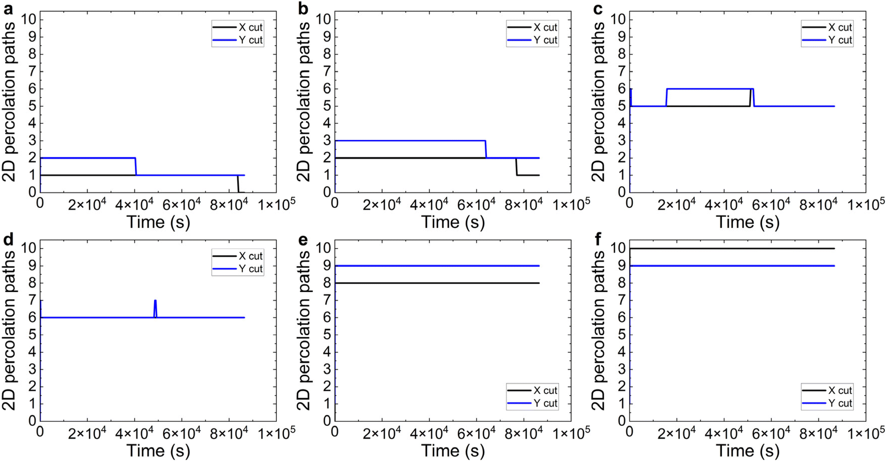 | ||
| Fig. 8 Number of two-dimensional percolation paths within the CF structure for the 6 distinct LRSs employed in our study: (a) LRS1, (b) LRS2, (c) LRS3, (d) LRS4, (e) LRS5, and (f) LRS6. | ||
Furthermore, the amount of oxygen vacancies surrounded by a specific number of neighboring vacancies is depicted in Fig. 9. In our analysis, the maximum number of neighbors is assumed to be six, excluding diagonal connections.10,34 Consequently, classical cluster considerations, which only account for neighbors in the vertical and horizontal direction are applied.
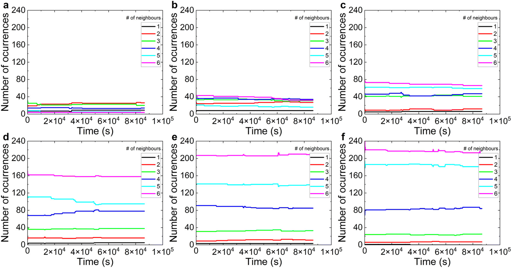 | ||
| Fig. 9 Time evolution of the number of oxygen vacancies with a determined number of neighbors in the CF for the 6 different conductance levels under consideration: (a) LRS1, (b) LRS2, (c) LRS3, (d) LRS4, (e) LRS5, and (f) LRS6. | ||
A higher occurrence of five and six neighboring vacancies corresponds to a high CF compactness (consequently, a low CF ohmic resistance for the same CF volume). As the CF radius rises, corresponding to a higher conductance level, the frequency of five and six neighbor occurrences increases (i.e., a higher CF compactness).
The examination of the CF density yields intriguing insights, see Fig. 10a. To assess this parameter, we utilize ellipses that best encapsulate the CF within each layer of the simulation domain, spanning from the bottom to the top electrode. The focal points of these ellipses are determined by using a clustering algorithm. By obtaining an ellipse for each layer, it is possible to assess the volume of the CF and, therefore, the density. See also that Fig. 10a sheds light on the interpretation of the device conductance degradation over time. This degradation is also evident in the reduction of the number of 2D percolated layers, as illustrated in some panels of Fig. 8. In general, these findings indicate a decrease in the CF compactness and a corresponding increase in its ohmic resistance. This degradation occurs due to oxygen injection coming from the top electrode into the simulation domain and the subsequent recombination with vacancies. Non-relevant short-term increases observed in the figure result from the generation of new Anti-Frenkel pairs.
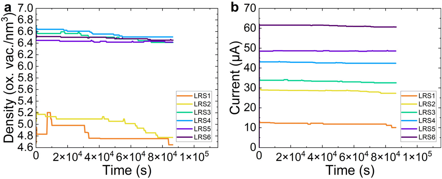 | ||
| Fig. 10 (a) Comparison of CF density for a particular device over time, for the 6 different conductance levels under consideration, (b) simulated read-out current of one particular device as a function of time for the multilevel operation under study: LRS1, LRS2, LRS3, LRS4, LRS5, and LRS6. | ||
The observed discrepancy in density between LRS1 and LRS2, compared to LRS3, LRS4, LRS5, and LRS6, can be attributed to variations in the formation and structural characteristics of the CF across different device conductance levels. During the initial stages of CF formation in LRS1 and LRS2, the CFs exhibit relatively lower densities due to the limited growth. As the device undergoes further writing operations, the CFs in LRS3, LRS4, LRS5, and LRS6 experience additional growth and stabilization, leading to denser CFs. This phenomenon explains Fig. 7, where a CF degradation is expected and the consequent failure rate increases (mostly at LRS1 and LRS2); occasionally a failure rate decrease is also observed (due to the inherent stochasticity of the RS). Regarding this, it is important to refer to Fig. 6, where the target currents for each LRS are shown which are the following: 10 μA for LRS1, 20 μA for LRS2, 30 μA for LRS3, 40 μA for LRS4, 50 μA for LRS5, and 60 μA for LRS6. These values are critical in defining the different LRS and understanding the stability and reliability of the CFs in each state. The higher target currents for LRS4, LRS5, and LRS6 correspond to the more stable and denser CFs, which explains the lower failure rates observed in these states compared to LRS1 and LRS2.
See also Fig. 10b, where it is shown the variation of current values for LRS1 to LRS6 as a function of time. Note that the higher current levels for filaments with similar densities result from the larger sizes of the filaments. Notably, the depicted currents exhibit remarkable stability over time, with only a slight decrease observed across the duration of the simulation. This consistent current behavior underscores the robustness and reliability of the devices under investigation. See a higher current reduction with time for LRS1 and LRS2, which corresponds to less compact CFs as expected (Fig. 10a).
Notice that the kMC simulator is useful to shed light on our devices RS features. In addition, the simulation tool can be of great value if non-homogeneous dielectrics are employed, e.g. using multilayers, doped oxides, etc. The CF compactness can be employed to monitor conductance drift features and the accuracy of multilevel strategies for device operation on the neuromorphic computing arena.
5. Conclusions
The retention characteristics of VCM devices have been investigated through a combination of experimental measurements and 3D kMC simulations. It has been demonstrated experimentally that retention properties remain stable with just a slight degradation over time, and this behavior has been accurately replicated through simulations. The interplay between the generation of new oxygen vacancies and their subsequent recombination with oxygen ions is critical in establishing the retention performance of the technology under study. Some valuable insights provided by the kMC simulator, such as the percolation paths formation as well as the CF compactness and density, have been studied in detail. The analysis highlighted that the devices with wider CFs formed (corresponding to the conductance levels LRS4 to LRS6) exhibited higher stability and lower failure rates compared to those with narrower CFs (LRS1 to LRS3), emphasizing the importance of controlling and modeling CF dynamics to enhance device reliability.Author contributions
The preparation of the samples was done by K. D. S. R. The experimental measurements were carried out by A. B. The kMC simulations were performed by D. M., S. A. and J. B. R. The design of the manuscript was performed by D. M., E. P., J. B. R. All authors have participated in the writing and revision of the manuscript and have given approval to the final version of the manuscript.Data availability
The datasets generated and/or analyzed during the current study are available from the corresponding author on reasonable request.Conflicts of interest
The authors declare no competing interest.Appendix
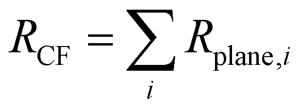
The conduction for a stable percolation path is modeled by considering ohmic conduction in the filament, the Maxwell resistances, and series resistance, all arranged in series.59To calculate the ohmic conduction in the filament, we first divide the conductive filament cluster into layers along the z-axis (the direction of the current). For each plane, we account for the number of oxygen vacancies (nv0) within the cluster. The resistance of each plane is then calculated using the following equation:

• ρ is the electrical resistivity.
• Splane and SVo are the transverse section of the cluster in that plane and per oxygen vacancy respectively.
• h is the separation between planes.
• αT = 0.022 K−1 is the temperature coefficient of the conductivity.
• T0 is the reference temperature.
• Tm is the mean temperature of the plane.
The total resistance of the conductive filament (CF) can then be calculated by summing the resistances of all planes:
Acknowledgements
The authors thank the support of the Federal Ministry of Education and Research of Germany under Grant 16ME0092. They also acknowledge project PID2022-139586NB-C44 funded by MCIN/AEI/10.13039/501100011033 and FEDER, EU. The ASCENT+ Access to European Infrastructure supported Samuel Aldana Delgado for Nanoelectronics Program, funded through the EU Horizon Europe programme, grant no 871130.References
- M. Lanza, A. Sebastian, W. D. Lu, M. L. Gallo, M.-F. Chang and D. Akinwande, et al., Memristive technologies for data storage, computation, encryption, and radio-frequency communication, Science, 2022, 376, eabj9979, DOI:10.1126/science.abj9979.
- N. Wainstein, G. Adam, E. Yalon and S. Kvatinsky, Radiofrequency Switches Based on Emerging Resistive Memory Technologies - A Survey, Proc. IEEE, 2021, 109, 77–95, DOI:10.1109/jproc.2020.3011953.
- Z. Wei, Y. Katoh, S. Ogasahara, Y. Yoshimoto, K. Kawai and Y. Ikeda, et al., True random number generator using current difference based on a fractional stochastic model in 40 nm embedded ReRAM, 2016. DOI:10.1109/iedm.2016.7838349.
- R. Romero-Zaliz, A. Cantudo, E. Perez, F. Jimenez-Molinos, C. Wenger and J. B. Roldan, An Analysis on the Architecture and the Size of Quantized Hardware Neural Networks Based on Memristors, Electronics, 2021, 10, 3141, DOI:10.3390/electronics10243141.
- E. P.-B. Quesada, R. Romero-Zaliz, E. Pérez, M. K. Mahadevaiah, J. Reuben and M. A. Schubert, et al., Toward Reliable Compact Modeling of Multilevel 1T-1R RRAM Devices for Neuromorphic Systems, Electronics, 2021, 10, 645, DOI:10.3390/electronics10060645.
- F. Aguirre, A. Sebastian, M. L. Gallo, W. Song, T. Wang and J. J. Yang, et al., Hardware implementation of memristor-based artificial neural networks, Nat. Commun., 2024, 15, 1974, DOI:10.1038/s41467-024-45670-9.
- D. J. Wouters, S. Menzel, J. a. J. Rupp, T. Hennen and R. Waser, On the universality of the I–V switching characteristics in non-volatile and volatile resistive switching oxides, Faraday Discuss., 2019, 213, 183–196, 10.1039/c8fd00116b.
- C. Funck and S. Menzel, Comprehensive Model of Electron Conduction in Oxide-Based Memristive Devices, ACS Appl. Electron. Mater., 2021, 3, 3674–3692, DOI:10.1021/acsaelm.1c00398.
- F. Pan, S. Gao, C. Chen, C. Song and F. Zeng, Recent progress in resistive random access memories: Materials, switching mechanisms, and performance, Mater. Sci. Eng., R, 2014, 83, 1–59, DOI:10.1016/j.mser.2014.06.002.
- S. Aldana, P. García-Fernández, R. Romero-Zaliz, M. B. González, F. Jiménez-Molinos and F. Gómez-Campos, et al., Resistive switching in HfO2 based valence change memories, a comprehensive 3D kinetic Monte Carlo approach, J. Phys. D: Appl. Phys., 2020, 53, 225106, DOI:10.1088/1361-6463/ab7bb6.
- X. Guan, S. Yu and H.-s. P. Wong, On the Switching Parameter Variation of Metal-Oxide RRAM—Part I: Physical Modeling and Simulation Methodology, IEEE Trans. Electron Devices, 2012, 59, 1172–1182, DOI:10.1109/ted.2012.2184545.
- A. Padovani, L. Larcher, O. Pirrotta, L. Vandelli and G. Bersuker, Microscopic Modeling of HfOx RRAM Operations: From Forming to Switching, IEEE Trans. Electron Devices, 2015, 62, 1998–2006, DOI:10.1109/ted.2015.2418114.
- A. Padovani, D. Z. Gao, A. L. Shluger and L. Larcher, A microscopic mechanism of dielectric breakdown in SiO2 films: An insight from multi-scale modeling, J. Appl. Phys., 2017, 121, 155101, DOI:10.1063/1.4979915.
- B. Butcher, G. Bersuker, D.C Gilmer, L. Larcher, A. Padovani and L. Vandelli, et al., Connecting the physical and electrical properties of Hafnia-based RRAM, 2013. DOI:10.1109/iedm.2013.6724682.
- Y. Zhao, P. Huang, Z. Chen, C. Liu, H. Li and B. Chen, et al., Modeling and Optimization of Bilayered TaOxRRAM Based on Defect Evolution and Phase Transition Effects, IEEE Trans. Electron Devices, 2016, 63, 1524–1532, DOI:10.1109/ted.2016.2532470.
- F. M. Puglisi, L. Larcher, A. Padovani and P. Pavan, Bipolar Resistive RAM Based on HfO2: Physics, Compact Modeling, and Variability Control, IEEE J. Emerg. Sel. Topics Circuits Syst., 2016, 6, 171–184, DOI:10.1109/jetcas.2016.2547703.
- S. Dirkmann, J. Kaiser, C. Wenger and T. Mussenbrock, Filament Growth and Resistive Switching in Hafnium Oxide Memristive Devices, ACS Appl. Mater. Interfaces, 2018, 10, 14857–14868, DOI:10.1021/acsami.7b19836.
- E. Abbaspour, S. Menzel, A. Hardtdegen, S. Hoffmann-Eifert and C. Jungemann, KMC Simulation of the Electroforming, Set and Reset Processes in Redox-Based Resistive Switching Devices, IEEE Trans. Nanotechnol., 2018, 17, 1181–1188, DOI:10.1109/tnano.2018.2867904.
- M. Kaniselvan, M. Luisier and M. Mladenović, An Atomistic Model of Field-Induced Resistive Switching in Valence Change Memory, ACS Nano, 2023, 17, 8281–8292, DOI:10.1021/acsnano.2c12575.
- G. Bersuker, D. C. Gilmer, D. Veksler, P. Kirsch, L. Vandelli and A. Padovani, et al., Metal oxide resistive memory switching mechanism based on conductive filament properties, J. Appl. Phys., 2011, 110, 124518, DOI:10.1063/1.3671565.
- L. Larcher, A. Padovani and L. Vandelli, A simulation framework for modeling charge transport and degradation in high-k stacks, J. Comput. Electron., 2013, 12, 658–665, DOI:10.1007/s10825-013-0526-z.
- D. Ielmini and R. Waser, Resistive Switching: From Fundamentals of Nanoionic Redox Processes to Memristive Device Applications, Wiley-VCH, 2015. DOI:10.1002/9783527680870.
- A. Fantini, L. Goux, R. Degraeve, D. Wouters, P. Raghavan and G. S. Kar, et al., Intrinsic switching variability in HfO2 RRAM: A theoretical and experimental study, International Memory Workshop, 2013, pp. 30–33 Search PubMed.
- A. Grossi, C. Zambelli, P. Olivo, E. Nowak, G. Molas and J. F. Nodin, et al., Cell-to-Cell Fundamental Variability Limits Investigation in OxRRAM Arrays, IEEE Electron Device Lett., 2018, 39, 27–30, DOI:10.1109/led.2017.2774604.
- A. Fantini, G. Gorine, R. Degraeve, L. Goux, C. Y. Chen and A. Redolfi, et al., Intrinsic program instability in HfO2 RRAM and consequences on program algorithms, 2015. DOI:10.1109/iedm.2015.7409648.
- E. Perez, C. Zambelli, M. K. Mahadevaiah, P. Olivo and C. Wenger, Toward Reliable Multi-Level Operation in RRAM Arrays: Improving Post-Algorithm Stability and Assessing Endurance/Data Retention, IEEE J. Electron Devices Soc., 2019, 7, 740–747, DOI:10.1109/jeds.2019.2931769.
- L. Gao, Q. Ren, J. Sun, S.-T. Han and Y. Zhou, Memristor modeling: challenges in theories, simulations, and device variability, J. Mater. Chem. C, 2021, 9, 16859–16884, 10.1039/d1tc04201g.
- S. Clima, B. Govoreanu, M. Jurczak and G. Pourtois, HfOx as RRAM material – First principles insights on the working principles, Microelectron. Eng., 2014, 120, 13–18, DOI:10.1016/j.mee.2013.08.002.
- Z. Jiang, Y. Wu, S. Yu, L. Yang, K. Song and Z. Karim, et al., A Compact Model for Metal–Oxide Resistive Random Access Memory With Experiment Verification, IEEE Trans. Electron Devices, 2016, 63, 1884–1892, DOI:10.1109/ted.2016.2545412.
- P. Huang, X. Y. Liu, B. Chen, H. T. Li, Y. J. Wang and Y. X. Deng, et al., A Physics-Based Compact Model of Metal-Oxide-Based RRAM DC and AC Operations, IEEE Trans. Electron Devices, 2013, 60, 4090–4097, DOI:10.1109/ted.2013.2287755.
- P. Huang, D. Zhu, S. Chen, Z. Zhou, Z. Chen and B. Gao, et al., Compact Model of HfOX-Based Electronic Synaptic Devices for Neuromorphic Computing, IEEE Trans. Electron Devices, 2017, 64, 614–621, DOI:10.1109/ted.2016.2643162.
- R. Picos, J. B. Roldan, M. M. A. Chawa, F. Jimenez-Molinos and E. Garcia-Moreno, A physically based circuit model to account for variability in memristors with resistive switching operation, 2016. DOI:10.1109/dcis.2016.7845383.
- J. B. Roldán, G. González-Cordero, R. Picos, E. Miranda, F. Palumbo and F. Jiménez-Molinos, et al., On the Thermal Models for Resistive Random Access Memory Circuit Simulation, Nanomaterials, 2021, 11, 1261, DOI:10.3390/nano11051261.
- S. Aldana, E. Pérez, F. Jiménez-Molinos, C. Wenger and J. B. Roldán, Kinetic Monte Carlo analysis of data retention in Al:HfO2-based resistive random access memories, Semicond. Sci. Technol., 2020, 35, 115012, DOI:10.1088/1361-6641/abb072.
- S. Aldana and H. Zhang, Unravelling the Data Retention Mechanisms under Thermal Stress on 2D Memristors, ACS Omega, 2023, 8, 27543–27552, DOI:10.1021/acsomega.3c03200.
- N. Raghavan, D. D. Frey, M. Bosman and K. L. Pey, Statistics of retention failure in the low resistance state for hafnium oxide RRAM using a Kinetic Monte Carlo approach, Microelectron. Reliab., 2015, 55, 1422–1426, DOI:10.1016/j.microrel.2015.06.090.
- A. Baroni, A. Glukhov, E. Perez, C. Wenger, D. Ielmini and P. Olivo, et al., Low Conductance State Drift Characterization and Mitigation in Resistive Switching Memories (RRAM) for Artificial Neural Networks, IEEE Trans. Device Mater. Reliab., 2022, 22, 340–347, DOI:10.1109/tdmr.2022.3182133.
- B. Traore, P. Blaise, E. Vianello, H. Grampeix, S. Jeannot and L. Perniola, et al., On the Origin of Low-Resistance State Retention Failure in HfO2-Based RRAM and Impact of Doping/Alloying, IEEE Trans. Electron Devices, 2015, 62, 4029–4036, DOI:10.1109/ted.2015.2490545.
- M. K. Mahadevaiah, M. Lisker, M. Fraschke, S. Marschmeyer, D. Schmidt and C. Wenger, et al., (Invited) Optimized HfO2-Based MIM Module Fabrication for Emerging Memory Applications, Meeting Abstracts/Meeting Abstracts (Electrochemical Society CD-ROM), 2019, MA2019-02, 1194. DOI:10.1149/ma2019-02/25/1194.
- E. Pérez, M. K. Mahadevaiah, C. Zambelli, P. Olivo and C. Wenger, Characterization of the interface-driven 1st Reset operation in HfO2-based 1T1R RRAM devices, Solid-State Electron., 2019, 159, 51–56, DOI:10.1016/j.sse.2019.03.054.
- S. Liu, J. Zeng, Z. Wu, H. Hu, A. Xu and X. Huang, et al., An ultrasmall organic synapse for neuromorphic computing, Nat. Commun., 2023, 14, 7655, DOI:10.1038/s41467-023-43542-2.
- S. Liu, X. Zhong, Y. Li, B. Guo, Z. He and Z. Wu, et al., A Self–Oscillated Organic Synapse for In–Memory Two–Factor Authentication, Adv. Sci., 2024, 11 DOI:10.1002/advs.202401080.
- J. Guy, G. Molas, P. Blaise, M. Bernard, A. Roule and G. L. Carval, et al., Investigation of Forming, SET, and Data Retention of Conductive-Bridge Random-Access Memory for Stack Optimization, IEEE Trans. Electron Devices, 2015, 62, 3482–3489, DOI:10.1109/ted.2015.2476825.
- A. F. Voter, Introduction to the kinetic Monte Carlo method. Springer eBooks, 2007, pp. 1–23. DOI:10.1007/978-1-4020-5295-8_1.
- N. D. Lu, Z. W. Zong, P. X. Sun, L. Li, Q. Liu and H. B. Lv, et al., Thermal effect and Compact model in three-dimensional (3D) RRAM arrays, 2016. DOI:10.1109/SISPAD.2016.7604686.
- L. Vandelli, A. Padovani, L. Larcher, G. Bersuker, J. Yum and P. Pavan, A physics-based model of the dielectric breakdown in HfO2 for statistical reliability prediction, 2011. DOI:10.1109/irps.2011.5784582.
- B. Gao, J. F. Kang, H. W. Zhang, B. Sun, B. Chen and L. F. Liu, et al., Oxide-based RRAM: Physical based retention projection, 2010. DOI:10.1109/essderc.2010.5618200.
- Z. Gao, S. Yu and W. Liu, et al., Oxide-based RRAM: Uniformity improvement using a new material-oriented methodology, Symposium on VLSI Technology, 2009, pp. 30–31 Search PubMed.
- A. Padovani, L. Larcher, G. Bersuker and P. Pavan, Charge Transport and Degradation in HfO2 and HfOx Dielectrics, IEEE Electron Device Lett., 2013, 34, 680–682, DOI:10.1109/led.2013.2251602.
- M. Rao, H. Tang, J. Wu, W. Song, M. Zhang and W. Yin, et al., Thousands of conductance levels in memristors integrated on CMOS, Nature, 2023, 615, 823–829, DOI:10.1038/s41586-023-05759-5.
- R. Govindaraj, C. S. Sundar and R. Kesavamoorthy, Atomic scale study of oxidation of hafnium: Formation of hafnium core and oxide shell, J. Appl. Phys., 2006, 100, 084318, DOI:10.1063/1.2360148.
- S. R. Bradley, A. L. Shluger and G. Bersuker, Electron-Injection-Assisted Generation of Oxygen Vacancies in MonoclinicHfO2, Phys. Rev. Appl., 2015, 4, 064008, DOI:10.1103/physrevapplied.4.064008.
- P. Rottländer, M. Hehn and A. Schuhl, Determining the interfacial barrier height and its relation to tunnel magnetoresistance, Phys. Rev. B: Condens. Matter Mater. Phys., 2002, 65, 054422, DOI:10.1103/physrevb.65.054422.
- H. Schroeder, Poole-Frenkel-effect as dominating current mechanism in thin oxide films—An illusion?!, J. Appl. Phys., 2015, 117, 215103, DOI:10.1063/1.4921949.
- A. S. Foster, A. L. Shluger and R. M. Nieminen, Mechanism of Interstitial Oxygen Diffusion in Hafnia, Phys. Rev. Lett., 2002, 89, 225901, DOI:10.1103/physrevlett.89.225901.
- D. Ielmini, F. Nardi, C. Cagli and A. L. Lacaita, Size-Dependent Retention Time in NiO-Based Resistive-Switching Memories, IEEE Electron Device Lett., 2010, 31, 353–355, DOI:10.1109/led.2010.2040799.
- J. Hoshen and R. Kopelman, Percolation and cluster distribution. I. Cluster multiple labeling technique and critical concentration algorithm, Phys. Rev. B: Solid State, 1976, 14, 3438–3445, DOI:10.1103/physrevb.14.3438.
- S. Aldana, P. García-Fernández, R. Romero-Zaliz, F. Jiménez-Molinos, F. Gómez-Campos and J. B. Roldán, Analysis of conductive filament density in resistive random access memories: a 3D kinetic Monte Carlo approach, J. Vac. Sci. Technol., B: Nanotechnol. Microelectron.: Mater., Process., Meas., Phenom., 2018, 36, 062201, DOI:10.1116/1.5049213.
- S. Aldana, P. García-Fernández, A. Rodríguez-Fernández, R. Romero-Zaliz, M. B. González and F. Jiménez-Molinos, et al., A 3D kinetic Monte Carlo simulation study of resistive switching processes in Ni/HfO2/Si-n+-based RRAMs, J. Phys. D: Appl. Phys., 2017, 50, 335103, DOI:10.1088/1361-6463/aa7939.
| This journal is © The Royal Society of Chemistry 2024 |