
 Open Access Article
 This Open Access Article is licensed under a
 Creative Commons Attribution 3.0 Unported Licence
Quantitative photocurrent scanning probe microscopy on PbS quantum dot monolayers†
Florian
Küstner
a,
Harald
Ditlbacher
a,
Andreas
Hohenau
 a,
Dmitry N.
Dirin
bc,
Maksym
Kovalenko
bc and
Joachim R.
Krenn
*a
a,
Dmitry N.
Dirin
bc,
Maksym
Kovalenko
bc and
Joachim R.
Krenn
*a
aInstitute of Physics, University of Graz, 8010 Graz, Austria
bInstitute of Inorganic Chemistry, Department of Chemistry and Applied Biosciences, ETH Zürich, 8093 Zürich, Switzerland
cEmpa – Swiss Federal Laboratories for Materials Science and Technology, Laboratory for Thin Films and Photovoltaics, 8600 Dübendorf, Switzerland
First published on 16th August 2024
Abstract
Photoconductive atomic force microscopy can probe monolayers of PbS/perovskite quantum dots (QDs) with a contact area of 1–3 QDs in stable and reproducible acquisition conditions for I/V curves and photocurrent maps. From the measurements, quantitative values for the barrier height, built-in voltage, diffusion constant and ideality factor are deduced with high precision. The data analysis is based on modelling a superposition of the drift current of the photo-excited charges and a diffusion current across the interface barriers, providing physical insight into the underlying processes. Besides looking into PbS/perovskite on an indium tin oxide substrate, it is shown how the photocurrent is modified by changing either the QD ligand (to thiocyanate) or the substrate (to micro- and nanostructured gold). The dependence of the photocurrent on the light irradiance is found to follow a power law with an exponent of 0.64. Generally, quantitative measurements with high spatial resolution (on the single QD level) can provide significant insight into the processes in nanostructured hybrid optoelectronic components.
Introduction
Lead sulfide (PbS) colloidal quantum dots (QDs) are well known as stable and size-tunable broadband light absorbers and emitters in the red and near-infrared spectral regions.1 Due to their efficient photoelectric response and the relative ease of solution-based device fabrication, PbS QD photodetectors2–5 and photovoltaic cells6 have met considerable interest and record figures of merit were demonstrated.For the required electrical conductivity in QD ensembles, the long organic ligands used during synthesis have to be exchanged,7,8 resulting in efficient charge transfer, improved device performance9 and reduced barriers and traps.10 A significant breakthrough for QD photodevices was the phase-transfer (solution-phase) ligand exchange technique.11,12 This method ensures complete ligand exchange and simplifies by-product separation due to the uniform liquid reaction medium around the QDs. It also facilitates the single-step deposition of compact and crack-free QD films from solution-based inks, where QDs are pre-coated with the desired ligands, saving considerable time and materials. However, it requires a careful selection of ligands and solvents for exchange, storage, and deposition. Various ligands have been utilized for QD inks, with halides and metal halide complex anions being the most common to ensure good passivation of surface states.13–15 Recently, some of us identified 2,6-difluoropyridine as an effective solvent for QDs capped with small inorganic ligands, maintaining PbS QD ink stability for over 20 months and enabling the easy deposition of high-quality films.16,17
For the optoelectronic characterization of QDs, small ensembles and thin films thereof and in particular as part of hybrid nanostructures, experimental techniques with adequate spatial resolution are needed. To study light/exciton coupling and the resulting photocurrents this is to some extent met by scanning photocurrent microscopy that relies on a scanned laser focus locally generating charge.18–20 Overcoming the optical resolution limit and exploiting local conductance measurements with nanoscale resolution is however only provided by scanning probe techniques with an electric detection channel, such as conductive atomic force microscopy (cAFM)21 or, when light-induced currents are involved, photocurrent atomic force microscopy (pcAFM).22,23
With pcAFM, photocurrents from thin film solar cells were probed with a spatial resolution of 20 nm.24 High resolution was key to look into nanoscale percolation charge pathways in silicon heterojunction cells.25 On perovskite films, the method revealed the role of ion migration.26 On the other hand, depending on the type of sample and/or probe tip, contact issues or tip-induced effects were found to hamper or impede quantitative measurements with pcAFM.22,27
In this letter, we apply pcAFM with a PtIr coated silicon tip to probe monolayers of PbS QDs with an ultrathin perovskite shell. We acquire stable and reproducible I/V curves and photocurrent maps and retrieve a quantitative picture of the barrier heights at the QD/electrode interfaces and the bias-dependence of charge generation. The photocurrent dependence on the exciting light irradiance is measured by probing a few QDs only, yielding consistent power laws with exponents that are however strongly dependent on the underlying substrate (indium tin oxide, gold).
Experimental
The measurements were done with a pcAFM installed on an inverted optical microscope, the illumination setup is sketched schematically in Fig. 1(a). PtIr coated silicon probes (Bruker SCM-PIT-V2) were operated in either contact mode at a contact force of 0.6 nN or in peak force tapping mode.28 In the latter, for each interaction point on the sample the tip follows a full approach trajectory with a modulation amplitude of 280 nm at a frequency of 800 Hz, up to a tip/sample interaction peak force of 10 nN. | ||
| Fig. 1 (a) Sketch of the pcAFM with a PtIr tip to probe QD layers. With a grounded tip, the bias is applied to the sample and the photocurrent is measured with an I/V amplifier. (b) Peak force tapping AFM image of a PbS/MAPbI3 QD layer edge with a measured step height of 3.8 ± 0.7 nm (averaged along the edge). | ||
With the tip on electric ground, the bias was applied to the sample. The photocurrent was measured with an I/V amplifier set to 1 nA V−1, a root mean square noise level of 55 fA and saturation levels of ±10 nA. The QD layers were reproducibly scanned with typical photocurrents in the range of sub-pA to tens of pA for applied bias voltages up to a few volt. We note that contact mode measurements were prone to tip-induced QD shifts resulting in streak features along the fast (horizontal) scan direction in the images, while peak force tapping images were free of this effect. Nevertheless, the contact mode can be advantageous in the case of low currents and structured sample surfaces. This is on one hand due to the reduced tip/sample contact time in peak force mode, resulting in about ten times smaller time-averaged currents than for contact measurements. On the other hand, the tapping frequency of 800 Hz calls for a trade-off of scan rate (and thus time) and obtainable spatial resolution, which is more challenging when stronger corrugated surfaces are to be followed.
The tip was positioned and kept in the center of a focused HeNe laser beam (wavelength 633 nm) while the sample was scanned. The laser was focused with either a 10×, 0.3 numerical aperture (N.A.) objective or a 60×, 1.4 N.A. oil immersion objective. For the individual experiments we list the laser power incident on the sample as well as the estimated peak irradiance at the position of the tip, with maximum values of 10 and 15 kW cm−2 for the 10× and 60× objectives, respectively (see the ESI, S1†). The lowest irradiances considered for I/V curves and current maps are 400 W cm−2 and 3 W cm−2, respectively, with the current observed for the latter being close to the detection limit of our system. These values correspond to an average time between the absorption of two consecutive photons by the same QD of about 1–100 μs, with typical relaxation times of exited charges in the nano- and picosecond regime. Therefore, we expect that our findings also hold for lower irradiances.
The experiments with the 10× objective were done with a closed sample chamber of 0.14 mL around the AFM tip that was floated with nitrogen at a rate of 1.3 mL min−1. In combination with the 60× objective the pcAFM was operated in ambient air while the applied bias was limited to 200 mV. Under these conditions, no sample deterioration due to scanning was observed.
The substrate for all samples was a glass slide coated with a few nm of conductive indium tin oxide (ITO). Before QD deposition, the ITO surface was exposed to an ambient air plasma. Gold micro- and nanostructures were fabricated on ITO/glass substrates by electron beam lithography. Therefore, a 100 nm thick poly(methyl methacrylate) thin film was exposed by the electron beam and chemically developed. Physical vapor deposition of approximately 1 nm of chromium and 40 nm of gold was followed by liftoff. After exposure to an ambient air plasma the QD films were deposited.
PbS QDs coated with an about 1 nm thick methylammonium lead iodide (MAPbI3) perovskite shell and an overall diameter of nominally 3.2 nm were synthesized as described before20 (see Methods). Monolayer films were deposited by spin coating 30 μL of a solution with 10 g L−1 in 2,6-difluoropyridine at 2000 rpm. The presence of a QD monolayer was confirmed by imaging an edge of the QD layer along a mechanically induced scratch using AFM, giving a step height of 3.8 ± 0.7 nm (Fig. 1(b)). As we thus deal with a QD monolayer, the substrate and the PtIr tip are bridged by only a few QDs, with the actual number determined by the tip geometry. We estimate the number of QDs contributing to the current in parallel to be between 1 and 17 (see the ESI, S2†), a range that we can further narrow to 1–3 in the course of data analysis. For additional measurements, we prepared PbS QDs capped with thiocyanate (SCN). Here, a step height of 10 ± 2 nm was measured for the spin coated film, indicative of three QD layers.
Results and discussion
An I/V curve acquired by statically positioning the tip on the QD monolayer (contact force 6 nN) and illuminating the sample through the 10× objective (laser power 8 μW, irradiance 0.4 kW cm−2) is plotted in Fig. 2(a). Up to a voltage of about ±1 V the current depends fairly linear on the bias, as also evidenced by the current dependencies for different irradiances in Fig. 2(b). For higher bias voltages up to ±5 V the I/V dependence is markedly nonlinear. Furthermore, we observe a somewhat asymmetric curve with a bias-offset V0 of −0.7 V.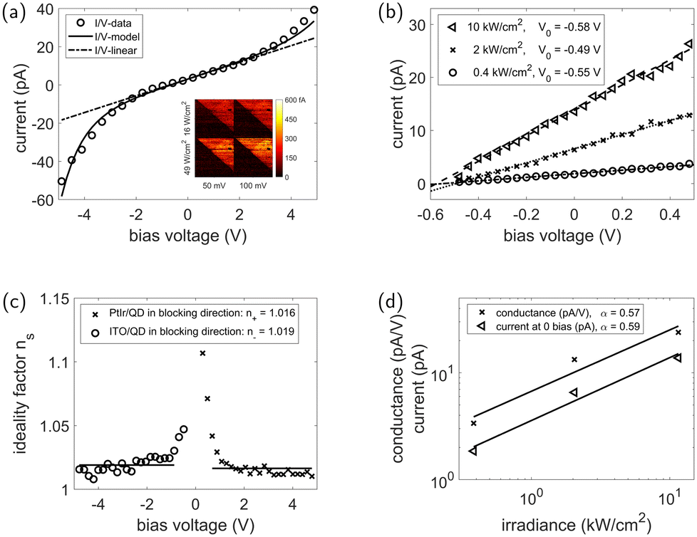 | ||
| Fig. 2 Voltage and irradiance dependencies of the photocurrent from a PbS/MAPbI3 QD monolayer measured by pcAFM. (a) I/V curve, the symbols show the data measured with a point contact force of 6 nN and a laser power of 8 μW (irradiance 0.4 kW cm−2) delivered through the 10× objective. Zero current is observed for a bias V0 of −0.7 V. The full and dash-dotted lines show the full modelled curve and its linear part only, respectively. The inset depicts four photocurrent maps of the same scan area half-covered (upper right) with the QD monolayer for bias voltages and irradiances as indicated. (b) I/V curves over a lower voltage range for irradiances of 0.4, 2 and 10 kW cm−2. The V0 values for the individual curves are indicated in the legend. (c) Voltage dependence of the ideality factor, the horizontal lines mark the initial guess of n+ = 1.016 and n− = 1.019. (d) Power law dependence of the conductance and the current at zero bias on the irradiance. | ||
Very similar I/V curves are observed at other positions on the QD film, however, the bias-offset was observed to vary up to 0.2 V with respect to the value noted here. For highlighting the reproducibility of the photocurrent measurement on the QD layers, the inset of Fig. 2(a) shows exemplarily four peak force tapping photocurrent images (at biases of 50 mV and 100 mV and different irradiances) of the same scan area half-covered with a PbS/MAPbI3 QD monolayer.
We model the measured I/V curve in Fig. 2(a) as the sum of a photocurrent and a thermionic emission contribution. For the photocurrent, the measured current values indicate that besides charges from QDs directly contacted by the AFM tip, a charge reservoir from neighboring QDs contributes to the signal. We address the photocurrent via Ohm's law and thus refer to it as drift current (first summand in eqn (1)). Charges due to thermionic emission across the energy barriers at the QD/electrode interfaces follow Fick's law, which we denote as a diffusion current (second summand in eqn (1)). The full model, which is described in detail in the ESI, S3,† is then given by:
 | (1) |
The additional diffusion current across the interface energy barrier is described by a thermionic emission model in blocking direction. The asymmetry in the system is taken into account by letting the ideality factor ns![[thin space (1/6-em)]](https://www.rsc.org/images/entities/char_2009.gif) 30 depend on the bias sign s = sign(Vext). In our description, the ideality factor is a phenomenological constant that models a linear dependency of the interface barrier height on the applied bias voltage. We note that Arya et al.31 discuss a physical model for colloidal QD junctions (in a planar layer structure) based on carrier transport mechanisms, deriving a fundamental relationship between the built-in voltage, the ideality factor and the interface barrier. Since this relationship cannot be made explicit, we do not take it into account in our model, but will address it later.
30 depend on the bias sign s = sign(Vext). In our description, the ideality factor is a phenomenological constant that models a linear dependency of the interface barrier height on the applied bias voltage. We note that Arya et al.31 discuss a physical model for colloidal QD junctions (in a planar layer structure) based on carrier transport mechanisms, deriving a fundamental relationship between the built-in voltage, the ideality factor and the interface barrier. Since this relationship cannot be made explicit, we do not take it into account in our model, but will address it later.
In a first step of modelling the measured data we neglect the first summand in eqn (1), which allows for the determination of the ideality factors by
 | (2) |
The final fit of the model described by eqn (1) to the measured data is shown in Fig. 2(a) (full line), with an explicit representation of the linear photo-induced drift current (dash-dotted line). The built-in voltage Vbi is determined as −0.70 ± 0.02 V, which coincides with the observe bias-offset (V0), since here the thermionic current contributions are negligible. This analysis shows that the photo-induced drift current is dominating in the voltage range below 1 V. The found built-in voltage agrees very well with the expected work function difference between ITO (4.7 ± 0.1 eV32) and PtIr (5.3 ± 0.1 eV33) of 0.6 ± 0.2 eV.
In the following, this photo-induced current and especially the power law of its irradiance dependency is examined in more detail. Before this, we come back to the implicit model of Arya et al.31 with the model parameters we have now at hand. From Vbi = −0.70 ± 0.02 V and n = 1.03 ± 0.01 (full range of n+ and n−) we deduce from said model a barrier height at the QD/electrode interfaces of 0.38 ± 0.01 eV (see the ESI, eqn (S15)†), which agrees excellently with the experimentally determined value discussed above. Assuming the validity of this model, the interface barrier can be determined more precisely and the established contact area for the given measurement can thus be further limited to the range of 10–30 nm2, which corresponds to a circular area with a diameter of 3–7 nm containing a maximum of 1–3 QDs.
With the I/V curves as just discussed, we have a fist look into the irradiance dependence of the photocurrent, analyzing the data in Fig. 2(b) for irradiances of 0.4, 2 and 10 kW cm−2. Assuming the photocurrent part of eqn (1) as the dominating process, a similar irradiance dependence is to be expected for both, the current at zero bias and the conductance. This is indeed confirmed by the data plotted in Fig. 2(d).
To proceed further, we have however to overcome the limitations of single-point measurements that provide no or just little information about the areas probed and lateral variations in photocurrent. We thus turn to photocurrent mapping. Fig. 3(a) shows the photocurrent map of a monolayer of PbS/MAPbI3 QDs, where in the upper left half of the area the QDs have been removed mechanically. In Fig. 3(b), the distribution of the measured current values for the two areas is plotted individually. The data from the bare substrate show a normal distribution around basically zero current, with a standard deviation of 0.06 pA. This coincides with the root mean square noise level of the detector, strongly suggesting that no electric contact is established in the areas without QDs. On the area covered with the QD monolayer, we find as well no contact for about a third of the measured pixels, while the remaining pixels follow a broadened normal distribution with a standard deviation of 0.16 pA. The width of this distribution suggests a variation in the contact area for the individual measurements, however, the mean over a suitably large scan area is a stable and scan-to-scan reproducible quantity. Thus pcAFM enables the robust local measurement of the bias voltage and light irradiance dependencies of the current through the QD monolayer.
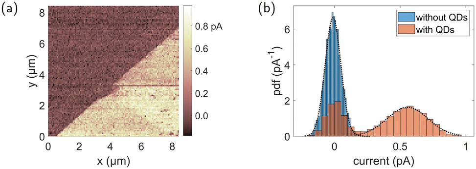 | ||
| Fig. 3 Peak force tapping pcAFM measurements on QD monolayer on ITO/glass. (a) Current map for a bias of 500 mV and an irradiance of 50 W cm−2 (delivered through the 10× objective) along an edge of the QD layer. (b) Histogram (bars) of the measured current values on the QDs (red) and on ITO (blue), scaled as probability density function (pdf). The black dotted lines show normal distributions with μ = −0.01 pA and σ = 0.06 pA and μ = 0.56 pA and σ = 0.16 pA. | ||
In Fig. 4(a) we summarize pcAFM scans of a 10 × 10 μm2 area with systematic variations of light irradiance (0–305 W cm−2, columns) and bias voltage (0–0.5 V, rows). The scan area has again been chosen around an edge of the QD layer (QDs removed in the upper left), to provide a background reference of the bare substrate. The irradiance and bias dependencies of the photocurrent are visualized in the heat map in Fig. 4(b), where the color-encoded currents correspond to the values averaged over the QD-covered areas in Fig. 4(a).
 | ||
| Fig. 4 Peak force tapping pcAFM measurements on a PbS/MAPbI3 QD monolayer on ITO. (a) Current maps for bias values of 0–500 mV (rows) and irradiances of 0–305 W cm−2 (columns), delivered through the 10× objective. The scan areas measure 10 × 10 μm2. (b) Heat map of the averaged current values over the QD-covered areas of panel (a). (c) Measured irradiance-dependent currents (symbols) and power law fits (lines) for each bias voltage. (d) Fit of Ohm's law to the voltage-dependent current, scaled by the derived power law with α = 0.64, P* = P/(1 W cm−2), P being the corresponding irradiance. | ||
From this data, we plot the irradiance dependence of the photocurrent for each applied bias voltage individually in Fig. 4(c). All dependencies follow a power law of the form I ∝ Pα, with a mean value for the bias-independent exponent of α = 0.64 ± 0.03. This value agrees very well with the range of α = 0.60–0.69 reported for PbS/MAPbI3 QDs on glass measured in a flat gold electrode arrangement.20Fig. 4(d) shows the associated I/V curve for the photocurrent scaled by the deduced power law. The derived ohmic contribution of 0.5 pA V−1 for an applied light irradiance of 25 W cm−2 corresponds to a resistance of 2 TΩ. This leads to a specific contact resistance of about 0.5 Ω cm2 for an assumed contact area of 25 nm2, corresponding to a parallel contact of about three QDs. We note that while in further experiments we have significantly increased the applied irradiances above the values reported in Fig. 4(c), signs of sample deterioration around 1000 W cm−2 prompted us to restrict our analysis to values well below this value.
For comparison, we have investigated a similar sample that is built from three layers of PbS/SCN QDs. Again, we achieved stable and reproducible imaging conditions when varying light irradiance and bias voltage, as summarized in the ESI, S4.† With the SCN ligands, the photoresponse of the PbS QDs is markedly different as compared to the perovskite shell, showing an irradiance power law exponent of 0.35 ± 0.03. As this value is well below the minimum value of 0.5 for pure photoconductance, effects as photogating34,35 are likely involved. Furthermore, the zero-bias current has opposite sign as compared with the PbS/MAPbI3 QDs. It has already been shown that the choice of ligands has a significant influence on the QD energy levels and a shift of up to 0.9 eV has been observed for PbS QDs.36 In this context, it might also be of interest that the surface charge in solution is negative for the perovskite-capped QDs13 and positive for the SCN-capped QDs.37
We now turn to the role of the substrate and add gold micro- and nanostructures to the ITO/glass substrate. This is motivated by the use of structured gold films as electrodes for QD optoelectronics20 and the potential role of an plasmonic field enhancement to modify the QD charge dynamics.38,39 Evidently, nanostructures in general and highly confined fields in particular call for a high-resolution method as scanning probe microscopy.
We thus explore the imaging capabilities of pcAFM on structured gold thin films covered with a monolayer of PbS/MAPbI3 QDs. Reference measurements on bare gold structures show that no stable and reproducible imaging conditions with PtIr tips can be achieved, as observed for gold surfaces before.40 Rather, sporadic contact was established around roughness features or particle edges, where interaction forces are expected to be high due to the finite response time of the feedback controlling the tip position (see the ESI, S5†). In contrast, QD-covered gold structures provide continuous contact and correspondingly stable and reproducible scan conditions. Fig. 5(a) and (b) show the topography and the current map, respectively, of a curved gold stripe 1 μm wide. The illuminating laser was focused by the 10× objective to a center irradiance of 400 W cm−2 and a bias voltage of 100 mV was applied. In this case the gold film blocks most of the exciting light and the QDs in the shadowed region show practically zero photoconductance, as opposed to the few-pA photocurrent from the illuminated QDs on ITO.
 | ||
| Fig. 5 pcAFM imaging of gold structures covered with a QD monolayer for a laser irradiance of 400 W cm−2 delivered through the 10× objective and 100 mV bias voltage. Contact AFM mode with 0.6 nN setpoint force was used. (a) Topography of a 1 μm wide curved gold stripe, (b) corresponding current map. (c) Topography of a dimer of nanotriangles with a side length of about 100 nm, (d) corresponding current map; the inset depicts the current map before adding the QD monolayer, evidencing the different conductivities of the two particles. | ||
In contrast, Fig. 5(c) and (d) depict two adjacent gold nanotriangles covered by the QD monolayer. Here, the gold structures are significantly smaller than the laser wavelength and their enhanced optical near field is expected to drive increased photocurrents, as compared to the bare ITO surface. This is indeed observed for the nanoparticle on the right side in Fig. 5(d). However, less photocurrent is measured on the left-side particle, an effect found for the majority of the nanotriangle dimers investigated. As evidenced by the current map of the particle pair before QD deposition (inset of Fig. 5(d)), this is a property of the particles and not a feature induced by the QD layer. At this point, we can only speculate about the underlying reasons, that are most likely related to a contact issue between the ITO substrate and the gold. We chose nevertheless to discuss this point here, as it nicely demonstrates the need for a high-resolution technique to identify local conductance when it comes to the characterization of nanostructures.
We finally ask for the light irradiance dependence of the photocurrent for the PbS/MAPbI3 QD monolayer on the gold nanotriangles. In Fig. 6, we plot the data as retrieved from a series of current maps on and next to the nanoparticles in Fig. 5(c) and (d). On the neighboring bare ITO substrate, an exponent of 0.64 ± 0.05 is found, corresponding to the value measured before (compare Fig. 4). However, a value of 0.93 ± 0.03 is retrieved from the gold nanotriangles, identical for both (presumably differently conducting) particles. We conclude that the charge dynamics of the QD monolayer is strongly determined by the supporting electrode material. While the exploration of the underlying mechanisms is beyond the scope of this study, we can speculate that modifications of the gold particles due to absorption and/or of the QDs in contact with gold occur. While this effect is quite pronounced for switching from ITO to gold, we note that the same power law exponent is found for ITO and glass, the latter being deduced from SPCM measurements.20
 | ||
| Fig. 6 Measured irradiance-dependent currents (symbols) and power law fits (lines) for a QD monolayer on two different gold nanotriangles (black, magenta) and on ITO (blue). Contact mode with 0.6 nN setpoint force, 0.1 V bias voltage and focusing by the 10× objective. | ||
Conclusion
In summary, we have applied pcAFM to quantitatively characterize the photoconduction properties of PbS/MAPbI3 QDs, deducing with high precision quantitative values for barrier height, built-in voltage, diffusion constant and ideality factor. The photocurrent was shown to dominate for biases below ±1 V. With respect to the dependence of the photocurrent on the light irradiance, a power law with an exponent of 0.64 was found, identical to the value reported for SPCM on planar electrode geometries.We hint at a wider applicability of pcAFM for quantitatively probing QDs by complementary measurements of PbS QDs with SCN ligands and underlying gold micro- and nanostructures. Meeting the need for ever smaller detection areas, the high spatial resolution of a photocurrent-detecting scanning probe will be a strong player in the characterization of single QDs41 and in complementing static hybrid QD/nanoparticle measurements.39
Experimental methods
PbS/MAPbI3 QD synthesis
The synthesis of PbS/MAPbI3 QD inks has been performed as described before.20 First, hydrophobic PbS QDs capped with lead oleate were synthesized following Hines et al.42 For that, Pb(CH3COO)2·3H2O (1.5 g, 4 mmol), ODE (47.5 mL) and oleic acid (2.5 mL, 7.07 mmol) were mixed in a three-neck flask. The mixture was degassed under a vacuum at 120 °C for 1 hour and cooled down to 90 °C under nitrogen flow. The heating mantle was removed and a solution of bis(trimethylsilyl)sulfide (TMS2S, 0.42 mL, 2 mmol) in 10 mL of dried ODE was injected into the vigorously stirred lead oleate solution at 85 °C. After 1 min, 3 mL of dried oleic acid were injected and the reaction mixture was cooled down to room temperature with an ice bath. The NCs were washed three times with hexane/ethanol solvent/nonsolvent pairs (30/144, 30/36 and 15/7 mL of hexane/ethanol at each step, respectively) and redissolved in 8 mL hexane. The washing cycles were performed in air, but the final pellet after the third cycle was redissolved in anhydrous hexane, filtered through a 0.2 μm PTFE filter, and stored in a glovebox. Second, a solution-phase ligand exchange was carried out. Typically, 10 mL of a 50 mM MAPbI3 solution in N-methylformamide was combined with 10 mL of oleate-capped PbS CQDs in hexane at a concentration of 5 mg mL−1. The mixture was stirred with a magnetic stirrer until all the CQDs were transferred into the polar phase (12 hours). The top phase was then discarded, and the bottom phase was washed three times with hexane. The ligand-exchanged CQDs were subsequently precipitated by adding an equal volume of acetone and collected by centrifugation. The supernatant was discarded, and the pellet was redispersed in 2.5 mL of 2,6-difluoropyridine at a concentration of 20 mg mL−1.PbS/SCN QD film preparation
30 μL of a solution with 10 g L−1 of oleic-acid-capped PbS QDs (Sigma-Aldrich product number: 900733) in toluene was first spin coated at 3000 rpm. The native ligands were then exchanged by subsequent spin coating 30 μL of 10 g L−1 NH4SCN in acetone at 3000 rpm and rinsing with acetone at 3000 rpm, following a modified process as described by Fafarman et al.37Author contributions
Florian Küstner did all experimental work, data analysis and modelling and wrote the initial draft. Harald Ditlbacher provided support on the experimental setup and contributed to the data analysis. Andreas Hohenau contributed to the data analysis and the modelling. Dmitry N. Dirin and Maksym Kovalenko provided the PbS/MAPbI3 QDs and supported sample fabrication. Joachim R. Krenn conceptualized and supervised the work and edited the final draft. All authors read and revisioned the manuscript.Data availability
All analyzed and discussed data are shown in the article or the ESI.† In particular, we refer to the tabular character of Fig. 4 and Fig. S3,† containing 35 and 18 individual photocurrent maps, respectively.Conflicts of interest
There are no conflicts to declare.Acknowledgements
The authors acknowledge the financial support by the University of Graz.References
- Z. Mamiyev and N. O. Balayeva, Mater. Today Sustain., 2023, 21, 100305 Search PubMed.
- G. Konstantatos, I. Howard, A. Fischer, S. Hoogland, J. Clifford, E. Klem, L. Levina and E. H. Sargent, Nature, 2006, 442, 180–183 CrossRef CAS PubMed.
- R. Saran and R. J. Curry, Nat. Photonics, 2016, 10, 81–92 CrossRef CAS.
- K. Xu, W. Zhou and Z. Ning, Small, 2020, 16, 2003397 CrossRef CAS PubMed.
- Z. Wu, Y. Ou, M. Cai, Y. Wang, R. Tang and Y. Xia, Adv. Opt. Mater., 2023, 11, 2201577 CrossRef CAS.
- M. Yuan, M. Liu and E. H. Sargent, Nat. Energy, 2016, 1, 16016 CrossRef CAS.
- M. V. Kovalenko, M. Scheele and D. V. Talapin, Science, 2009, 324, 1417–1420 CrossRef CAS PubMed.
- A. Dong, X. Ye, J. Chen, Y. Kang, T. Gordon, J. M. Kikkawa and C. B. Murray, J. Am. Chem. Soc., 2011, 133, 998–1006 CrossRef CAS PubMed.
- J.-S. Lee, M. V. Kovalenko, J. Huang, D. S. Chung and D. V. Talapin, Nat. Nanotechnol., 2011, 6, 348–352 CrossRef CAS PubMed.
- S. J. Oh, N. E. Berry, J.-H. Choi, E. A. Gaulding, H. Lin, T. Paik, B. T. Diroll, S. Muramoto, C. B. Murray and C. R. Kagan, Nano Lett., 2014, 14, 1559–1566 CrossRef CAS PubMed.
- O. Voznyy, B. R. Sutherland, A. H. Ip, D. Zhitomirsky and E. H. Sargent, Nat. Rev. Mater., 2017, 2, 17026 CrossRef CAS.
- W. Wang, M. Zhang, Z. Pan, G. M. Biesold, S. Liang, H. Rao, Z. Lin and X. Zhong, Chem. Rev., 2022, 122, 4091–4162 CrossRef CAS PubMed.
- D. N. Dirin, S. Dreyfuss, M. I. Bodnarchuk, G. Nedelcu, P. Papagiorgis, G. Itskos and M. V. Kovalenko, J. Am. Chem. Soc., 2014, 136, 6550–6553 CrossRef CAS PubMed.
- Z. Ning, O. Voznyy, J. Pan, S. Hoogland, V. Adinolfi, J. Xu, M. Li, A. R. Kirmani, J.-P. Sun, J. Minor, K. W. Kemp, H. Dong, L. Rollny, A. Labelle, G. Carey, B. Sutherland, I. G. Hill, A. Amassian, H. Liu, J. Tang, O. M. Bakr and E. H. Sargent, Nat. Mater., 2014, 13, 822–828 CrossRef CAS PubMed.
- H. Zhang, J. Jang, W. Liu and D. V. Talapin, ACS Nano, 2014, 8, 7359–7369 CrossRef CAS PubMed.
- D. Bederak, N. Sukharevska, S. Kahmann, M. Abdu-Aguye, H. Duim, D. N. Dirin, M. V. Kovalenko, G. Portale and M. A. Loi, ACS Appl. Mater. Interfaces, 2020, 12, 52959–52966 CrossRef CAS PubMed.
- N. Sukharevska, D. Bederak, V. M. Goossens, J. Momand, H. Duim, D. N. Dirin, M. V. Kovalenko, B. J. Kooi and M. A. Loi, ACS Appl. Mater. Interfaces, 2021, 13, 5195–5207 CrossRef CAS PubMed.
- S. Kudera, Y. Zhang, E. Di Fabrizio, L. Manna and R. Krahne, Phys. Rev. B: Condens. Matter Mater. Phys., 2012, 86, 075307 CrossRef.
- D. B. Strasfeld, A. Dorn, D. D. Wanger and M. G. Bawendi, Nano Lett., 2012, 12, 569–575 CrossRef CAS PubMed.
- D. Grimaldi, E. Kelderer, D. N. Dirin, M. V. Kovalenko, A. Hohenau, H. Ditlbacher and J. R. Krenn, Nanoscale Adv., 2022, 4, 3566–3572 RSC.
- Conductive atomic force microscopy, ed. M. Lanza, Wiley-VCH, Weinheim, 1st edn, 2017 Search PubMed.
- R. Giridharagopal, P. A. Cox and D. S. Ginger, Acc. Chem. Res., 2016, 49, 1769–1776 CrossRef CAS PubMed.
- H. Si, S. Zhang, S. Ma, Z. Xiong, A. Kausar, Q. Liao, Z. Zhang, A. Sattar, Z. Kang and Y. Zhang, Adv. Energy Mater., 2020, 10, 1903922 CrossRef CAS.
- D. C. Coffey, O. G. Reid, D. B. Rodovsky, G. P. Bartholomew and D. S. Ginger, Nano Lett., 2007, 7, 738–744 CrossRef CAS PubMed.
- M. Y. Teferi, H. Malissa, A. B. Morales-Vilches, C. T. Trinh, L. Korte, B. Stannowski, C. C. Williams, C. Boehme and K. Lips, ACS Appl. Nano Mater., 2021, 4, 2404–2412 CrossRef CAS.
- Y. Shao, Y. Fang, T. Li, Q. Wang, Q. Dong, Y. Deng, Y. Yuan, H. Wei, M. Wang, A. Gruverman, J. Shielda and J. Huang, Energy Environ. Sci., 2016, 9, 1752–1759 RSC.
- G. E. Eperon, D. Moerman and D. S. Ginger, ACS Nano, 2016, 10, 10258–10266 CrossRef CAS PubMed.
- K. Xu, W. Sun, Y. Shao, F. Wei, X. Zhang, W. Wang and P. Li, Nanotechnol. Rev., 2018, 7, 605–621 CrossRef CAS.
- A. Rose, Concepts in photoconductivity and allied problems, Interscience Publishers, New York, 1963 Search PubMed.
- E. Rhoderick and R. Williams, Metal-Semiconductor Contacts, Oxford University Press, Oxford, 2nd edn, 1988 Search PubMed.
- S. Arya, Y. Jiang, B. Jung, Y. Tang, T.-N. Ng, S. Oh, K. Nomura and Y.-H. Lo, Nano Lett., 2023, 23, 9943–9952 CrossRef CAS PubMed.
- S. Nehate, A. Prakash, P. D. Mani and K. Sundaram, ECS J. Solid State Sci. Technol., 2018, 7, P87–P90 CrossRef CAS.
- H. Kawano, Prog. Surf. Sci., 2008, 83, 1–165 CrossRef CAS.
- M. Buscema, J. O. Island, D. J. Groenendijk, S. I. Blanter, G. A. Steele, H. S. J. van der Zant and A. Castellanos-Gomez, Chem. Soc. Rev., 2015, 44, 3691–3718 RSC.
- H. Fang and W. Hu, Adv. Sci., 2017, 4, 1700323 CrossRef PubMed.
- P. Brown, D. Kim, R. Lunt, N. Zhao, M. Bawendi, J. Grossman and V. Bulovic, ACS Nano, 2014, 8, 5863–5872 CrossRef CAS PubMed.
- A. Fafarman, W. Koh, B. Diroll, D. Kim, D.-K. Ko, S. Oh, X. Ye, V. Doan-Nguyen, M. Crump, D. Reifsnyder, C. Murray and C. Kagan, J. Am. Chem. Soc., 2011, 133, 15753–15761 CrossRef CAS PubMed.
- O. Bitton, S. N. Gupta and G. Haran, Nanophotonics, 2019, 8, 559–575 CrossRef CAS.
- J. Huang, S. Hu, D. Kos, Y. Xiong, L. A. Jakob, A. Sanchez-Iglesias, C. Guo, L. M. Liz-Marzan and J. J. Baumberg, ACS Nano, 2024, 18, 3323–3330 CrossRef CAS PubMed.
- D.-Z. Guo, S.-M. Hou, G.-M. Zhang and Z.-Q. Xue, Appl. Surf. Sci., 2006, 252, 5149–5157 CrossRef CAS.
- K. Maturova, S. U. Nanayakkara, J. M. Luther and J. van de Lagemaat, Nano Lett., 2013, 13, 2338–2345 CrossRef CAS PubMed.
- M. Hines and G. Scholes, Adv. Mater., 2003, 15, 1844–1849 CrossRef CAS.
Footnote |
| † Electronic supplementary information (ESI) available: Estimation of the local irradiance, estimation of the number of contacted QDs, I/V model, pcAFM on PbS QDs ligand-exchanged with SCN, cAFM on gold structures. See DOI: https://doi.org/10.1039/d4nr02575j |
| This journal is © The Royal Society of Chemistry 2024 |