
 Open Access Article
 This Open Access Article is licensed under a
 Creative Commons Attribution 3.0 Unported Licence
Exciton diffusion in organic semiconductors: precision and pitfalls
Drew B.
Riley
 ,
Paul
Meredith
and
Ardalan
Armin
,
Paul
Meredith
and
Ardalan
Armin
Sustainable Advanced Materials (Sêr-SAM), Centre for Integrative Semiconductor Materials (CISM), Department of Physics, Swansea University Bay Campus, Swansea SA1 8EN, UK. E-mail: d.b.riley@swansea.ac.uk; paul.meredith@swansea.ac.uk; ardalan.armin@swansea.ac.uk
First published on 13th August 2024
Abstract
Nanometer exciton diffusion is a fundamental process important in virtually all applications of organic semiconductors. Many measurement techniques have been developed to measure exciton diffusion length (LD) at the nanometer scale; however, these techniques have common challenges that the community has worked for decades to overcome. In this perspective, we lay out the principal challenges researchers need to overcome to obtain an accurate measurement of LD. We then examine the most common techniques used to measure LD with respect to these challenges and describe solutions developed to overcome them. This analysis leads to the suggestion that static quenching techniques underestimate LD due to uncertainties in the quenching behavior, while time-resolved exciton–exciton annihilation (EEA) techniques overestimate LD based on experimental conditions, we advance steady-state EEA techniques as an alternative that overcome many of the challenges of these other techniques while preserving accuracy. We support this hypothesis with a meta-analysis of LD measured across various organic semiconductors and measurement techniques. We intend this investigation to provide a framework for researchers to interpret and compare findings across measurement techniques and to guide researchers on how to obtain the most accurate results for each technique in question.
 Drew B. Riley | Drew Riley received his PhD from Swansea University in 2023, he is currently a Post Doctorial Research Assistant at the Centre for Integrative Semiconductor Materials. His research interests include fundamental light matter interaction as well as charge and exciton transport in disordered semiconductors within optoelectronic applications such as photodetection and solar energy conversion. |
 Paul Meredith | Paul Meredith is Professor of Materials Physics at Swansea University and Director of the Centre for Integrative Semiconductor Materials. He is also an Honorary Professor at the University of Queensland and obtained his PhD from Heriot Watt University in Edinburgh. Paul's research interests lie in sustainable advanced materials including molecular semiconductors for applications in bioelectronics, solar energy conversion and optoelectronics. |
 Ardalan Armin | Ardalan Armin obtained his Ph.D. in Physics from the University of Queensland, Australia in 2014 and joined Swansea University in 2017. His current research and teaching activities focus on next generation materials for optoelectronics, semiconductor device physics, and micromechanical systems for sensing. He is currently an Honorary Associate Professor of Physics at Swansea University and a Senior Technologist at Collins Aerospace. |
1 Introduction
The transport of quasiparticles in semiconducting crystals, or any other semiconducting media, lies on a spectrum which is typically characterized by the extrema shown in Fig. 1. On the right end lies band transport where the wavefunction of the quasiparticle expands indefinitely in 3 dimensions across the media, leading to efficient band-transport. On the left end of the spectrum the wavefunction of the quasiparticle is confined to one atom (or a collection of nearby atoms), leading to inefficient defect-hopping transport. The confinement of the wavefunction is not controlled solely by the atomic composition of the media as the local environment, such as the ionicity of crystal bonding, or the larger crystal structure, such as the dimensionality, the dielectric environment, the crystallographic strain, or the lattice temperature can alter the wavefunction confinement, and hence quasiparticle transport.1 Between these two extrema lies the intermediate regime where quasiparticle transport cannot be fully described by either defect hopping or band transport. Many modern materials fall into the intermediate regime such as conductive metal–oxide frameworks,2 hybrid organic–inorganic perovskites,3–5 quantum dots,6 2D materials,1 and disordered organic semiconductors.7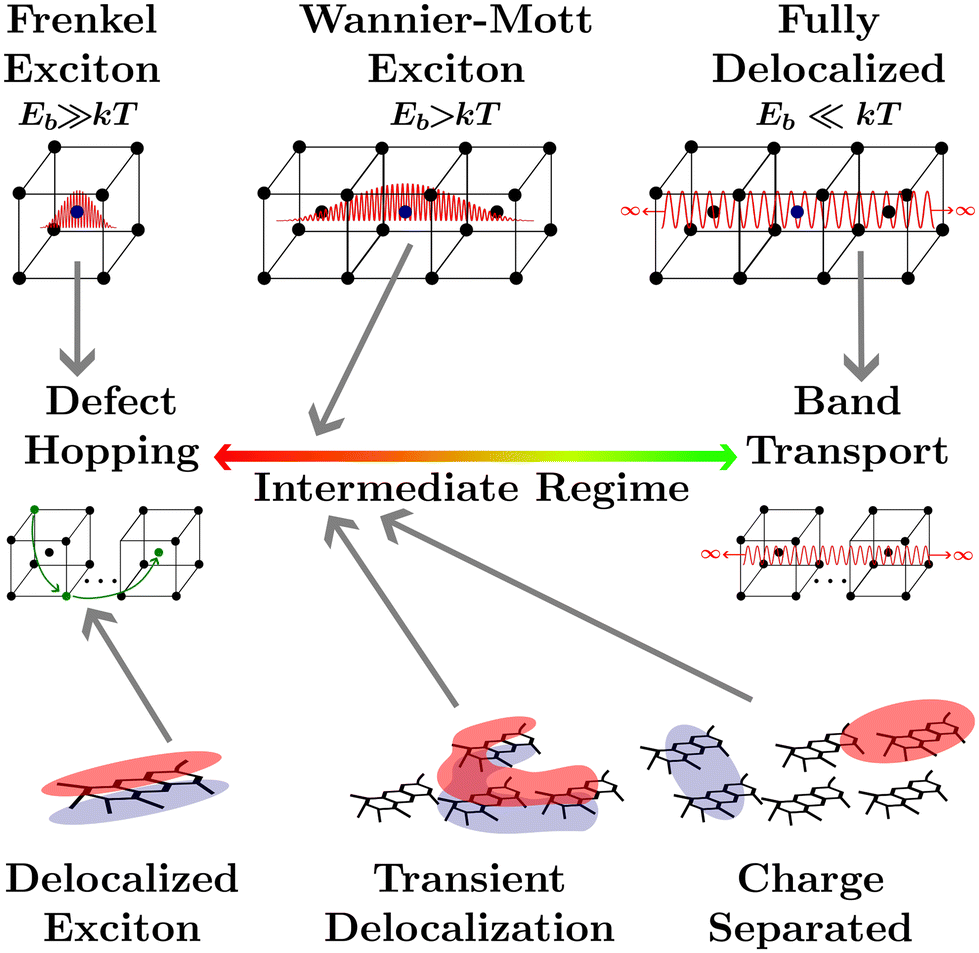 | ||
| Fig. 1 An illustration of the quasiparticle transport spectrum in solids. Top row-the difference between quasiparticle confinement in a body-centred cubic solid-state crystal. Middle row-the quasiparticle transport spectrum from inefficient defect hoping to efficient band transport. Bottom row-the excitonic structure of polymers and polymer films including excitons delocalized across a single polymer, transient delocalized excitons, and delocalized charge separated states. | ||
Upon light absorption by a semiconducting crystal, excitations localized to a single atom or a collection of nearby atoms known as excitons are formed which are characterized by a bound electron hole pair and an associated coulombic binding energy (Eb).1,8 Frenkel excitons are heavily localized to one or nearest neighbor atoms in a crystal and therefore are characterized by large Eb.8 The transport of Frenkel excitons in semiconductor crystals is described by an even distribution of low-density defect states with an electron affinity below the band edge of the insulator they are embedded in.8 This leads to what has become known as hopping transport between defect sites where the coupling is induced by the exciton wavefunction extending into the insulating material.8,9 With a slightly smaller Eb, Wannier–Mott exciton wavefunctions extend to fill at least one unit cell.1 Often used to describe semiconducting crystals with small bandgaps or low-dimensional semiconductors, the extended wavefunctions will allow for more efficient transport, somewhere in the intermediate regime.1 If the kinetic energy of the electron and hole pair exceeds Eb, for example through decreasing the dielectric screening or increasing the lattice temperature, the electron and hole may dissociate to the point where the Coulomb force is insignificant. Under these conditions the electron and hole are considered to be in a charge-separated state where the binding energy is effectively negligible. Although the process of local excitation → exciton → charge separated state is universal to all semiconducting media, in many materials these processes are fleetingly fast and are therefore disregarded. The characterization of a media as excitonic or not depends on how delocalized the excitonic wavefunction is and therefore where on the quasiparticle transport spectrum the media lies. However, it is important to note that the excitonic status of any media depends on extraneous factors such as lattice temperature, strain, or dimensionality.1
The focus of this perspective will be on the excitonic transport properties of one class of semiconducting media that is typically understood as excitonic, organic semiconductors, and their application to organic photovoltaics (OPVs), encompassing photodiodes and solar cells. The planar structure common to these conjugated polymers leads to three covalent sp2 hybridized orbitals between carbon atoms while the remaining unhybridized orbital creates a π-system adjacent to the molecular plane.7 This arrangement leads to rigid molecular backbones which contribute to partially delocalized excitonic states across a polymer, as shown in the lower left of Fig. 1, and high oscillator strengths.10,11 The optical gap (Eopt) associated with these oscillators is often taken to be the difference between the highest occupied molecular orbital (HOMO) and lowest unoccupied molecular orbital (LUMO) levels of the polymer in the ground state.10 Although it is important to note that the HOMO and LUMO levels are merely convenient constructs analogous to the frontier orbitals that make up band edges in periodic semiconductors. Additionally, accurately measuring the HOMO and LUMO levels in organic semiconductors comes with many challenges.12
Deposition of solid-state films through solution processing or thermal evaporation of these high oscillator strength polymers results in films with high absorption coefficients but large amounts of energetic disorder.13 Coupled with weak van der Waals bonding between molecules the high energetic disorder limits the extent to which excitonic states delocalize across neighboring molecules. Concurrently, low dielectric constants lead to limited dielectric screening, further constricting wavefunction delocalization.14,15 Hence, each individual polymer is often understood as a single lattice point in solid-state film made from organic semiconductors. For this reason an analogy is often brought between excitations in organic semiconductors and Frenkel excitons, placing organic semiconductors at the defect hopping extrema of the quasiparticle transport spectrum.
However, calculating exciton transport under these assumptions from first principles has been vexing for researchers as transport measurements have often exceeded the expected result by orders of magnitude.16,17 The assumption of a defect hopping level associated with Frenkel excitons is clearly inapplicable to organic semiconductors as it is the lack of dielectric screening and the disorder of the conjugated polymers that confine the wavefunction, rather than any embedded energetic offset. How organic semiconductors can exhibit high excitonic transport properties with low electrostatic screening and high energetic disorder is still an open question.
One recently proposed solution to this question comes about by partially relaxing the assumption that excitonic wavefunctions are localized to a single polymer. Researchers allow for the excitons to form partially delocalized states which can take on irregular shapes and extend over more than one molecule. This has been computationally explored to investigate how partially delocalized excitons diffuse using fully atomistic, quantum-mechanical, surface hopping, and delocalized kinetic Monte-Carlo (kMC) approaches.18–23 This research has indicated that small regions of large delocalization in organic semiconducting films, known as transient delocalization, significantly increases both the excitonic and charge transport properties. Despite the lack of a rigid crystal lattice to allow for a clear definition of unit cells or Wannier–Mott excitons this analogous delocalization is sufficient to shift the transport properties of organic semiconductors into the intermediate regime of the quasiparticle transport spectrum, where defect hopping transport can no longer fully describe transport phenomena.18,20,23
The transport of excitons in organic semiconductors is uniquely important to OPVs, as the generation of useful current is dependent on splitting the tightly bound excitons.7,24 This is commonly achieved by creating a heterojunction of two organic semiconductors known as the acceptor (higher electron affinity) and the donor (lower electron affinity). An exciton near the heterojunction interface in the donor (acceptor) phase may transfer the electron (hole) to the acceptor (donor) phase forming what is commonly known as a charge transfer (CT) state.25 The donor and acceptor molecules are chosen such that the energetic difference at the interface decreases the enthalpy for the charge separation reaction.10 This enables exciton separation at operational temperatures assisted by the entropic driving forces within each side of the heterojunction.26–28 Common examples of heterojunctions include bulk heterojunction (BHJ),25 bilayers,29 pseudo-bilayers,30,31 and dispersed low-donor heterojunctions.32–34 However, as the excitation is confined to a single polymer in either the donor or acceptor phase, prior to the splitting of charges the exciton must be transported to the heterojunction interface either through diffusion in the excited phase or Förster resonance energy transfer (FRET) to the opposing phase followed by diffusion to the interface.35,36 The diffusion followed by charge transfer process is illustrated in Fig. 2. In this illustration the exciton (Ex) is optically generated inside the donor phase of a bulk heterojunction. The exciton then diffuses to the interface between the donor and acceptor phase where, due to the differences in electron affinity and electrostatic interactions at the interface,7,26 electron transfer occurs from the donor to acceptor resulting in a bound CT-state with the electron in the acceptor phase and the hole in the donor phase. The choice of donor and acceptor material in any heterojunction is of upmost importance to ensure that both the nano-morphology of the heterojunction allows for efficient diffusion and the energetics of the CT-state allow for efficient separation of electrons and holes which can then be transported to the electrode and extracted as current. In many modern materials the offset between HOMO levels has been reduced allowing for an efficient back-electron transfer processes which reform singlet or triplet excitons from CT-states providing additional loss pathways in photovoltaic devices.7,37–39
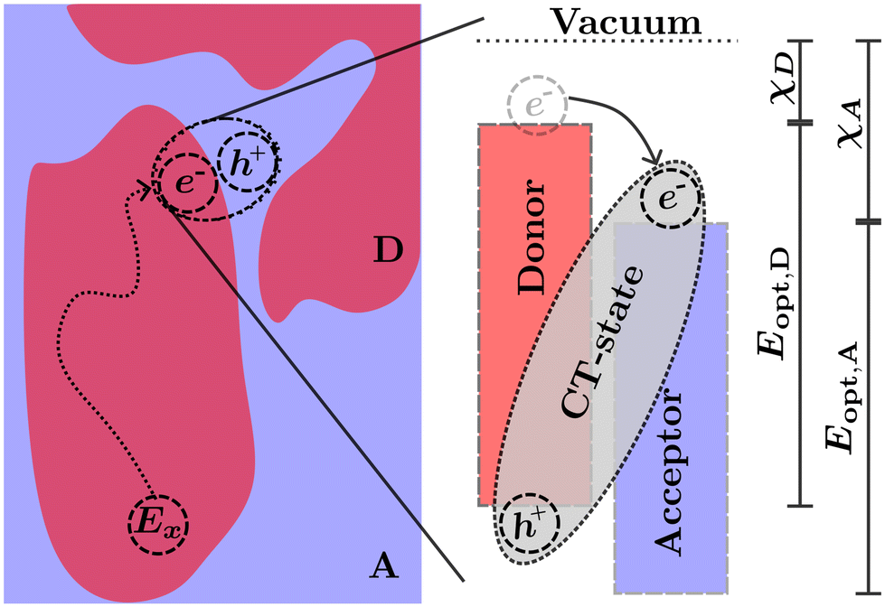 | ||
Fig. 2 The diffusion and charge transport process in photovoltaics based on organic solar cells. (Left) An exciton (Ex) is generated in the donor (D) phase of a bulk-heterojunction, Ex then diffuses to the donor acceptor (A) interface. Electron transfer of the electron from the donor to the acceptor occurs resulting in a CT-state. (Right) The energetics at the D![[thin space (1/6-em)]](https://www.rsc.org/images/entities/char_2009.gif) :A interface and the formation of a CT-state through electron transfer. χD-electron affinity of donor, χA-electron affinity of acceptor, Eopt,D optical gap of donor, and Eopt,A optical gap of acceptor while neglecting the exciton binding energy. :A interface and the formation of a CT-state through electron transfer. χD-electron affinity of donor, χA-electron affinity of acceptor, Eopt,D optical gap of donor, and Eopt,A optical gap of acceptor while neglecting the exciton binding energy. | ||
The 2000s saw significant research efforts focused on understanding and measuring exciton diffusion lengths (LD) in organic semiconductors when diffusive process restricted photocurrent generation as LD of commonly used organic semiconductors were <10 nm.40 Organic semiconductors with small LD limited the space of possible heterojunctions capable of generating usable current to the BHJ with small domain sizes.7 Accurate quantification of LD became less important and somehow a redundant task in the following decade, as (almost all) fullerenes derivatives and typical donors of the time exhibit LD < 10 nm demanding very finely controlled nanomorphology and large interfacial area for efficient exciton separation.40,41 However, recent advancements in polymer design,38,39,42–44 polydispersity,45 purity, and film deposition26,46,47 have resulted in the report of measurements of LD > 10 nm.29,42,48,49 These increased diffusion lengths have been showcased using these modern polymers and small molecules (especially in the so-called non-fullerene acceptors (NFAs)) in alternative heterojunctions such as bilayers and pseudo bilayers.29–31,50 The introduction of NFAs resulted in a step growth of power conversion efficiency in OPV-based solar cells and a broadening of OPV-based photodetectors detectivity into the near infrared.7,24,50 Given the complexity of the nano-morphology in all these heterojunctions, measuring exciton diffusion has become an important objective for the community again.49 Accurate quantification of LD is required to determine the current generation capability of an organic semiconductor in a particular heterojunction and to gain a fundamental understanding of the processes limiting charge generation in OPVs. Overestimations of LD may lead to incorrectly ignoring diffusion-related losses to charge generation, or to utilizing unsuitable materials in particular heterojunctions. Underestimations of LD may lead to diminishing the potential for a particular organic semiconductor in a particular heterojunction. Quantification of LD is also crucial for finding design rules for materials and structure–property relationships for process optimization. Additionally, OPVs suffer from stability issues which have hindered their commercialization after two decades of continuous development and efficiency enhancement. One of the instability problems is morphological, where pseudo-bilayers enabled by increases in LD may be a solution.31
There have been many experimental methodologies to quantify LD in organic semiconductors such as FRET analysis,42,44,51 volume34,41,45,51–57 and bilayer quenching,29,35,50,58–64 time-resolved exciton–exciton annihilation (EEA),42,47,48,50,51,53,54,57,60,61,65–76 and steady-state EEA48,67,36,77,68 These techniques have been core to the community's current understanding of exciton dynamics in disordered systems including, but not necessarily limited to, exciton diffusion. With new material classes emerging, such as NFAs, it is timely to review these methodologies and to identify their operational windows and limitations. Different techniques may yield different results in the same material systems,42,51,68,78 while evidence of fluence dependence of LD complicates time-resolved EEA measurements.48,68,74,75 Further, in recent years these techniques have been adopted by a larger contingent of OPV and organic semiconductor researchers in holistic studies of charge generation in various applications, making accurate measurements essential to subsequent interpretation of results.29,30,49,77
In this perspective we will review and detail various methods for measuring nanoscale exciton diffusion and discuss their limitations and potential biases. We evaluate each methodology with respect to common experimental challenges that can lead to over- or under-estimations of LD. We go through these challenges systematically for the most widespread techniques laying out common solutions used by the organic electronics community. This discussion leads to the inference that static quenching experiments are most likely to underestimate LD while time-resolved EEA methods are most likely to overestimate LD; a conjecture that we will show is reflected in the wider literature. Further, we explain the origins of these over- and under-estimations and make recommendations for researchers to follow to avoid these pitfalls. This understanding has wide implications throughout the organic electronics and OPV research communities as novel small-molecule design has led to increases in LD sparking intense activity in novel OPV design relying on efficient diffusion, as well as a renaissance in the interest of LD measurements.49 In addition, as these techniques become increasingly widespread and used as evidence in studies by a broad range of researchers, the soundness and limitations of each technique must be clear and transparent to the community. We intend for this perspective to be valuable not only to established researchers but also to newcomers to the field, providing a pedagogical approach to understanding these measurements and the underlying physics.
2 Theory of exciton diffusion
Strong dipole–dipole interactions brought on by the large oscillator strengths of organic semiconductors allow for energy transfer to occur between molecules. The assumption that the spectral lines of the emitting and absorbing dipoles are both sharp and in resonance would indicate that the projection of one dipole (μ(E,A)) onto the other, as illustrated in Fig. 3(a), is the primary indicator of energy transfer leading to a transfer rate constant of ħμE·μA/r3, where ħ is the reduced Planck constant and r is the distance between dipoles. This assumption has been repeatedly discredited, showing a r−6 dependence.80 However, the emission and absorption spectra of organic semiconductors have broad spectral shapes due to energic disorder and aggregation, among other effects,7 meaning that molecules need only be in resonance for a short period of time for energy transfer to occur. This indicates that the rate constant for energy transfer can be related to the transition dipole moments and the probability of resonance as80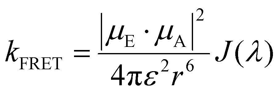 | (1) |
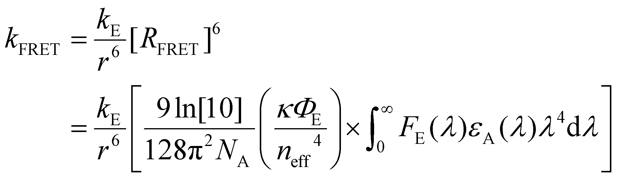 | (2) |
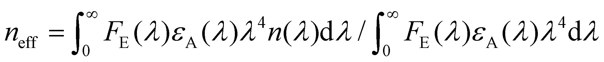 , n(λ) being the real part of the refractive index), all in the appropriate units.26
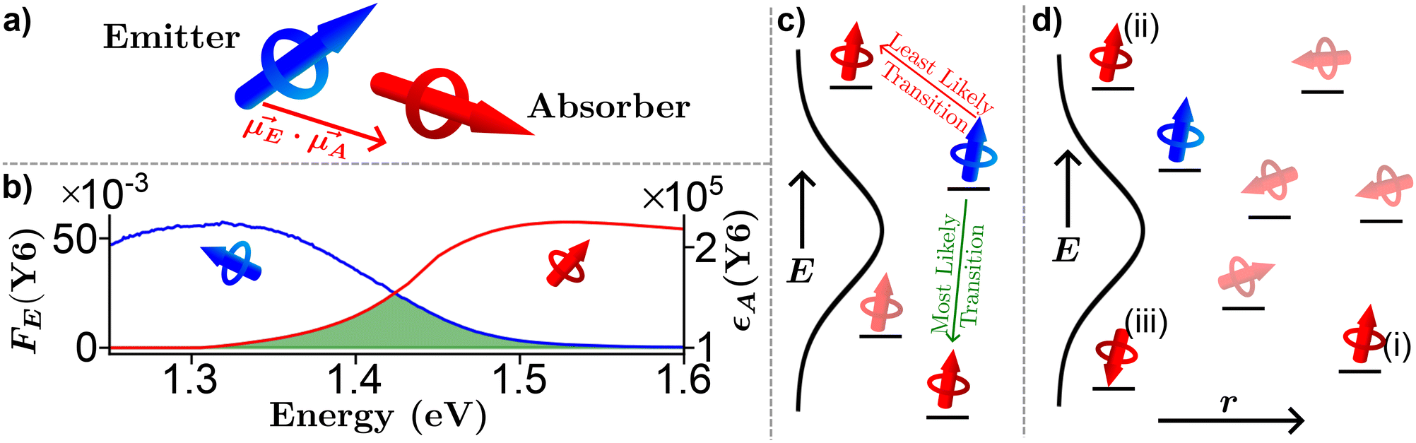 | ||
| Fig. 3 Pictorial representation of Förster resonance energy transfer (FRET) in organic semiconductors. (a) A lone emitter absorber pair. (b) Experimentally determined emitter fluorescence (FE, blue) and absorber extinction coefficient (εA, red) of Y679 thin film with the spectral overlap region outlined in green. (c) Energy dependence of FRET. (d) Combination of energy, orientation, and special dependence of FRET. | ||
The formalism laid out in eqn (2) provides some intuition as an increase in the spectral overlap region, the PLQY of the emitter, and the dipole orientation factor will increase both RFRET and kFRET through increased coupling between molecules, while a decrease in the refractive index will have the same effect through a reduction in the dielectric screening between emitter and absorber. For example, Fig. 3(b) shows the spectral features of FE(λ) and εA(λ) for a film made from the exemplary organic semiconductor Y679 (all chemical definitions are provided in the Notes and references section) with the overlap region highlighted in green. In the case of Y6, RFRET is calculated to be 1.7 nm, comparable to the intermolecular stacking in a film.17 This results in a high kFRET between neighboring molecules and hence hopping-like transport between molecules, i.e. exciton diffusion.
Up to now we have assumed that the only source of disorder is due to random orientation of dipoles. However, variations in molecular conformation, polydispersity, and chemical impurities result in a great deal of energetic disorder.13 This disorder is typically expressed as a Gaussian density of states (DOS) 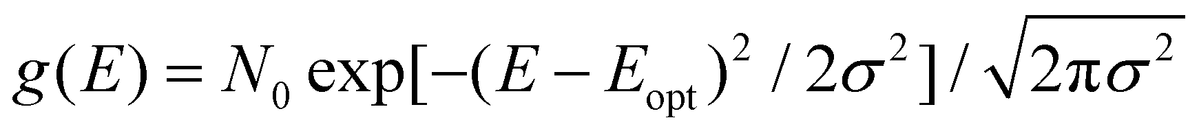 within the film, where E is the energy of a state, N0 is the number density of excitonic states, and σ quantifies the amount of disorder in eV. This DOS suggests that the diffusion process is governed by thermally activated hoping in a Gaussian energetic landscape in which excitons thermalize quickly downhill towards an equilibrium energy.40 This is shown graphically in Fig. 3(c) in which the emitter (shown in blue) should migrate lower in energy over time and the probability of migration should be given by the change in energy between the emitter (E) and absorber (A) site ΔE(E → A) = EA − EE. As excitons are charge-neutral with low reorganization energies exciton migration is typically viewed as a Miller–Abrahams type hopping process (see eqn (3)) in which the uphill jumps are modified by a Boltzmann factor to account for detailed balance.16,18 The Marcus model has also been used to account for possible reorganization energy associated with the electrostatic interaction of the exciton and the surrounding media.81 Nonetheless, Miller–Abraham is computationally light and due to low reorganization energy, seems to be a suitable assumption for exciton transport.
In addition to the random orientation of dipoles and the disordered energetic landscape, when deposited into semiconducting films organic semiconducting molecules are not arranged in a periodic structure. Therefore, the distances between neighboring molecules may vary throughout the film as shown projected onto one dimension in Fig. 3(d). Additionally, FRET allows for energy transfer between non-nearest neighbor pairs. To account for the variation in distance a phenomenological tunnelling factor is typically employed, defined by the inverse localization radius (ζ). This tunnelling was originally developed to explain impurity conduction in which wavefunctions exponentially decay into the surrounding media which, as mentioned above, is not the case for densely packed organic semiconducting films,8,9,22 we will return to this point in a subsequent paragraph.
Fig. 3(d) exemplifies the role of energetic and spatial disorder in exciton transport. The dipole of the emitter (shown in blue) is best aligned with the dipole of absorber (i) and (ii) and least aligned with absorber (iii) indicating that FRET should be least likely to (iii). However, absorber (ii) is an uphill jump the same distance as (iii) while (i) is a downhill jump at a longer distance. Accounting for each of these competing contributions to disorder the transfer rate constant between any two molecules in a film can be expressed as18,48
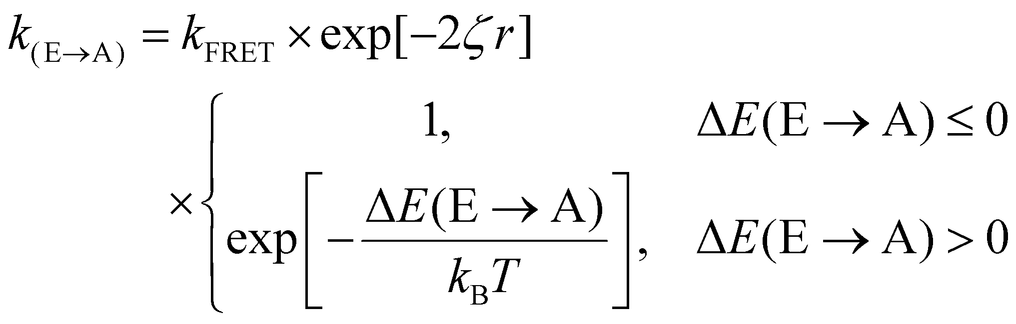 | (3) |
So far we have assumed that the exciton is confined to a single molecule in a film, when this assumption is relaxed transient delocalization can take effect and more complex models than eqn (3) are required to accurately reflect the underlying physics. However, under this relaxation the phenomenological tunnelling factor was rigorously justified in the context of polaron pairs near a heterojunction interface. By assuming that polarons form regular spherical shapes with a delocalization radius less than the intermolecular spacing the so-called distance-dependent delocalization correction can be simplified to the phenomenological correction where the tunnelling factor is a stand-in for the spatial extent of the delocalization.22 In principle this simplification can be applied to exciton transport as well since, due to the low reorganization energy, delocalization is assumed to occur over few molecules at most.18 Hence, the use of eqn (3) is sufficient as a computationally inexpensive stand-in for exciton transport in organic semiconducting films.
Utilizing eqn (3), the diffusion of excitons can be viewed as a random walk throughout a collection of molecules where the diffusion coefficient is given by the average distance of a jump (![[r with combining macron]](https://www.rsc.org/images/entities/i_char_0072_0304.gif) ) and the jumping frequency as D = k(E→A)/2d, where d is a unitless number related to dimensionality. LD can then be calculated knowing the average lifetime of a population of excitons (τ) as
) and the jumping frequency as D = k(E→A)/2d, where d is a unitless number related to dimensionality. LD can then be calculated knowing the average lifetime of a population of excitons (τ) as
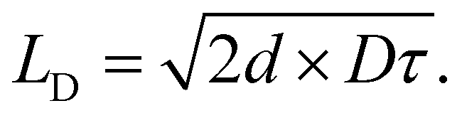 | (4) |
We note that often the factor of d or 2d is dropped for convenience; therefore, care must be taken when comparing results from different sources as contrasting definitions of LD can lead to extraneous factors up to  .
.
Fig. 4(a) illustrates various processes excitons can undergo in a neat organic semiconductor film or a heterojunction made with two organic semiconductors. The blue dipole indicates an exciton excited through absorption of a photon. Path (i) illustrates the diffusion process; the exciton proceeds to hop to between molecules along the red path labelled (i) until it recombines with rate constant kx = 1/τ. The distance traveled before recombination is then given as LD.
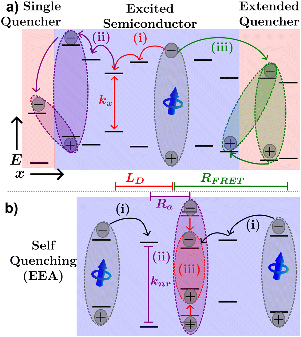 | ||
| Fig. 4 Excitonic processes in organic semiconductors. (a) Exciton created in the excited semiconductor can undergo diffusion until decay occurs (path i), electron transfer (path ii), or FRET transfer to a nearby quenching molecule, film, or phase (path iii), possibly followed by hole transfer. (b) Exciton–exciton annihilation processes, two excitons interact via FRET to produce a non-radiative decay and a thermalized exciton. | ||
Exciton quenching processes can occur in films containing two (or more) organic semiconductors either as a bilayer structure, a BHJ, or a small percentage of the host semiconductor. This process is illustrated in Fig. 4(a) path (ii). Instead of recombining within the excited organic semiconductor, the exciton diffuses to an interface between organic semiconductors as shown by the purple path (ii). If the quenching molecule LUMO (HOMO) level is lower (higher) than that of the excited organic semiconductor, electron (hole) transfer may occur resulting in a CT-state. Alternatively, FRET between organic semiconductors in a heterojunction may occur as described by eqn (2), where the emitter is the excited semiconductor, and the absorber is the unexcited semiconductor. FRET between semiconductors is depicted by the green path (iii) of Fig. 4(a). The energy transfer will most likely result in an exciton near the interface in the neighboring semiconductor or quenching molecule potentially forming a CT-state as described above. As CT-states PLQY are orders of magnitude lower than excitons these states will most likely decay non-radiatively, and the exciton is referred to as quenched.10
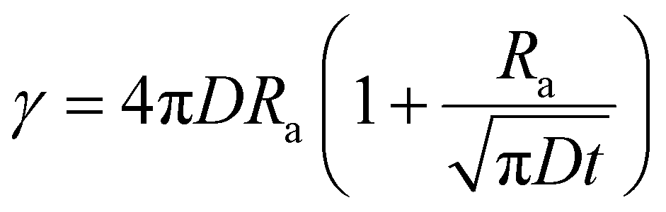
In cases of high excitation density excitons can undergo a self-quenching process known as exciton–exciton annihilation (EEA). Depicted in Fig. 4(b), two excitons diffuse towards one another, as shown in path (i), if they are within a critical radius, known as the annihilation radius (Ra), one exciton will decay non-radiatively while the other molecule will be briefly excited to a higher vibrational energy state in either the HOMO, LUMO, or both, illustrated by path (ii), before non-radiatively relaxing to the lowest excitonic state, as illustrated by path (iii). The rate equation for the density of excitons (ρ) in a film made from an organic semiconductor is given by
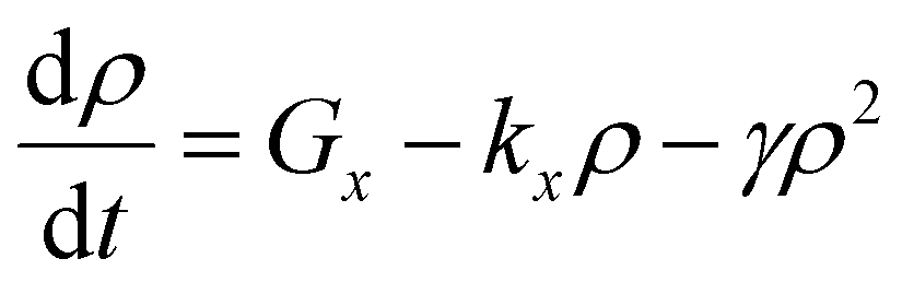 | (5) |
 | (6) |
3 Measuring exciton diffusion length
As stated in the introduction, there have been many creative ways to measure exciton diffusion in organic semiconductors.40 Rather than collate measurements on various material systems in this section we will endeavor to give an overview of the most common techniques focusing on the advantages, disadvantages, and inherent difficulties of each method and strategies researchers have developed to overcome them.We will focus our attention on fully optical techniques for measuring LD as these have emerged as favored methods due to the simplistic modelling required to extract diffusion characteristics. However, other techniques such as microwave conductivity, the external quantum efficiency (EQE) method, or surface photovoltage have historically been employed, while additional innovative techniques such as excitation correlation photoluminescence (ECPL) have been demonstrated on organic semiconductors.40,68,76,86–91
All optical measurements share some common challenges which will be outlined prior to the details of each technique. We will focus our attention on films made from P3HT-RR84 as there is a long history of measuring LD and D on P3HT-RR.40,48,61 However, the challenges, descriptions, and solutions described below apply to any disordered organic semiconductor film.
Challenge (i): low finesse optical cavity effects
High absorption coefficients and film thicknesses of order 100's of nm coupled with inevitable interfaces with the experimental atmosphere, substrate, or additional layers in a sample with refractive index differences cause complex optical field distributions within organic semiconductor films or devices.92,93 This is demonstrated in a transfer-matrix simulation in Fig. 5(a)–(c) where the absorption profile of a Y6 sample [Y6-PM683 bilayer] on glass exhibits complex spectral characteristics. Most optical techniques rely on some assumptions about the underlying absorption profile,63 how each technique deals with this challenge is detailed below. However, care must be taken to ensure that the assumed absorption profile is as precise as possible. Transfer-matrix models (TMM) combined with an accurate measure of optical constants are essential to validate these assumptions.93
 | ||
| Fig. 5 Optical absorption and decay characteristics of organic semiconductors. (a) Transfer matrix model of spectral and positional exciton generation rate in a Y6 film on glass structure. Red indicating high exciton generation, blue indicating low exciton generation. Transfer matrix model of positional exciton generation rate for a 100 nm (b) Y679 film on glass and (c) Y6:PM683 bilayer film on glass for an input wavelength of 800 nm (red), 515 nm (green), and 400 nm (blue). Time resolved photoluminescence with multiexponential fits (black) and linearized log–linear fits (green) for (d) P3HT-RR84 and (e) BTP-eC9.48,85 | ||
Challenge (ii): evaluation of low-density lifetime
The measurement of exciton lifetime, τ (or kx), required for converting between D and LD in eqn (4) and often required as an input to simulations or fitting algorithms, can be surprisingly difficult to quantify in organic semiconductor films. This is primarily due to EEA occurring over the course of a measurement, and in rare cases more exotic annihilation processes.32,33Fig. 5(d) shows a ‘low-density’ TRPL scan of a P3HT-RR84 thin film on a log–lin scale, where the effect of EEA can be seen at short time scales. To evaluate τ in the presence of these higher order effects the excitation density must be reduced. This can be accomplished by reducing the excitation power of the laser; however, this reduces the signal to noise ratio of the measurement. Alternatively, the thickness of the film can be increased; however, this leads to incorrect assumptions about the excitation profile and, hence, compounds challenge (i). To overcome this, researchers have developed a few strategies to evaluate τ using higher pump intensities. Multi-exponential fits are employed and an average of the fitting parameters29 or the longer of the two19,20 (or sometimes even three43) lifetimes is taken as a measure of τ. Other researchers use the time for the PL to fall to 1/e the original value as a proxy for the exciton lifetime in the low-density regime.57 However, as expressed in eqn (5) (solved for specific cases below in eqn (8)) these fittings do not reflect the underlying physics. In Fig. 5(d) the black dashed line indicates a multi-exponential fit where the two extracted lifetimes are 32 and 294 ps. Other researchers use the linear region of a log–lin plot and a linear fit to evaluate the longest lifetime.36,48 Although this approach is justified with respect to eqn (5) the choice of the range of the linear region is arbitrary and can affect extracted lifetime. In Fig. 5(d) the green dashed line represents a fit using this technique where the extracted lifetime is 335 ps. Others have chosen to use τ0 = 1/kE as a measure of the low-density lifetime, which in the case of P3HT-RR has been measured as high as 600 ps.94 However, the optical fluorescence properties have been shown to be very different between solutions and films making this assumption equally problematic.41 Another approach to minimize EEA is to use diluted films dispersed in a neutral solid-state host.42 Some concerns may be raised in this regard due to the question of morphological relevance of these systems to the semiconductor film in question and the similarity of excitation profiles with regards to challenge (i).
The primary recommendation to overcome this challenge is to utilize thin films (<50 nm) and low excitation powers such that the decay is described by a single exponential. In addition, the excitation wavelength can be tuned to a low absorption wavelength for the organic semiconductor in question.61 However, care must be taken as operating in the low-density regime may be below the detectivity of the experimental apparatus. Further, the low-density regime is system dependent and is determined ultimately by the diffusion length, as excitons that diffuse faster will inevitably interact more, while the ultimate detectivity will be determined by material-dependent factors such as the PLQY and spectral match between emission wavelength and detector responsivity. This system dependence is exemplified in Fig. 5(e) which shows photoluminescence decay for a BTP-eC985 thin film. In the case of BTP-eC9 the low-density lifetime is easier to measure, despite a LD about 3 times longer, and the decay appears much more single-exponential while the multi-exponential and log-space fits give similar results.48
Challenge (iii): quenching distances
The last three experimental techniques listed below can be grouped together as quenching experiments. In the optical version of these techniques the photoluminescence or transient absorption signal is observed under some varying parameter, such as quencher density, bilayer thickness, or exciton density. However, the distance over which the quenching processes occur is uncertain and this uncertainty will inevitably propagate to the quantified LD.34,57,63 As illustrated in Fig. 6, uncertainties can occur for (at least) three reasons. Fig. 6(a) illustrates what would be expected if quenching were a diffusion limited process in which the exciton hops directly onto the quenching molecule, in this case the geometrical distances between quenching molecules (black) and position the exciton is formed (blue) are indicative of how far an exciton could possibly diffuse as it typically assumed in any fitting model.63 However, it may be that the quencher acts as a well pulling excitons towards it by modulation of the electrostatics near the quencher interface as illustrated in Fig. 6(b).26 FRET between organic semiconductors and quenching molecules can occur on scales larger than the intermolecular spacing indicating that quenching can be a long-range process as illustrated in Fig. 6(c).63 In addition, as shown in Fig. 6(d), excitons are most likely delocalized across more than one molecule and the distances over which these interact with quenching centers or planes will be system dependent.17–20,23,34 As illustrated in Fig. 6 all these factors lead to measurements underestimating the diffusion length compared to the diffusion limited process. This analysis indicates that static quenching experiments are likely to underestimate LD in organic semiconductors, a conjecture that we will return to in sections 3.3 and 4.
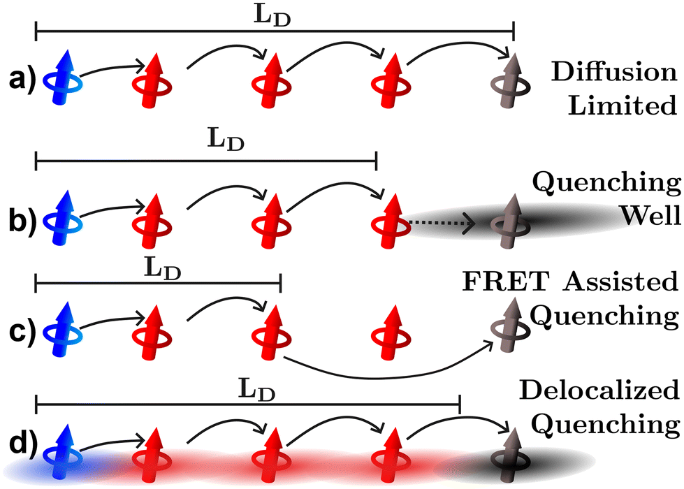 | ||
| Fig. 6 Pictorial representation of challenge (iii): quenching distances. Excitons generated on the blue dipole (polymer or molecule) diffuse through the red dipole and to the black quenching dipole. (a) The diffusion limited case as assumed by most quenching experiments. Underestimations can be caused by (b) quencher acting as a well pulling the excited exciton towards it, (c) FRET assisted quenching, or (d) delocalization assisted quenching. | ||
Challenge (iv): technological requirements and expertise
As the research community continues to push OPVs towards higher technological readiness the need for complete understanding of exciton and charge dynamics in particular organic semiconductor systems has become apparent.49 This has led research projects away from fundamental studies of exciton dynamics towards using the techniques listed below as evidence in holistic studies.29,50,77 Overall, this is a positive trend for those interested in exciton dynamics as well as the wider research and innovation community. However, issues raised by fundamental studies are sometimes overlooked; including technological requirements, intricacies of data analysis or modeling, sample preparation, or required experimental conditions. It is the responsibility of the developers of a technique to explain fully and forcefully the pitfalls of each technique such that those working with these techniques will not fall into them unknowingly and accidentally publish spurious results. Common pitfalls and difficulties associated with each technique are detailed with the descriptions below along with established strategies the research community have developed to overcome them.
3.1 FRET analysis
As described in section 2, diffusion can be expressed as a random walk with an average jump distance of the intermolecular spacing and rate constant kFRET. The diffusion coefficient, in 3 dimensions, can be expressed as D = R20kFRET/6, where R0 is the intermolecular spacing, which, when combined with eqn (2) and (4), leads to a 3D diffusion length of26,36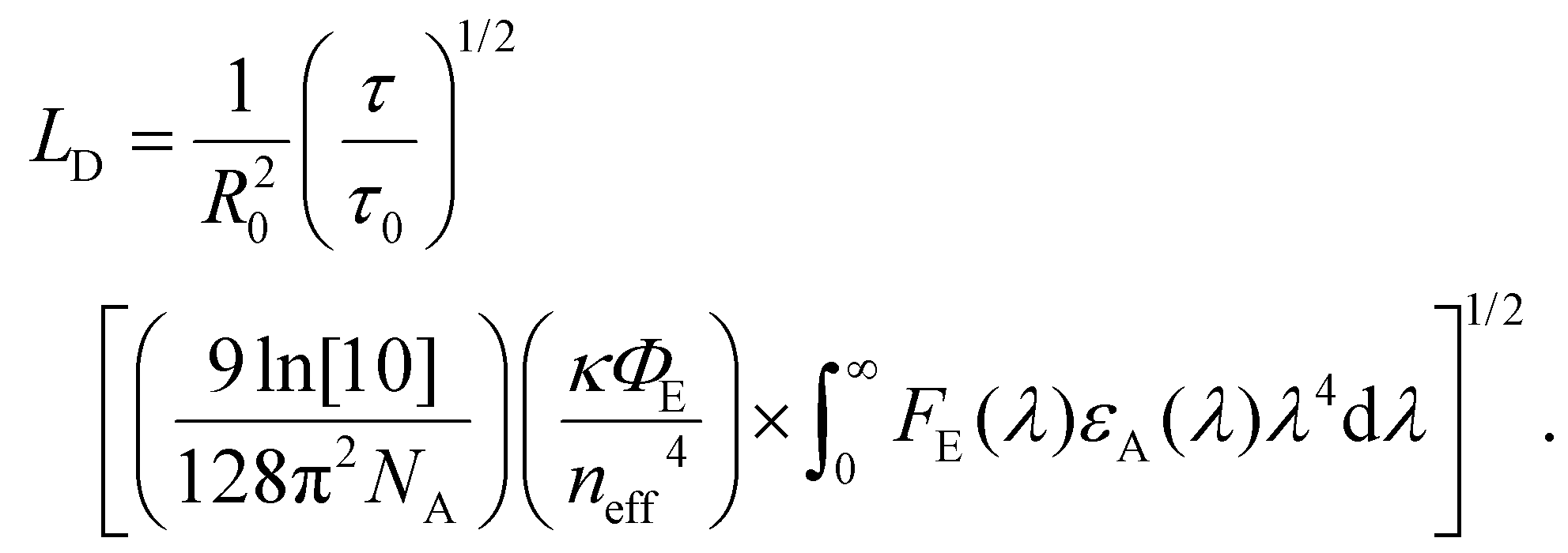 | (7) |
This treatment allows for the determination of LD through measurement the optical constants, best achieved through an absorption measurement combined with an nk-finder analysis,14 the ratio of the film to lone emitter lifetime, the spectral photoluminescence, and the absolute PLQY of the film.
FRET analysis is the least sensitive to the effects of challenge (i) as εA and FE can be measured at low excitation density with an incoherent or continuous-wave light source; however, care must be taken when measuring τ and τ0. FRET analysis is highly sensitive to challenge (ii) as the ratio between the lifetime of the emitter, relevant to kFRET, and the film, relevant to diffusive transport, has a large effect on the determined LD. FRET analysis is mostly insensitive to challenge (iii) as there is no quenching involved; however, care must be taken when measuring lifetimes as outlined in challenge (ii). As it relates to challenge (iv), this analysis involves the combination of many disparate measurements. Careful examination of each measurement is required for an accurate result. In addition, eqn (2) and (7) may need to be modified when the size of the molecule becomes comparable to the intermolecular spacing, or the delocalization becomes large;42,95,96 indicating that FRET analysis is expected to give a lower limit to D or LD.
3.2 2D microscopy
Often referred to as a direct measurement of exciton diffusion since the 2D contour plots 2D microscopy produces help develop an intuitive understanding of the diffusion process. This class of techniques utilizes a 2D stage or galvanometric mirrors to measure the spatial extent of the photoluminescent or transient absorption signals resulting in 2D spatial plots at various delay times. By modelling the evolution of the Gaussian distribution of excitons convoluted with the laser spot researchers can extract the time evolution of the diffusion constant. This technique is unique in that it can be used to measure anisotropy in diffusion, albeit restricted to the sample plane.72,97,98The primary constraint with 2D microscopy imaging is that the spatial resolution is limited to the diffraction limit of the pump (and probe) light,97 although some cite a spatial resolution as low as 50 nm.98 These techniques have been used to measure singlet and triplet diffusion constants in single crystals of tetracene as low as 0.0014 cm2 s−1.98 However, even the lower limit of 50 nm is too large to accurately quantify the diffusion in disordered organic semiconductors utilized in OPV applications. These techniques are not immune to challenge (i), although the use of very thin films (<50 nm) can be used to mitigate this challenge. As these techniques do not require any form of quenching, they are immune to challenge (ii) and (iii); however, the detectivity of the apparatus can be limited as they must be performed at sufficiently low excitation fluence that EEA does not occur, particularly near the centre of the diffraction limited excitation profile. With regards to challenge (iv), the apparatuses are more complex and expensive than other experimental techniques, which additionally requires sufficient technological expertise to operate. In addition, to produce diffraction limited spot-sizes researchers often utilize an oil immersion objective lens which may not be compatible with all materials. However, the modeling and fitting of data, in the simplest cases, is relatively straightforward.
3.3 Static quenching methods
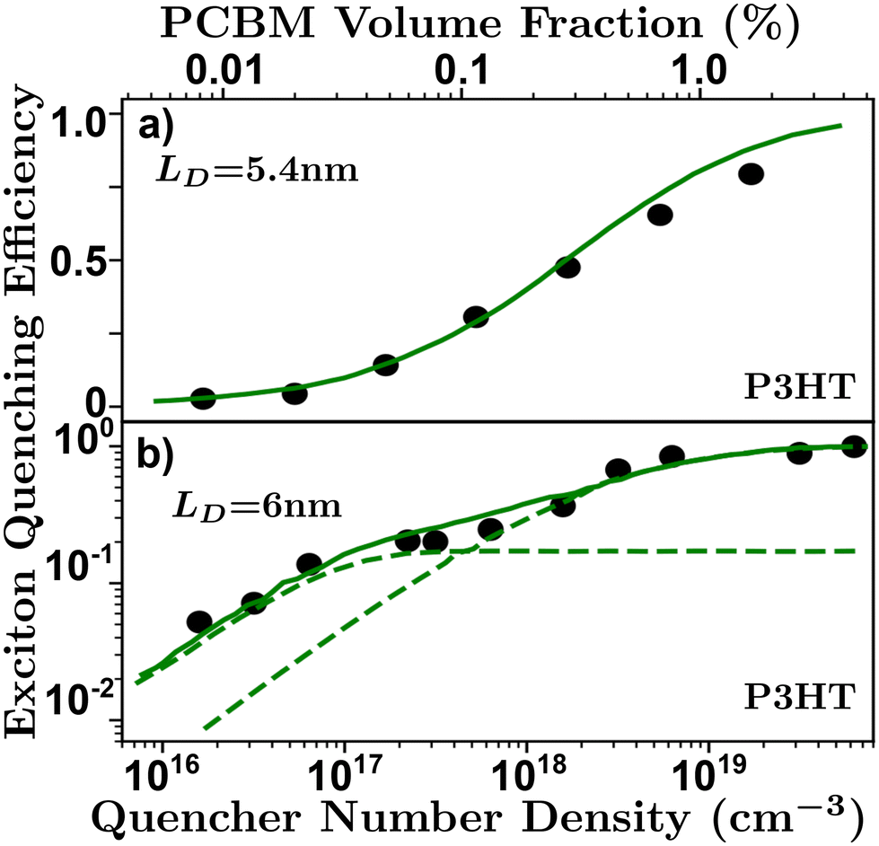 | ||
| Fig. 7 Volume quenching experiments in P3HT-RR.84 (a) Time-resolved photoluminescence experiments reveals a LD of 5.4 nm.52 (b) Anomalous quenching mechanism causing two quenching regimes revealing a LD of 6 nm with a 17% anomalous yield.34 | ||
The primary assumptions of volume quenching experiments are that there is a disperse and even distribution of quenching molecules throughout the film, which can only be determined by checking how well the model fits the data; an indication that the simulation accurately reflects the physical nature of the film.40,62,100 The pertinence of the model will depend on the range of quenching densities chosen for a given organic semiconductor.34 In addition, the initial distribution of excitons is sensitive to the optical properties of the film, especially in the case of electro-optical measurements requiring full-stack devices, making this technique especially sensitive to challenge (i).58,63 Challenge (ii) can strongly influence a volume quenching result if one is using the lifetime or integrated time-resolved emission as a measure of quenching efficiency in the ways described in challenge (ii). This is amplified when attempting to evaluate small differences at low quenching volumes where inaccuracies in the measurement of the lifetime can be caused by annihilation processes or long-range quenching.34,52 As discussed above, and illustrated in Fig. 6, there is some ambiguity in the spatial extent of the exciton and/or influence of the quenching molecule which leads to underestimations as described in challenge (iii). Volume quenching is sensitive to challenge (iv) in that care must be taken to correctly model the effect of the quenching molecule on the exciton given the range of measured density.40,52,58,64
The sample fabrication in bilayer quenching is very involved as it will inevitably require very thin samples which can be challenging to both fabricate and confirm the thickness of. As the accuracy of this technique relies on the measurement of the thickness of the excited layer it is important that researchers measure this accurately and with appropriate error attached, spectroscopic ellipsometry of films on silicon substrates yields the most accurate results of thickness.14,36 Additionally, the reproduction of pinhole-free samples with sharp interfaces can be very difficult. However, the innovation of the water-transfer method allows for the processing of very sharp bilayers and may help mitigate this difficulty in the future.29,36,62,101
With regards to challenge (i), the additional layer required can compound the optical interference effects when compared to volume quenching. For example, changing bilayer thicknesses can lead to differential light outcoupling between samples.62 This issue is illustrated in Fig. 5(b) and (c), where the optical interference pattern is simulated for a Y6 film on glass and a Y6 bilayer made with PM6, respectively, using input optical constants measured through a nk-finder analysis. In the exemplar wavelengths shown, the distribution of photogenerated excitons is different between the two cases. Accounting for this uneven distribution in a bilayer can be challenging without resorting to kMC modelling.62 As the models employed in bilayer quenching typically have LD as the only fitting parameter this measurement is immune to challenge (ii). Unless kMC is used to model quenching effects more accurately, in which case τ is typically required as an input parameter. However, to convert to D would require a measure of τ through eqn (4). The arguments attributed to challenge (iii) for volume quenching are equally applicable to bilayer quenching. In addition, the choice of material for the quenching layer can have a large effect on the resultant diffusion length,35,62,78 while the effect of FRET may be pronounced in bilayers due to geometrical effects.102 As discussed, the most technically demanding part of bilayer quenching experiments, and most relevant to challenge (iv), is the sample preparation and verification of the film thickness, especially when fabricating pinole-free films <25 nm in thickness.
To conclude section 3.3, and with respect to challenge (iii) and Fig. 6, static quenching experiments such as bilayer and volume quenching are most likely to underestimate LD in organic semiconductors.
3.4 Exciton–exciton annihilation
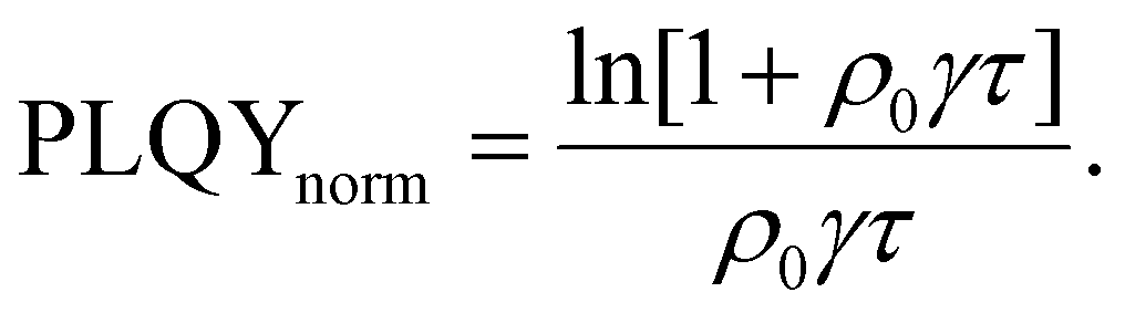
EEA techniques involve excitation of a thin film with an ultrafast pulsed laser to a high enough excitation density where EEA processes will dominate eqn (5) and comparing to a low excitation density case in the same film. With regards to challenge (i), one primary assumption of EEA is that the initial distribution of excitons is dispersed, both laterally across the film and into the film. However, as shown in Fig. 5(a), this assumption is not always valid. To keep the excitation profile into the film flat, researchers utilize very thin samples (<50 nm) and tune the excitation wavelength to match a low absorption wavelength of the sample.61 However, this can compound challenge (ii) as the pump power used for low-density excitation must be very small while thin samples have low overall absorption leading to a low photoluminescence or transient absorption signal and, therefore, low signal-to-noise. As EEA is a self-quenching mechanism, a major advantage over the static quenching experiments is that EEA experiments can be performed on a single film and do not require assumptions about dispersed quenching molecules or a sharp quenching interfaces. However, as the excitons are most likely delocalized, there is still a question of what length scale annihilation occurs over and hence challenge (iii) is not completely overcome. This length is known as the annihilation radii, as expressed in eqn (6), and its influence will become apparent. With regards to challenge (iv), the sample preparation is greatly simplified compared to static quenching experiments, and these techniques have been used to compare different deposition strategies.36,69 However, there are typically very expensive and highly technical apparatuses required to resolve the picosecond timescales over which annihilation occurs, the final technique named pulsed-PLQY partially overcomes this issue. | (8) |
Researchers begin by measuring τ at low densities, followed by multiple experimental runs varying ρ0 to gain information about γ from which D and LD can be calculated through eqn (4) and (6). This is achieved either by linearizing eqn (8) using exp[t/τ] or globally fitting eqn (8) for various ρ0, both of which require a measure of τ. However, the choice of which and how many densities to utilize adds additional experimental uncertainty and rigorously justifying the choice of densities is not easy. Too many decays with low (high) density will effectively weight a global fitting algorithm to the low (high) density case where τ(γ) is dominant, while the linearization is often averaged leading to an analogous effect. To illustrate this Fig. 8(a) shows linearized time resolved EAA results simulated using kMC. On a log–lin scale the effect of EEA is evident in the downturn at short timescales, most noticeable at high excitation densities. In the case of low excitation density, a fitting algorithm will express this downturn below the resolution of the experiment (or simulation), equivalent to very fast diffusion and annihilation, resulting in a larger estimation of γ and therefore LD at low excitation densities. This leads to an excitation dependent measure of D and LD.48,68,74 This effect can be seen in Fig. 8(b) where measured and simulated values of γ from literature are plotted against the initial exciton density for various time-resolved EEA studies. The x's indicate simulated data from the kMC simulations in Fig. 8(a), the circles indicate data digitized directly from the relevant references, while the squares indicate data that was digitized and re-analyzed. Note that this reanalyzed data was then scaled to the reported value in the reference (given by the dashed lines), as digitizing and reanalyzing data comes with many difficulties including unknown experimental parameters.
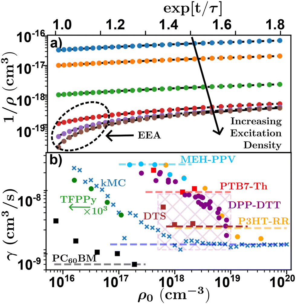 | ||
| Fig. 8 Density dependence of time-resolved exciton–exciton annihilation experiments. (a) Simulated linearized kMC experiments for various excitation densities indicating the effect of annihilation at high excitation densities. (b) Excitation density dependence of annihilation coefficient for various systems. Crosses-kMC simulations,48 circles-data digitized directly,48,68,74,75 squares-data digitized and re-alanyzed.66,71,103 Dashed lines indicate the reported value from literature, values for DPP-DTT was reported for a range of experiments indicated by the cross-hatched area. Chemical definitions are listed in Notes and references.84,99,104–108 | ||
Fig. 8(b) shows that as excitation density increases γ (as well as D and LD) asymptotically tend towards a saturated value.48 As a result of this, temporal-EEA techniques will tend to overestimate the value of diffusion length as low-density data will increase the extracted value of γ and hence, LD. One solution researchers use to control for this effect is to evaluate γ and for each chosen ρ0 to ensure that the chosen ρ0 are within the saturated regime and assign their error with respect to the density dependence of γ.48,74,75 However, high excitation densities can lead to photooxidation in most organic semiconductors which can be partially mitigated with a nitrogen rich environment.53 Researchers must take care to ensure that the excitation density is both within the saturation regime and not causing irreversible damage to the sample through photooxidation. Note that balancing the density dependence of γ with photooxidation is compounded in systems with small LD as the chosen densities must satisfy 1/ρ0 ≪ γτ to be in the saturated regime.48
In general, utilizing thin films and tuning excitation wavelengths can help alleviate challenge (i) through creating flat excitation profiles. However, the high initial excitation densities and small laser spot-sizes required (∼50 μm radius) indicate that the assumption of a laterally even distribution of excitons is spurious, resulting in areas of higher density that will artificially inflate the measured γ and LD. Challenge (ii) is compounded in these experiments as knowledge of τ is required to fit (8) irrespective of fitting technique. Inaccuracies in τ will lead not only to inaccuracies in the fitting, but also the calculation of LD through eqn (4). With regards to challenge (iii), the annihilation radius required to calculate D is an unknown quantity. Interesting studies have attempted to compare bilayer and EEA quenching experiments to determine this quantity and found that it is very similar to the intermolecular (π–π) sacking distances measured via grazing-incidence soft X-ray scattering,57 corroborating that EEA is a diffusion limited process for excitons delocalized over a few molecules. However, as discussed in section 3.3.2, the uncertainty in bilayer quenching experiments is not well defined and could be as large as the intermolecular spacing. Still many researchers choose to use the π–π stacking distances as an indicator of Ra, while others choose to assume only the order of magnitude to be nm. A precise technique for measuring Ra free from the challenges laid out above would be of great interest to the community and could shed light on the question of exciton delocalization. In the meanwhile, we recommend that Ra should be considered the largest source of uncertainty in these measurements and must be propagated accordingly. With regards to challenge (iv) the technical requirements for these experiments are concentrated in the apparatus itself. These experiments require a femtosecond source and picosecond resolution as the annihilation processes occur over picosecond timescale in organic semiconductors relevant to OPV research.
 | (9) |
Researchers measure the change in PLQY as a function of ρ0 over many orders of magnitude and fit to eqn (9) to extract the product of γτ and use eqn (4) and (6) to evaluate LD and, subsequently, D through a measure of τ. However, the analysis above does not account for exotic annihilation processes33 and is not sensitive to temporal dependent diffusion as described in the general case of eqn (6) or seen in thermally activated delayed fluorescence materials.110Fig. 9 shows data taken from a P3HT-RR film and the relevant fit, where LD was found to be 8 nm.
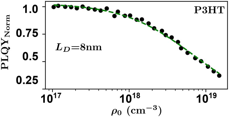
As pulsed-PLQY integrates over the temporal dynamics the spot-size does not need to be small, as is required for time-resolved EEA techniques. Therefore, the laser spot can be expanded which increases the validity of the assumption of a laterally even distribution of excitons.48 In addition, the effect of photooxidation can be readily checked during the experimental procedure by retracing a low density to high density experiment and comparing to the forward-scan case.48 Unique in EEA experiments, challenge (ii) is eliminated in the case of reporting LD, as it takes the opposite approach to time-resolved EEA techniques. First LD is measured without the need for a measure of τ, then, if desired, τ can be measured to calculate D through eqn (4). However, with regards to challenge (iii) all the uncertainty in Ra remains and researchers must consider this uncertainty carefully, as with time-resolved EEA techniques. Although pulsed-PLQY has only been demonstrated using a femtosecond excitation source it does eliminate the requirements for picosecond detection as normalized PLQY, and therefore LD, can be measured with any spectrally relevant photodiode, while τ can be measured via TRPL with lower resolution, greatly reducing the equipment cost and technical expertise required; therefore, partially improving on challenge (iv) from the time-resolved EEA case.
4 Discussion
Fig. 10 summarizes the findings of this perspective. Reported measurements of LD for various organic semiconductors are plotted for different measurement techniques described above. Note that this data has been taken directly from sources reporting but scaled to eliminate any differences in dimensionality or assumptions about Ra inherent in eqn (4) and (6). This is an important consideration when comparing across studies as simply comparing different definitions of eqn (4) could result in up to a factor of between reported values while different assumptions about Ra in eqn (6) for a given organic semiconductor can lead to disparate reports of LD. Note that Fig. 10 is not meant as a comprehensive review of all measurements of LD but rather a subset chosen with experimental comparison in mind.
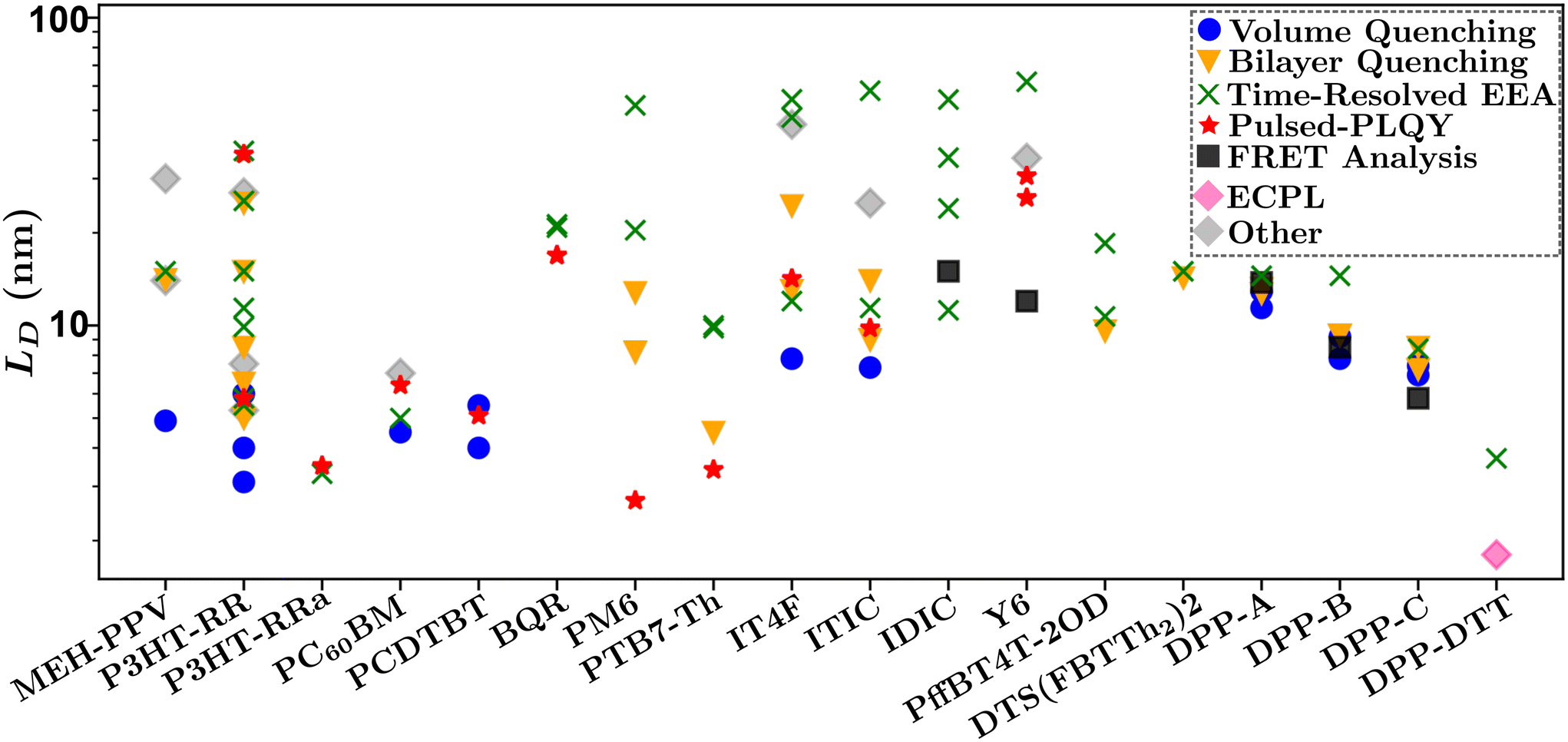 | ||
| Fig. 10 Comparison of reported values of LD for various systems and measurement techniques. Chemical definitions are listed in Notes and references.79,83,84,99,104–106,108,111–120 Data for each material was taken from references: MEh-PPV,56,64,88 P3HT-RR,34,35,48,52,54,58,61,65,67,86,87,90,94,100,121 P3HT-RRa,48,65 PCBM,34,48,66,91 PCDTBT,34,45,48 BQR,36,69 PM6,29,30,47,48,70 PTB7-Th,48,59,71,76 IT4F,48,50,57,62,76 ITIC,48,57,62,76 IDIC,42,70,76,122 Y6,36,44,48,72,76 DPP-A,51 DPP-B,51 DPP-C,51 DPP-DTT,68 PffBT4T-2OD,60,73 DTS(FBTTh2)2.103 | ||
In Fig. 10 there is a large spread of measurements within various organic semiconductors which can partially be explained by factors that are difficult to control for such as deposition conditions and variations in molecular weight.45,121 This is exemplified when comparing the other organic semiconductors in Fig. 10 to DPP-A,117 DPP-B,118 DPP-C,119 DPP-DTT,106 and DTS(FBTTh2)2,108 for which measurements on each material are taken from the same reference and show the smallest spread in values.51,68
Despite the spread in values, interesting observations can be drawn from this analysis. The first is that the volume and bilayer quenching experiments tend to report smallest values of LD. As outlined in section 3.3 and challenge (iii), and illustrated in Fig. 6, this is likely due to the systematic underestimations of quenching distances and hence LD. Further, volume quenching methods report lower values than bilayer quenching methods in all materials where the comparison is possible. This observation is not readily explained by the arguments in section 3.3 but indicates that there could be additional systematic underestimations in the effect of quenching centers on the electrostatics of the surrounding media.81 The second observation is that time-resolved EEA techniques tend to report the largest values of LD, and tend to have the largest spread in values when comparing within a single organic semiconductor. Both these results are explained by the excitation dependence of γ as shown in Fig. 8(b). The former is explained by the fact that γ will asymptotically approach a constant measure of LD with increasing excitation density, indicating that researchers are most likely to overestimate LD using time-resolved EEA due to low-density data inflating the measured value. The latter is explained as the choice of initial excitation density will affect the measured value, this is not typically considered or controlled for between various reported measurements. We advance pulsed-PLQY as a technique which can overcome many of the challenges posed in both time-resolved EEA and static quenching techniques. As seen in Fig. 10 pulsed-PLQY tends to provide intermediate measurements between these two extremes that is consistent with the high-density limit of time-resolved EEA.48 Pulsed-PLQY controls for challenge (i) though the use of a single thin film for measurements, challenge (ii) through the reporting of LD independent of measuring τ, challenge (iii) through the propagation of the uncertainty inherent in estimating Ra, and challenge (iv) through eliminating the requirement for multiple films with challenging deposition conditions and picosecond temporal resolution. In addition to pulsed-PLQY, other steady-state EEA techniques, such as ECPL, could also demonstrate similar benefits and seem to offer a lower limit to LD as seen in Fig. 10. Although the experimental setup for ECPL is significantly more complex than pulsed-PLQY.68
5 Conclusions
In conclusion, we examined the most widely used experimental techniques for evaluating exciton diffusion length in organic semiconductors. We systematically laid out the challenges inherent with each technique and provided insight into how the organic electronic community has worked to overcome these challenges.Our results show that, overall, static quenching experiments such as volume or bilayer quenching report the smallest values of diffusion length while time-resolved exciton–exciton annihilation techniques report the largest values. The former is due to uncertainties in the quenching distances between a mobile exciton and a static quenching molecule or layer, leading to underestimations of diffusion length. The latter is due to the techniques tendency to overestimate when using inappropriate experimental conditions. We advance that steady-state techniques, such as pulsed-PLQY, can overcome many of the challenges inherent in the other techniques. In general, the advancement of measurement techniques to accurately quantify exciton diffusion length in organic semiconductors has been decades in the making and these techniques are now being utilized by the wider organic semiconductor community. Care must be taken when choosing an experimental technique to utilize while appropriate understanding of the required apparatus, samples, experimental uncertainties, and limits of a technique is essential to collecting accurate measurements. It is the responsibility of the developers of these techniques to clearly define the scope, pitfalls, and applicability of each technique. We therefore intend this intervention to provide a framework for researchers to evaluate experimental results skeptically, to help interpret findings, and to aid researchers in establishing these techniques for themselves.
Author contributions
Drew B. Riley – conceptualization, methodology, software, formal analysis, investigation, data curation, writing – original draft, visualization. Paul Meredith – resources, writing – review and editing, supervision, project administration, funding acquisition. Ardalan Armin – writing – review and editing, supervision.Data availability
All data included in above submitted manuscript is available from the authors upon request or it is available from the citations where noted.Conflicts of interest
There are no conflicts to declare.Acknowledgements
This work was funded through the Welsh Government's Sêr Cymru II Program ‘Sustainable Advanced Materials’ (Welsh European Funding Office – European Regional Development Fund). P. M. is a Sêr Cymru II Research Chair and A. A. was a Rising Star Fellow also funded through the Welsh Government's Sêr Cymru II ‘Sustainable Advanced Materials’ Program (European Regional Development Fund, Welsh European Funding Office, and Swansea University Strategic Initiative). This work was also funded by the UKRI through the EPSRC Program grant EP/T028513/1 Application Targeted and Integrated Photovoltaics and the UKRI Research England RPIF Programme (Centre for Integrative Semiconductor Materials).References
- J. H. Davies, The physics of low-dimensional semiconductors: an introduction, Cambridge University Press, 1998. DOI:10.1017/CBO9780511819070.
- L. S. Xie, G. Skorupskii and M. Dinca, Chem. Rev., 2020, 120, 8536–8580, DOI:10.1021/acs.chemrev.9b00766.
- S. A. March, C. Clegg, D. B. Riley, D. Webber, I. G. Hill and K. C. Hall, Sci. Rep., 2016, 6, 39139, DOI:10.1038/srep39139.
- Q. Lin, A. Armin, R. C. R. Nagiri, P. L. Burn and P. Meredith, Nat. Photonics, 2015, 9, 106–112, DOI:10.1038/nphoton.2014.284.
- B. Kim, M. Kim, H. Kim, S. Jeong, J. Yang and M. S. Jeong, ACS Appl. Mater. Interfaces, 2022, 14, 35726–35733, DOI:10.1021/acsami.2c08680.
- D. Bera, L. Qian, T.-K. Tseng and P. H. Holloway, Materials, 2010, 3, 2260–2345, DOI:10.3390/ma3042260.
- A. Armin, W. Li, O. J. Sandberg, Z. Xiao, L. Ding, J. Nelson, D. Neher, K. Vandewal, S. Shoaee and T. Wang, et al. , Adv. Energy Mater., 2021, 11, 2003570, DOI:10.1002/aenm.202003570.
- P. W. Anderson, Phys. Rev., 1958, 109, 1492, DOI:10.1103/PhysRev.109.1492.
- A. Miller and E. Abrahams, Phys. Rev., 1960, 120, 745, DOI:10.1103/PhysRev.120.745.
- A. Köhler and H. Bässler, Electronic processes in organic semiconductors: An introduction, John Wiley & Sons, 2015. DOI:10.1002/9783527685172.
- M. S. Vezie, S. Few, I. Meager, G. Pieridou, B. Dörling, R. S. Ashraf, A. R. Goñi, H. Bronstein, I. McCulloch and S. C. Hayes, et al. , Nat. Mater., 2016, 15, 746–753, DOI:10.1038/nmat4645.
- J. Bertrandie, J. Han, C. S. De Castro, E. Yengel, J. Gorenflot, T. Anthopoulos, F. Laquai, A. Sharma and D. Baran, Adv. Mater., 2022, 34, 2202575, DOI:10.1002/adma.202202575.
- A. M. Kay, O. J. Sandberg, N. Zarrabi, W. Li, S. Zeiske, C. Kaiser, P. Meredith and A. Armin, Adv. Funct. Mater., 2022, 32, 2113181, DOI:10.1002/adfm.202113181.
- R. Kerremans, C. Kaiser, W. Li, N. Zarrabi, P. Meredith and A. Armin, Adv. Opt. Mater., 2020, 8, 2000319, DOI:10.1002/adom.202000319.
- A. Armin, D. M. Stoltzfus, J. E. Donaghey, A. J. Clulow, R. C. R. Nagiri, P. L. Burn, I. R. Gentle and P. Meredith, J. Mater. Chem. C, 2017, 5, 3736–3747, 10.1039/C7TC00893G.
- S. Athanasopoulos, E. V. Emelianova, A. B. Walker and D. Beljonne, Phys. Rev. B: Condens. Matter Mater. Phys., 2009, 80, 195209, DOI:10.1103/PhysRevB.80.195209.
- P. A. Hume, W. Jiao and J. M. Hodgkiss, J. Mater. Chem. C, 2021, 9, 1419–1428, 10.1039/d0tc05697a.
- D. Balzer and I. Kassal, J. Phys. Chem. Lett., 2023, 14, 2155–2162, DOI:10.1021/acs.jpclett.2c03886.
- A. J. Sneyd, T. Fukui, D. Paleček, S. Prodhan, I. Wagner, Y. Zhang, J. Sung, S. M. Collins, T. J. Slater and Z. Andaji-Garmaroudi, et al. , Sci. Adv., 2021, 7 DOI:10.17863/CAM.71186.
- J. Aragó and A. Troisi, Adv. Funct. Mater., 2016, 26, 2316–2325, DOI:10.1002/adfm.201503888.
- R. Binder, J. Wahl, S. Römer and I. Burghardt, Faraday Discuss., 2013, 163, 205–222, 10.1039/C3FD20148A.
- J. T. Willson, D. Balzer and I. Kassal, arXiv Preprint, arXiv:2308.13194, 2023, DOI:10.48550/arXiv.2308.13194.
- S. Giannini, W.-T. Peng, L. Cupellini, D. Padula, A. Carof and J. Blumberger, Nat. Commun., 2022, 13, 2755, DOI:10.5281/zenodo.6406144.
- R. D. Jansen-van Vuuren, A. Armin, A. K. Pandey, P. L. Burn and P. Meredith, Adv. Mater., 2016, 28, 4766–4802, DOI:10.1002/adma.201505405.
- D. M. Stoltzfus, J. E. Donaghey, A. Armin, P. E. Shaw, P. L. Burn and P. Meredith, Chem. Rev., 2016, 116, 12920–12955, DOI:10.1021/acs.chemrev.6b00126.
- S. Karuthedath, J. Gorenflot, Y. Firdaus, N. Chaturvedi, C. S. De Castro, G. T. Harrison, J. I. Khan, A. Markina, A. H. Balawi and T. A. D. Peña, et al. , Nat. Mater., 2021, 20, 378–384, DOI:10.1038/s41563-020-00835-x.
- M. Stolterfoht, A. Armin, S. Shoaee, I. Kassal, P. Burn and P. Meredith, Nat. Commun., 2016, 7, 11944, DOI:10.1038/ncomms11944.
- T. M. Clarke and J. R. Durrant, Chem. Rev., 2010, 110, 6736–6767, DOI:10.1021/cr900271s.
- T. H. Lee, S. Y. Park, W.-W. Park, X. Du, J. H. Son, N. Li, O.-H. Kwon, H. Y. Woo, C. J. Brabec and J. Y. Kim, ACS Energy Lett., 2020, 5, 1628–1635, DOI:10.1021/acsenergylett.0c00564.
- K. Jiang, J. Zhang, Z. Peng, F. Lin, S. Wu, Z. Li, Y. Chen, H. Yan, H. Ade and Z. Zhu, et al. , Nat. Commun., 2021, 12, 468, DOI:10.1038/s41467-020-20791-z.
- R. Sun, J. Guo, Q. Wu, Z. Zhang, W. Yang, J. Guo, M. Shi, Y. Zhang, S. Kahmann and L. Ye, et al. , Energy Environ. Sci., 2019, 12, 3118–3132, 10.1039/C9EE02295C.
- M. B. Price, P. A. Hume, A. Ilina, I. Wagner, R. R. Tamming, K. E. Thorn, W. Jiao, A. Goldingay, P. J. Conaghan and G. Lakhwani, et al. , Nat. Commun., 2022, 13, 2827, DOI:10.1038/s41467-022-30127-8.
- J. M. Hodgkiss, S. Albert-Seifried, A. Rao, A. J. Barker, A. R. Campbell, R. A. Marsh and R. H. Friend, Adv. Funct. Mater., 2012, 22, 1567–1577, DOI:10.1002/adfm.201102433.
- N. Zarrabi, A. Yazmaciyan, P. Meredith, I. Kassal and A. Armin, J. Phys. Chem. Lett., 2018, 9, 6144–6148, DOI:10.1021/acs.jpclett.8b02484.
- Y. Wang, H. Ohkita, H. Benten and S. Ito, ChemPhysChem, 2015, 16, 1263–1267, DOI:10.1002/cphc.201402740.
- D. B. Riley, O. J. Sandberg, N. Zarrabi, Y. R. Kim, P. Meredith and A. Armin, Adv. Mater., 2023, 35, 2211174, DOI:10.1002/adma.202211174.
- A. J. Gillett, A. Privitera, R. Dilmurat, A. Karki, D. Qian, A. Pershin, G. Londi, W. K. Myers, J. Lee and J. Yuan, et al. , Nature, 2021, 597, 666–671, DOI:10.1038/s41586-021-03840-5.
- D. Lee, H. Hwang, D. H. Sin, C. Park, S. G. Han, J. Mun, J. Noh, S. H. Kim, H. Kim and H. Lee, et al. , ACS Energy Lett., 2021, 6, 2610–2618, DOI:10.1021/acsenergylett.1c01049.
- D. Lee, S. G. Han, H. Kim, H. Hwang, C. Park, J. Noh, J. Mun, H.-W. Nho, J. B. Cho and D. H. Kim, et al. , Chem. Mater., 2022, 34, 10873–10884, DOI:10.1021/acs.chemmater.2c02175.
- O. V. Mikhnenko, P. W. Blom and T.-Q. Nguyen, Energy Environ. Sci., 2015, 8, 1867–1888, 10.1039/C5EE00925A.
- O. V. Mikhnenko, M. Kuik, J. Lin, N. van der Kaap, T.-Q. Nguyen and P. W. Blom, Adv. Mater., 2014, 12, 1912–1917, DOI:10.1002/adma.201304162.
- S. Chandrabose, K. Chen, A. J. Barker, J. J. Sutton, S. K. Prasad, J. Zhu, J. Zhou, K. C. Gordon, Z. Xie and X. Zhan, et al. , J. Am. Chem. Soc., 2019, 141, 6922–6929, DOI:10.1021/jacs.8b12982.
- A. Classen, C. L. Chochos, L. Lüer, V. G. Gregoriou, J. Wortmann, A. Osvet, K. Forberich, I. McCulloch, T. Heumüller and C. J. Brabec, Nat. Energy, 2020, 5, 711–719, DOI:10.1038/s41560-020-00684-7.
- Y. Zhu, Z. Zhang, W. Si, Q. Sun, G. Cai, Y. Li, Y. Jia, X. Lu, W. Xu and S. Zhang, et al. , J. Am. Chem. Soc., 2022, 144, 12747–12755, DOI:10.1021/jacs.2c03161.
- M. Streiter, D. Beer, F. Meier, C. Göhler, C. Lienert, F. Lombeck, M. Sommer and C. Deibel, Adv. Funct. Mater., 2019, 29, 1903936, DOI:10.1002/adfm.201903936.
- S.-B. Rim, R. F. Fink, J. C. Schöneboom, P. Erk and P. Peumans, Appl. Phys. Lett., 2007, 91, 173504, DOI:10.1063/1.2783202.
- P. Xue, A. M. Calascibetta, K. Chen, K. E. Thorn, Y. Jiang, J. Shi, B. Jia, M. Li, J. Xin and G. Cai, et al. , J. Mater. Chem. A, 2022, 10, 24073–24083, 10.1039/D2TA07113D.
- D. B. Riley, O. J. Sandberg, W. Li, P. Meredith and A. Armin, Phys. Rev. Appl., 2022, 17, 024076, DOI:10.1103/PhysRevApplied.17.024076.
- M. T. Sajjad, A. Ruseckas and I. D. Samuel, Matter, 2020, 3, 341–354, DOI:10.1016/j.matt.2020.06.028.
- T. H. Lee, Y. Dong, R. A. Pacalaj, S. Y. Park, W. Xu, J.-S. Kim and J. R. Durrant, Adv. Funct. Mater., 2022, 32, 2208001, DOI:10.1002/adfm.202208001.
- J. D. Lin, O. V. Mikhnenko, J. Chen, Z. Masri, A. Ruseckas, A. Mikhailovsky, R. P. Raab, J. Liu, P. W. Blom and M. A. Loi, et al. , Mater. Horiz., 2014, 1, 280–285, 10.1039/c3mh00089c.
- O. V. Mikhnenko, H. Azimi, M. Scharber, M. Morana, P. W. Blom and M. A. Loi, Energy Environ. Sci., 2012, 5, 6960–6965, 10.1039/C2EE03466B.
- H. Gerischer and A. Heller, J. Phys. Chem., 1991, 95, 5261–5267, DOI:10.1021/j100166a063.
- H. Wang, H.-Y. Wang, B.-R. Gao, L. Wang, Z.-Y. Yang, X.-B. Du, Q.-D. Chen, J.-F. Song and H.-B. Sun, Nanoscale, 2011, 3, 2280–2285, 10.1039/C0NR01002B.
- A. J. Ward, A. Ruseckas and I. D. Samuel, J. Phys. Chem. C, 2012, 116, 23931–23937, DOI:10.1021/jp307538y.
- J. A. Bjorgaard and M. E. Köse, J. Appl. Phys., 2013, 113, 203707, DOI:10.1063/1.4807415.
- M. T. Sajjad, A. Ruseckas, L. K. Jagadamma, Y. Zhang and I. D. Samuel, J. Mater. Chem. A, 2020, 8, 15687–15694, 10.1039/D0TA06017H.
- C. Goh, S. R. Scully and M. D. McGehee, J. Appl. Phys., 2007, 101, 114503, DOI:10.1063/1.2737977.
- T. Zhang, D. B. Dement, V. E. Ferry and R. J. Holmes, Nat. Commun., 2019, 10, 1156, DOI:10.1038/s41467-019-09062-8.
- Y. Zhang, M. T. Sajjad, O. Blaszczyk, A. J. Parnell, A. Ruseckas, L. A. Serrano, G. Cooke and I. D. Samuel, Chem. Mater., 2019, 31, 6548–6557, DOI:10.1021/acs.chemmater.8b05293.
- P. E. Shaw, A. Ruseckas and I. D. Samuel, Adv. Mater., 2008, 20, 3516–3520, DOI:10.1002/adma.200800982.
- V. Belova, A. Perevedentsev, J. Gorenflot, C. S. De Castro, M. Casademont-Viñas, S. H. Paleti, S. Karuthedath, D. Baran, F. Laquai and M. Campoy-Quiles, Sol. RRL, 2022, 6, 2100822, DOI:10.1002/solr.202100822.
- S. R. Scully and M. D. McGehee, J. Appl. Phys., 2006, 100, 034907, DOI:10.1063/1.2226687.
- K. Kawata, V. Burlakov, M. Carey, H. Assender, G. Briggs, A. Ruseckas and I. Samuel, Sol. Energy Mater. Sol. Cells, 2005, 87, 715–724, DOI:10.1016/j.solmat.2004.07.046.
- H. Ohkita, Y. Tamai, H. Benten and S. Ito, IEEE J. Sel. Top. Quantum Electron., 2015, 22, 100–111, DOI:10.1109/JSTQE.2015.2457615.
- S. Cook, A. Furube, R. Katoh and L. Han, Chem. Phys. Lett., 2009, 478, 33–36, DOI:10.1016/j.cplett.2009.06.091.
- S. Cook, H. Liyuan, A. Furube and R. Katoh, J. Phys. Chem. C, 2010, 114, 10962–10968, DOI:10.1021/jp101340b.
- Y. Zheng, R. Venkatesh, E. Rojas-Gatjens, E. Reichmanis and C. Silva-Acuña, J. Phys. Chem. Lett., 2024, 15, 272–280, DOI:10.1021/acs.jpclett.3c03094.
- M. T. Sajjad, Y. Zhang, P. B. Geraghty, V. D. Mitchell, A. Ruseckas, O. Blaszczyk, D. J. Jones and I. D. Samuel, J. Mater. Chem. C, 2019, 7, 7922–7928, 10.1039/C9TC00951E.
- S. Y. Park, S. Chandrabose, M. B. Price, H. S. Ryu, T. H. Lee, Y. S. Shin, Z. Wu, W. Lee, K. Chen and S. Dai, et al. , Nano Energy, 2021, 84, 105924, DOI:10.1016/j.nanoen.2021.105924.
- S. Dai, S. Chandrabose, J. Xin, T. Li, K. Chen, P. Xue, K. Liu, K. Zhou, W. Ma and J. M. Hodgkiss, et al. , J. Mater. Chem. A, 2019, 7, 2268–2274, 10.1039/C8TA11637G.
- G. Morganti, L. Bolzonello, F. Bernal-Texca, J. Martorell and N. F. van Hulst, J. Phys. Chem. Lett., 2023, 14, 1999–2005, DOI:10.1021/acs.jpclett.2c03585.
- H. Cha, S. Wheeler, S. Holliday, S. D. Dimitrov, A. Wadsworth, H. H. Lee, D. Baran, I. McCulloch and J. R. Durrant, Adv. Funct. Mater., 2018, 28, 1704389, DOI:10.1002/adfm.201704389.
- A. Lewis, A. Ruseckas, O. Gaudin, G. Webster, P. Burn and I. Samuel, Org. Electron., 2006, 7, 452–456, DOI:10.1016/j.orgel.2006.05.009.
- X. Zhang, K. Geng, D. Jiang and G. D. Scholes, J. Am. Chem. Soc., 2022, 144, 16423–16432, DOI:10.1021/jacs.2c04742.
- Y. Firdaus, V. M. Le Corre, S. Karuthedath, W. Liu, A. Markina, W. Huang, S. Chattopadhyay, M. M. Nahid, M. I. Nugraha and Y. Lin, et al. , Nat. Commun., 2020, 11, 5220, DOI:10.1038/s41467-020-19029-9.
- B. Sun, N. Tokmoldin, O. Alqahtani, A. Patterson, C. S. De Castro, D. B. Riley, M. Pranav, A. Armin, F. Laquai and B. A. Collins, et al. , Adv. Energy Mater., 2023, 13, 2300980, DOI:10.1002/aenm.202300980.
- A. Haugeneder, M. Neges, C. Kallinger, W. Spirkl, U. Lemmer, J. Feldmann, U. Scherf, E. Harth, A. Gügel and K. Müllen, Phys. Rev. B: Condens. Matter Mater. Phys., 1999, 59, 15346, DOI:10.1103/PhysRevB.59.15346.
- Y6-2,2′-((2Z,2′Z)-((12,13-bis(2-ethylhexyl)-3,9-diundecyl-12,13-dihydro-[1,2,5]thiadiazolo[3,4-e]thieno[2′′,3′′:4′,5′]thieno[2′,3′:4,5]pyrrolo[3,2-g]thieno[2′,3′:4,5]thieno[3,2-b]indole-2,10-diyl)bis(methanylylidene))bis(5,6-difluoro-3-oxo-2,3-dihydro-1H-indene-2,1-diylidene))dimalononitrile.
- B. Masters, Eur. Phys. J. H, 2014, 39, 87–139, DOI:10.1140/epjh/e2013-40007-9.
- V. Stehr, R. F. Fink, B. Engels, J. Pflaum and C. Deibel, J. Chem. Theory Comput., 2014, 10, 1242–1255, DOI:10.1021/ct500014h.
- S. Chandrasekhar, Rev. Mod. Phys., 1943, 15, 1, DOI:10.1103/RevModPhys.15.1.
- PM6-poly[(2,6-(4,8-bis(5-(2-ethylhexyl-3-fluoro)thiophen-2-yl)-benzo[1,2-b:4,5-b′]dithiophene))-alt-(5,5-(1′,3′-di-2-thienyl-5′,7′-bis(2-ethylhexyl)benzo[1′,2′-c:4′,5′-c′]dithiophene-4,8-dione)].
- P3HT-RR-regioregular poly(3-hexylthiophene-2,5-diyl).
- BCP-eC9-[[12,13-bis(2-butyloctyl)-12,13-dihydro-3,9-dinonylbisthieno[2′′,3′′:4′,5′]thieno[2′,3′:4,5]pyrrolo[3,2-e:2′,3′-g][2,1,3]benzothiadiazole-2,10-diyl]bis[methylidyne(5,6-chloro-3-oxo-1H-indene-2,1(3H)-diylidene) ]]bis[propanedinitrile].
- G. Dicker, M. P. de Haas, L. D. Siebbeles and J. M. Warman, Phys. Rev. B: Condens. Matter Mater. Phys., 2004, 70, 045203, DOI:10.1103/PhysRevB.70.045203.
- J. E. Kroeze, T. J. Savenije, M. J. Vermeulen and J. M. Warman, J. Phys. Chem. B, 2003, 107, 7696–7705, DOI:10.1021/jp0217738.
- J. Toušek, J. Toušková, Z. Remeš, J. Čermák, J. Kousal, D. Kindl and I. Kuřitka, Chem. Phys. Lett., 2012, 552, 49–52, DOI:10.1016/j.cplett.2012.09.052.
- P. Urbánek, I. Kuřitka, S. Daniš, J. Toušková and J. Toušek, Polymer, 2014, 55, 4050–4056, DOI:10.1016/j.polymer.2014.05.054.
- C. Leow, T. Ohnishi and M. Matsumura, J. Phys. Chem. C, 2014, 118, 71–76, DOI:10.1021/jp4079376.
- M. C. Fravventura, J. Hwang, J. W. Suijkerbuijk, P. Erk, L. D. Siebbeles and T. J. Savenije, J. Phys. Chem. Lett., 2012, 3, 2367–2373, DOI:10.1021/jz300820n.
- C. Kaiser, S. Zeiske, P. Meredith and A. Armin, Adv. Opt. Mater., 2020, 8, 1901542, DOI:10.1002/adom.201901542.
- L. A. Pettersson, L. S. Roman and O. Inganäs, J. Appl. Phys., 1999, 86, 487–496, DOI:10.1063/1.370757.
- S. Cook, A. Furube and R. Katoh, Energy Environ. Sci., 2008, 1, 294–299, 10.1039/B805643A.
- Q. Guo, Y. Liu, M. Liu, H. Zhang, X. Qian, J. Yang, J. Wang, W. Xue, Q. Zhao and X. Xu, et al. , Adv. Mater., 2020, 32, 2003164, DOI:10.1002/adma.202003164.
- K. F. Wong, B. Bagchi and P. J. Rossky, J. Phys. Chem. A, 2004, 108, 5752–5763, DOI:10.1021/jp037724s.
- G. M. Akselrod, P. B. Deotare, N. J. Thompson, J. Lee, W. A. Tisdale, M. A. Baldo, V. M. Menon and V. Bulović, Nat. Commun., 2014, 5, 3646, DOI:10.1038/ncomms4646.
- Y. Wan, Z. Guo, T. Zhu, S. Yan, J. Johnson and L. Huang, Nat. Chem., 2015, 7, 785–792, DOI:10.1038/nchem.2348.
- PC 60 BM-bis(1-[3-(methoxycarbonyl)propyl]-1-phenyl)-[6,6]C62.
- L. Lüer, H.-J. Egelhaaf, D. Oelkrug, G. Cerullo, G. Lanzani, B.-H. Huisman and D. De Leeuw, Org. Electron., 2004, 5, 83–89, DOI:10.1016/j.orgel.2003.12.005.
- T. H. Lee, W.-W. Park, S. Y. Park, S. Cho, O.-H. Kwon and J. Y. Kim, Sol. RRL, 2021, 5, 2100326, DOI:10.1002/solr.202100326.
- S. R. Scully, P. B. Armstrong, C. Edder, J. M. Fréchet and M. D. McGehee, Adv. Mater., 2007, 19, 2961–2966, DOI:10.1002/adma.200700917.
- Y. Long, G. J. Hedley, A. Ruseckas, M. Chowdhury, T. Roland, L. A. Serrano, G. Cooke and I. D. Samuel, ACS Appl. Mater. Interfaces, 2017, 9, 14945–14952, DOI:10.1021/acsami.6b16487.
- meh-PPV-poly[2-methoxy-5-(2-ethylhexyloxy)-1,4-phenylenevinylene].
- PtB7-Th-poly[4,8-bis(5-(2-ethylhexyl)thiophen-2-yl)benzo[1,2-b;4,5-b′]dithiophene-2,6-diyl-alt-(4-(2-ethylhexyl)-3-fluorothieno[3,4-b]thiophene-)-2-carboxylate-2-6-diyl].
- DPP-DTT-poly[2,5-(2-octyldodecyl)-3,6-diketopyrrolopyrrole-alt-5,5-(2,5-di(thien-2-yl)thieno [3,2-b]thiophene)].
- TFPPy-1,3,6,8-tetrakis(4-formyl)phenylpyrene.
- DTS(FBTTh 2 )2-7,7′-(4,4-bis(2-ethylhexyl)-4H-silolo-[3,2-b:4,5-b′]dithiophene-2,6-diyl)bis(6-fluoro-4-(5′-hexyl-[2,2′-bithiophen]-5-yl)benzo[c][1,2,5]thiadiazole.
- R. Kepler, V. Valencia, S. Jacobs and J. McNamara, Synth. Met., 1996, 78, 227–230, DOI:10.1016/0379-6779(96)80143-3.
- K. Thakur, B. van der Zee, G.-J. A. Wetzelaer, C. Ramanan and P. W. M. Blom, Adv. Opt. Mater., 2022, 10, 2101784, DOI:10.1002/adom.202101784.
- P3HT-RaR-regiorandom poly(3-hexylthiophene-2,5-diyl).
- PCDTBT-poly[N-9′-heptadecanyl-2,7-carbazole-alt-5,5-(4′,7′-di-2-thienyl-2′,1′,3′-benzothiadiazole)].
- BQR-benzodithiophene-quaterthiophene-rhodanine.
- IT4F-3,9-bis(2-methylene-((3-(1,1-dicyanomethylene)-6,7-difluoro)-indanone))-5,5,11,11-tetrakis(4-hexylphenyl)-dithieno[2,3-d:2′,3′-d′]-s-indaceno[1,2-b:5,6-b′]dithiophene.
- ITIC-3,9-bis(2-methylene-(3-(1,1-dicyanomethylene)-indanone))-5,5,11,11-tetrakis(4-hexylphenyl)-dithieno[2,3-d:2′,3′-d′]-s-indaceno[1,2-b:5,6-b′]dithiophene.
- IDIC-2,2′-((2Z,2′Z)-((4,4,9,9-tetrahexyl-4,9-dihydro-s-indaceno[1,2-b:5,6-b′]dithiophene-2,7-diyl)bis(methanylylidene))bis(3-oxo-2,3-dihydro-1H-indene-2,1-diylidene))dimalononitrile.
- DPP-A-see ref. 51 for definition.
- DPP-B-see ref. 51 for definition.
- DPP-C-see ref. 51 for definition.
- PffBT4T-2OD-poly[(5,6-difluoro-2,1,3-benzothiadiazol-4,7-diyl)-alt-(3,3′′′-di(2-octyldodecyl)-2,2′;5′,2′′;5′′,2′′′-quaterthiophen-5,5′′′-diyl)].
- Z. Masri, A. Ruseckas, E. V. Emelianova, L. Wang, A. K. Bansal, A. Matheson, H. T. Lemke, M. M. Nielsen, H. Nguyen and O. Coulembier, et al. , Adv. Energy Mater., 2013, 3, 1445–1453, DOI:10.1002/aenm.201300210.
- H. Cha, Y. Zheng, Y. Dong, H. H. Lee, J. Wu, H. Bristow, J. Zhang, H. K. H. Lee, W. C. Tsoi and A. A. Bakulin, et al. , Adv. Energy Mater., 2020, 10, 2001149, DOI:10.1002/aenm.202001149.
| This journal is © The Royal Society of Chemistry 2024 |