
 Open Access Article
 This Open Access Article is licensed under a
 Creative Commons Attribution 3.0 Unported Licence
Laser-patterned epoxy-based 3D microelectrode arrays for extracellular recording†
Hu
Peng
 a,
Inola
Kopic
a,
Shivani Ratnakar
Potfode
a,
Tetsuhiko F.
Teshima
*ab,
George Al
Boustani
a,
Lukas
Hiendlmeier
a,
Chen
Wang
d,
Mian Zahid
Hussain
c,
Berna
Özkale
d,
Roland A.
Fischer
c and
Bernhard
Wolfrum
*ab
a,
Inola
Kopic
a,
Shivani Ratnakar
Potfode
a,
Tetsuhiko F.
Teshima
*ab,
George Al
Boustani
a,
Lukas
Hiendlmeier
a,
Chen
Wang
d,
Mian Zahid
Hussain
c,
Berna
Özkale
d,
Roland A.
Fischer
c and
Bernhard
Wolfrum
*ab
aNeuroelectronics, Munich Institute of Biomedical Engineering, Department of Electrical Engineering, TUM School of Computation, Information and Technology, Technical University of Munich, Hans-Piloty-Str. 1, 85748, Garching, Germany
bMedical & Health Informatics Laboratories NTT Research Incorporated, 940 Stewart Dr, Sunnyvale, CA 94085, USA
cChair of Inorganic and Metal–Organic Chemistry, School of Natural Sciences and Catalysis Research Centre, Department of Chemistry, Technical University of Munich, Lichtenbergstr. 4, 85748 Garching, Germany
dMicrorobotic Bioengineering Lab (MRBL), Department of Electrical Engineering, TUM School of Computation, Information, and Technology, Technical University of Munich, Hans-Piloty-Str. 1, Garching 85748, Germany
First published on 16th July 2024
Abstract
Microelectrode arrays are commonly used to study the electrophysiological behavior of cells. Recently, there has been a growing interest in fabricating three-dimensional microelectrode arrays. Here, we present a novel process for the fast fabrication of epoxy-based 3D microelectrode array platforms with the assistance of laser-patterning technology. To this end, we photopatterned 3D pillars as scaffolds using epoxy-based dry films. Electrodes and conductor traces were fabricated by laser patterning of sputtered platinum films on top of the 3D structures, followed by deposition of parylene-C for insulation. Microelectrodes at the tip of the 3D structures were exposed using a vertical laser ablation process. The final electrodes demonstrated a low impedance of ∼10 kΩ at 1 kHz in electrochemical impedance spectroscopy measurements under physiological conditions. We investigated the maximum compression force of the 3D structures, which could withstand approximately 0.6 N per pillar. The 3D microelectrode arrays were used to record extracellular signals from HL-1 cells in culture as a proof of principle. Our results show regular firing of action potentials recorded at the tip of the 3D structures, demonstrating the possibility of recording cell signals in non-planar environments.
1. Introduction
Monitoring the electrophysiological behavior of mammalian cells plays a crucial role in understanding various cellular processes, including communication, signaling, and metabolism.1,2 One popular tool for measuring electrophysiological activity within networks of cells is the microelectrode array (MEA).3–5 Nowadays, state-of-the-art planar MEAs can record network behavior in a label-free and real-time manner with thousands of channels in parallel.6,7 However, such devices may be unable to capture the electrophysiological behavior of cells not adjacent to the base substrate, for example, in 3D cultures. The demand for recording signals in non-planar topographies has led to the development of 3D MEAs.8–12 To this end, various fabrication technologies have been employed to fabricate 3D MEAs.13–16 For example, silicon-based 3D MEAs, such as the Utah array, are widely used in neural recording and stimulation applications.17 However, these 3D MEAs require a rigid silicon substrate,18 and the thickness of the substrate determines the height of the resulting 3D electrode. Additionally, the complex manufacturing process and high cost of silicon-based 3D MEAs can be prohibitive for some applications.19 Microwire 3D electrodes obtained by wire bonding provide a low-cost fabrication alternative.20 Yet, the exact feature size of individual 3D electrodes is typically difficult to control using this process. Inkjet, aerosol, and stereolithographic 3D printing methods offer a way to fabricate individual 3D electrodes for fast prototyping.21–27 However, some of these methods, such as inkjet printing, have limited patterning precision, and for others, scaling up the process for high-throughput production can be challenging.An alternative for fabricating 3D scaffold structures is based on photolithographically patterning solution-based SU-8, a commonly used negative photoresist with eight epoxy groups.28–30 Several examples of bioelectronic sensing devices based on thick epoxy photoresist platforms have been realized. Applications include local field potential recordings within brain tissues,31 single-cell analysis,32 and dopamine detection.33 However, to enable sensing using epoxy scaffolds, it is necessary to make the structures conductive. An established method to achieve this is to apply high-temperature pyrolysis to patterned SU-8 pillars.34 This process leads to carbonization and changes the height and diameter of the 3D structures significantly. During the process, other materials, such as metal feedlines, may be at risk of cracking in the furnace due to temperature-induced stresses. This can compromise the accuracy and reliability of the resulting sensing devices. In addition, solution-based SU-8 structures are sensitive to processing conditions.35,36 Instead, epoxy dry films consist of a cured modified epoxy formulation containing an antimony-free photo acid generator.37 It can be easily transferred and patterned in various thicknesses using standard UV lithography by avoiding processing liquid photoresist.38
In this report, we present a process for rapidly fabricating epoxy-based 3D MEAs using optical lithography combined with metal deposition and laser patterning. The generated 3D electrodes are insulated via parylene-C coating, enabling extracellular recording of action potentials from excitable HL-1 cells on the exposed pillars’ tips. We investigate the mechanical stability of the fabricated 3D structures using compression force measurements.
2. Experiments
2.1 Fabrication process of epoxy-based microelectrode arrays
SCHOTT AF 32® eco glass wafers (SCHOTT Glass Malaysia Components SDN BHD, Malaysia) with a diameter of 76.2 mm and thickness of 0.5 mm wafer were cleaned by subsequent ultrasonication (Bransonic ultra-sonic cleaner 5510E-MTH, Branson ultrasonic, Danbury, CT, USA) in acetone, isopropanol, and deionized water for 10 minutes each. Deionized water (conductivity 5.5 μS m−1) was taken from an ultra-clear purification system (Evoqua Water Technologies, Germany). Isopropanol (≥99.5%) and acetone (≥99.5%) were obtained from Carl Roth (Germany). The procedure was repeated twice, and afterward, the samples were blow-dried with compressed air. A dehydration bake of the wafer was then conducted at 70 °C for 15 minutes.SUEX series dry films (DJ MicroLaminates, Inc. USA) were used to generate the epoxy scaffold. The films were rolled onto the substrates at 70 °C using a manual laminating rubber roller (diameter 15 mm). A soft bake at 95 °C for 30 minutes was then carried out to adhere the films well onto the substrate. Photolithography was implemented using a maskless alignment system (μMLA, Heidelberg Instruments, Germany). A defocus of +10% (working distance 120 μm) with exposure doses of 18 J cm−2 was used (the wavelength of the light source was 365 nm). After exposure, the samples were subjected to a post-exposure bake by heating for 1 minute at 65 °C and then ramping up the temperature to 95 °C in 3 minutes. The temperature was kept at 95 °C for around 15 minutes and cooled to room temperature overnight to release the stress. The samples were then transferred to a beaker containing the developer (mrDev-600, micro resist technology GmbH, Germany), and development was performed with periodic shaking of the beaker for 20 minutes. Once the structures were visible, the samples were rinsed with isopropanol. The substrate was then transferred to another beaker containing the fresh developer and developed for approximately 30–40 seconds. Isopropanol was used again to rinse away any residues.
After epoxy pillars were formed on the glass wafer, metal layers (10 nm Ti followed by 100 nm Pt) were sputtered (BAL-TEC MED 020, BAL-TEC AG, Lichtenstein) onto the chip. A laser-patterning system (MD-U1000C, Keyence, Japan) was used to pattern the 3D MEAs by selectively ablating the metal film between individual electrode structures. Subsequently, 5 μm of parylene-C (PPS Parylene 3000, Plasma Parylene System GmbH, Germany) was deposited to passivate the entire chip. Finally, ring electrodes were exposed via vertically aligned laser ablation of the pillars’ tips (average laser power: 2.8 W, scan speed: 800 mm s−1, pulse frequency: 40 kHz, repetition: 30![[thin space (1/6-em)]](https://www.rsc.org/images/entities/char_2009.gif) 000).
000).
2.2 Structural characterization of epoxy-based 3D MEAs
Epoxy pillars were imaged with a 3D laser scanning confocal microscope (VK-X250, Keyence, Japan) to acquire the dimensions of the pillars. All measurements were run at a z-pitch of 80 nm.Scanning electron microscopy (SEM, TM-1000 tabletop SEM, Hitachi, Japan) was used to image the pillars. To this end, the MEAs were fixed onto a specimen holder and taped with conductive carbon cement (LEit-C-Plast, Neubauer Chemikalien, Germany). To prevent charging artifacts, a thin layer of gold (∼5 nm) was sputtered onto the sample using a high vacuum coating system (BAL-TEC MED 020, BAL-TEC AG, Lichtenstein) before loading the sample into the chamber.
For focus Ion Beam (FIB) milling and SEM imaging, the samples were fixed on holders with a conductive double-sided carbon pad and afterwards loaded into the FIB-SEM chamber (Gemini 2, Zeiss Crossbeam 550, Germany). The following settings were used for electrode milling and image acquisition: SEM beam voltage 1 kV, working distance 5 mm. The FIB Ga beam was accelerated at 30 kV with a current of 15 nA.
2.3 Mechanical characterization
Young's modulus of bare SUEX, SUEX/Pt, and SUEX/Au were measured via a tensile test device (Universal Testing Machines Model 106, TesT GmbH, Germany). The same device was used in compression mode to measure the force vs. displacement in the longitudinal direction of the pillar structures to assess the maximum compression force the pillars can withstand. A customized 3D printed holder (Ultimaker S3, Ultimaker, Netherland) was mounted to the device and attached to the planar MEA backside.2.4 Electrochemical characterization
Electrochemical impedance spectroscopy (EIS; 200 mV offset vs. Ag/AgCl, 10 mV amplitude, 1 Hz to 10 kHz scan range) was carried out using a VSP-300 potentiostat (Biologic Science Instruments, France) in a three-electrode configuration with an Ag/AgCl reference electrode (Dri-Ref, Flexref from World Precision Instrument, USA) and a coiled platinum wire as the counter electrode. The characterization experiments were conducted in phosphate-buffered saline (PBS). Before EIS, the 3D MEAs were activated in 150 mM H2SO4 using cyclic voltammetry (scan rate 500 mV s−1, −0.2 to 1.5 V vs. Ag/AgCl, 20 cycles).2.5 Recording in HL-1 cells
Cell culture materials and chemicals such as L-glutamine, fetal bovine serum, and penicillin/streptomycin were purchased from ThermoFisher Scientific (Waltham, MA, USA). Additionally, Cell culture flask, Claycomb medium, trypsin-EDTA solution, norepinephrine bitartrate, fibronectin, and gelatin were bought from Sigma-Aldrich (St Louis, MO, USA). HL-1 cells were cultured in Claycomb medium supplemented with 100 U mL−1 penicillin, 100 μg mL−1 streptomycin, 2 mM L-glutamine, 10% fetal bovine serum, and 0.1 mM norepinephrine in a cell culture flask. The cells were then incubated in a humidified chamber (CB210 CO2, Binder, Germany) at 37 °C with 5% CO2. Upon reaching confluency and exhibiting mechanical contractions, the cells were detached using a 0.05% Trypsin-EDTA solution and prepared for experimentation. 3D MEAs were sterilized by immersion in ethanol and treated with oxygen plasma (0.8 mbar, 80 W, 3 min; Diener Femto, Diener electronic, Germany) before cell seeding. After drying, the chips were incubated with a fibronectin solution (5 μg mL−1) and gelatin (0.2 mg mL−1) for approximately 1 hour at 37 °C. The protein solution was removed, and the chips were rinsed with Dulbecco's phosphate-buffered saline (PBS) (D8662, Sigma-Aldrich). HL-1 cells were seeded onto the chips with a concentration of 100 k cm−2, reaching confluency in about three days. The confluent cell layer was assessed using an inverted microscope (Axiovert 40 CFL, Carl Zeiss, Germany) with a 5× objective. The detection was performed with a 64-channel home-built amperometric amplifier system (10 kHz sampling rate per channel, 3.4 kHz bandwidth) in a two-electrode setup using a Ag/AgCl electrode as a combined reference and counter electrode.39 All the experiments were performed in a grounded Faraday cage. The cell activity was stopped by adding sodium dodecyl sulfate (SDS), 100 μL from 1 M stock solution pipetted into 1 mL medium on the chip, (Sigma-Aldrich, USA). Signal analysis was performed in MATLAB (MathWorks, MA, USA) as described previously.393. Results and discussion
A schematic of the epoxy-based 3D MEAs for electrophysiological recording and its fabrication process is shown in Fig. 1. A glass ring was used to maintain the medium for cell culture. Cells were grown on the surface of the 3D patterned microelectrode array, as shown in Fig. 1a. Exposed Pt pads were used to connect the MEA to an external multichannel amperometric recording system (Picoamp).39Fig. 1b illustrates the fabrication process of the epoxy-based 3D MEAs. Our process combines laser patterning and photolithography to fabricate an epoxy-based 3D micro-ring electrode array. In the first step, glass substrates were cleaned with acetone, isopropanol, and deionized water successively (Fig. 1(b, i)). Afterward, epoxy-based structures were directly fabricated on the substrate by optical lithography, as shown in Fig. 1(b, ii–iii). Subsequently, a layer of Ti followed by a layer of Pt was sputtered onto the sample (Fig. 1(b, iv)). The sputtering parameters were optimized to ensure a uniform coverage. This process metalized the entire chip surface, including the epoxy pillars. Laser-patterning was used to define the conductive traces and pads, and a chemically inert conformal layer of parylene-C was deposited via a CVD process to passivate the sample, see Fig. 1(b, v). Defined ring electrodes were generated at the tip of each 3D structure using a laser ablation process. To this end, we used a vertical chip arrangement that allows positioning and exposing the tip of the pillar perpendicular to the beam path of a laser-ablation system (Fig. 1(b, vi)).21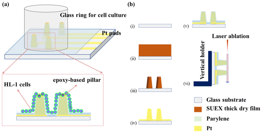 | ||
| Fig. 1 Schematic of the epoxy-based 3D MEAs for electrophysiological recording and illustration of the fabrication process. (a) Epoxy-based 3D MEAs for electrophysiological recording. (b) Fabrication process: (b, i) cleaned glass substrate, (b, ii) SUEX dry films laminated onto the cleaned substrate, (b, iii) epoxy pillars patterned by optical lithography, (b, iv) sputtered metal layer (Pt with a Ti adhesion layer) to cover the whole surface, (b, v) structuring of conductive traces and pads via laser patterning, passivation of structures by parylene-C, (b, vi) vertical laser-ablation to expose the ring electrode area at the tip of the epoxy-based microstructure. | ||
We obtained reproducible 3D structures based on the parameters described in the ESI (Fig. S1†). Fig. 2 shows a 3D profile analysis of the microelectrodes after laser ablation. In this study, we fabricated three different dimensions of epoxy pillars after laser ablation, with heights of 138.9 ± 9.9 μm, 171.6 ± 11.4 μm, and 234.0 ± 8.1 μm with an outer diameter of 116.2 ± 10.5 μm, 90.9 ± 3.4 μm, and 110.6 ± 16.1 μm, respectively (standard deviation was calculated from eight pillars from eight rows). Due to the ablation process, a ring electrode is formed at the pillar tip and contributes as an active area during electrochemical measurements. The samples we used for EIS and later cell measurements were fabricated from 200 μm thick films, resulting in a pillar height of ∼172 μm after laser ablation. We calculated the exposed ring electrode area based on the equation:
| Aring = π (router2 − rinner2) |
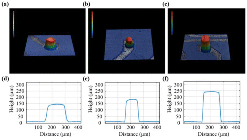 | ||
| Fig. 2 3D profile analysis of patterned microelectrodes. (a), (b) and (c) show 3D profiles of exemplary microelectrodes produced from different epoxy-based pillars’ layers captured via a 3D laser scanning confocal microscope. The scale bar for the height is shown at the top left of each image. The profiles were averaged from 6 directions and plotted in (d), (e), and (f). | ||
Fig. 3 shows the overview SEM image of epoxy-based pillars and their close-up images. As shown in Fig. 3(a and b), epoxy-based 3D structures were fabricated using optical lithography. After parylene passivation, tips were ablated to expose the ring electrode area for cell recording (see Fig. 3(c and d)). We performed FIB milling to expose a cross-section of an individual electrode, as shown in Fig. 3(e). It can be seen that a layer of ∼5 μm thickness parylene was uniformly coated on the surface of the pillar. The parylene coating on the substrate and on the pillar side wall exhibited no significant thickness difference. However, impurities, probably caused by the redeposition of ablated material, resulted in visible surface heterogeneities. Fig. 3(f) shows the overall layout of a single MEA. The MEA used in this study consisted of 64 electrodes fabricated on a glass substrate. The electrodes are arranged in a ∼3.6 × 3.6 mm2 pattern, with a center-to-center spacing of 508 μm. Each ring electrode is connected to a dedicated recording channel via a conductive trace (minimal width: 70 μm) routed on the substrate. These traces are insulated with a layer of 5 μm parylene to prevent electrical interference and cross-talk between adjacent channels. The design of the electrical routing ensures that signals from the electrodes reach the external data acquisition system with minimal distortion. Compared to conventional lithography, the resolution of our laser ablation technology is lower, limiting the reliable fabrication of features to ∼30 μm.
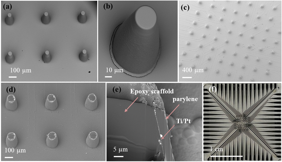 | ||
| Fig. 3 SEM images of micropillars and an optical image of the overall layout of the MEA. (a) An image of epoxy-based pillars, (b) a close-up image of an individual pillar, (c) epoxy-based 3D electrodes after laser ablation of the tips, (d) a close-up image of individual ring electrodes at the tip of the pillar. (e) A cross-sectional view of an individual pillar electrode obtained by focused-ion-beam milling. (f) An overall view of the MEA layout. | ||
Mechanical properties, such as Young's modulus of the dry films and its composites and the compression force of pillars, were studied further. We measured the compression force for different numbers of epoxy-based pillars with a height of 300 μm before parylene passivation. From this, we calculated the peak force per pillar until deformation occurred. An optical image of deformed pillars is shown in Fig. S2.† In addition, the Young's modulus of the bare SUEX dry films, SUEX/Pt, and SUEX/Au were measured (see Fig. S3†). To this end, we fixed our samples on a 3D-printed holder, which can be mounted to the load cell. To provide a uniform and flat contact interface, a glass slide was cleaned and placed on the bottom holder. The load cell was moving downwards with a steady speed of 5 mm min−1. Fig. 4(b) shows the distance vs. force curve for different numbers of pillars. The sample with 20 pillars exhibits a peak force of around 11.8 N, while the sample with 64 pillars has a peak force of around 38.5 N. Thus, the calculated force per pillar at which deformation occurs is approximately 0.6 N, independent of the pillar number. A high applicable force can be useful in potential applications, such as cantilevers for atomic force microscopes (AFM)40 and invasive neural recording.41
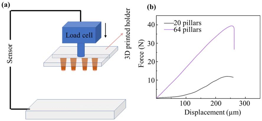 | ||
| Fig. 4 A schematic of the compression force measurement and resulting force-displacement curves. (a) The compression force measurement with a maximum load cell of 50 N, (b) force vs. displacement curves for different numbers of pillars. | ||
After exposing the pillars’ tips via laser ablation, EIS was carried out to characterize the electrode–electrolyte interface of the epoxy-based 3D MEAs. As expected, the impedance decreases with increasing frequency but does not follow a purely capacitive (1/f) relation. Specifically, at 1 kHz, the impedance is approximately 10 kΩ. This value is significantly lower than expected for a small exposed gold electrode of ∼28 μm2, assuming typical values for the specific interfacial capacitance between 20 μF to 40 μF per cm2. A possible reason for this deviation can be ascribed to the laser ablation process. While the parylene coating procedure typically ensures good insulation quality, after laser ablation, the ring electrode area may no longer be tightly surrounded by parylene (an SEM example is shown in Fig. S4†). Thus, the inner electrode shafts could be exposed to electrolyte via a nano- or microscale gap at the pillar tip. This would result in a larger effective electrode/electrolyte interface compared to a standard ring electrode. A similar concept has been previously exploited in cell recordings with nanocavity electrodes.42 In this approach, a gap between the electrode and insulation layer was designed to effectively decrease the impedance of electrodes with a small recording aperture. The decreased impedance resulted in extracellular recordings with an improved signal-to-noise ratio.
As a proof of principle for the functionality of the 3D MEAs, we recorded extracellular signals from HL-1 cells. The cell growth was observed for five days, and the medium was changed daily until confluency was reached (see Fig. S5†). Spontaneous action potentials recorded from 6 channels for a duration of one minute are shown in Fig. S6.† After another 10 s, the cell contractions were stopped by adding 1% SDS (see Fig. 5b). Before application of SDS, we observed a stable but phase-shifted beating frequency at ∼0.7 Hz across all channels. The recorded peak-to-peak current amplitudes ranged from around 60 to 200 pA. The difference in amplitudes recorded at different channels can be explained by variations in the junction resistance at the interface of individual cells and microelectrodes. Signal traces from a single channel are exemplary, shown in Fig. 5(c), and the average spike shape of all recorded spikes is shown in Fig. 5(d). The average noise was calculated by evaluating the root mean square (RMS) of the trace. A superposition of 12 spikes was shown in Fig. S7.† For the given channel, the RMS value was 24.2 ± 1.3 pA with a peak-to-peak amplitude of 363.5 ± 21.7 pA (approximate SNR of 15). This proof-of-concept experiment demonstrated the applicability of the 3D MEA for extracellular signal recording from cardiomyocyte cells.
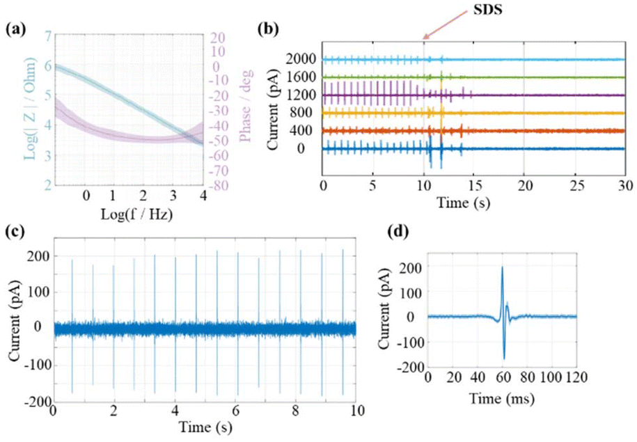 | ||
| Fig. 5 Impedance spectroscopy (EIS) characterization of epoxy-based 3D MEAs and signal recordings from HL-1 cells. (a) Average absolute impedance (blue) and phase (orange) were recorded from eight electrodes. (b) Spontaneous action potentials were recorded from 6 channels within the same cell culture. 1% SDS was added after 10 seconds to stop the electrical activity of the cells. For clarity, the individual curves have been shifted on the y-scale to a distance of 400 pA. (c) Current time trace of an extracellularly recorded cell signal for a single channel. The cells fire at a frequency of ∼0.7 Hz. (d) Average spike shape of all recorded spikes in the trace (±standard deviation). | ||
4. Conclusions
In this report, we introduced a process for rapidly fabricating 3D MEAs based on structured and metalized SUEX epoxy dry films combined with laser-patterning technology. We insulated the 3D structures with a parylene-C passivation layer and utilized laser ablation to refine the pillar tips. The functionality of the epoxy-based 3D MEAs was confirmed by EIS and recordings of extracellular signals from cardiomyocyte-like HL-1 cells at a distance of ∼172 μm from the base substrate layer. The pillars exhibit high stability, which could be advantageous for penetrating soft tissue for in vivo applications. While the structures presented are too large for localized recordings within small 3D cell assemblies, such as organoids, we believe the fabrication method can also be adapted to high-resolution 3D MEA platforms. This would open possibilities for potential applications in organoid and other 3D cell aggregate systems.Data availability
The data supporting this article have been included as part of the ESI.†Conflicts of interest
The authors declare that they have no known competing financial interests or personal relationships that could have appeared to influence the work reported in this paper.Acknowledgements
We greatly appreciate the financial support from the China Scholarship Council (CSC) and funding by the Federal Ministry of Education and Research (BMBF) and the Free State of Bavaria under the Excellence Strategy of the Federal Government and the Länder through the TUM Innovation Network: ARTEMIS and the ONE MUNICH Project Munich Multiscale Biofabrication. In addition, the authors thank Mrinalini Gupta for her help with the cell culture experiments.References
- M. Carter and J. C. Shieh, in Guide to Research Techniques in Neuroscience, ed. M. Carter and J. C. Shieh, Academic Press, New York, 2010, pp. 91–118. DOI:10.1016/B978-0-12-374849-2.00004-5.
- M. J. Zhu, H. M. Wang, S. Li, X. P. Liang, M. C. Zhang, X. C. Dai and Y. Y. Zhang, Adv. Healthcare Mater., 2021, 10, 21 Search PubMed.
- Y. Nam and B. C. Wheeler, Crit. Rev. Biomed. Eng., 2011, 39, 45–61 CrossRef PubMed.
- J. Müller, M. Ballini, P. Livi, Y. H. Chen, M. Radivojevic, A. Shadmani, V. Viswam, I. L. Jones, M. Fiscella, R. Diggelmann, A. Stettler, U. Frey, D. J. Bakkum and A. Hierlemann, Lab Chip, 2015, 15, 2767–2780 RSC.
- A. Casanova, L. Bettamin, M. C. Blatche, F. Mathieu, H. Martin, D. Gonzalez-Dunia, L. Nicu and G. Larrieu, J. Phys.: Condens. Matter, 2018, 30, 464001 CrossRef CAS.
- M. Ballini, J. Müller, P. Livi, Y. H. Chen, U. Frey, A. Stettler, A. Shadmani, V. Viswam, I. L. Jones, D. Jäckel, M. Radivojevic, M. K. Lewandowska, W. Gong, M. Fiscella, D. J. Bakkum, F. Heer and A. Hierlemann, IEEE J. Solid-State Circuits, 2014, 49, 2705–2719 Search PubMed.
- K. C. Kasuba, A. P. Buccino, J. Bartram, B. M. Gaub, F. J. Fauser, S. Ronchi, S. S. Kumar, S. Geissler, M. M. Nava, A. Hierlemann and D. J. Müller, Nat. Nanotechnol., 2024, 19, 825–833 CrossRef CAS.
- M. O. Heuschkel, M. Fejtl, M. Raggenbass, D. Bertrand and P. Renaud, J. Neurosci. Methods, 2002, 114, 135–148 CrossRef PubMed.
- D. A. Soscia, D. Lam, A. C. Tooker, H. A. Enright, M. Triplett, P. Karande, S. K. G. Peters, A. P. Sales, E. K. Wheeler and N. O. Fischer, Lab Chip, 2020, 20, 901–911 RSC.
- J. S. Choi, H. J. Lee, S. Rajaraman and D. H. Kim, Biosens. Bioelectron., 2021, 171, 112687 CrossRef CAS.
- O. Phouphetlinthong, E. Partiot, C. Bernou, A. Sebban, R. Gaudin and B. Charlot, Lab Chip, 2023, 23, 3603–3614 RSC.
- V. M. Eisenkolb, L. M. Held, A. Utzschmid, X. X. Lin, S. M. Krieg, B. Meyer, J. Gempt and S. N. Jacob, Cell Rep., 2023, 42, 112467 CrossRef CAS.
- M. Dimaki, P. Vazquez, M. H. Olsen, L. Sasso, R. Rodriguez-Trujillo, I. Vedarethinam and W. E. Svendsen, Sensors, 2010, 10, 10339–10355 CrossRef CAS.
- J. T. Robinson, M. Jorgolli, A. K. Shalek, M. H. Yoon, R. S. Gertner and H. Park, Nat. Nanotechnol., 2012, 7, 180–184 CrossRef CAS PubMed.
- K. Tasnim and J. Liu, J. Mol. Biol., 2022, 434, 167165 CrossRef CAS.
- M. A. Brown, K. M. Zappitelli, L. Singh, R. C. Yuan, M. Bemrose, V. Brogden, D. J. Miller, M. C. Smear, S. F. Cogan and T. J. Gardner, Nat. Commun., 2023, 14, 3610 CrossRef CAS PubMed.
- R. A. Normann and E. Fernandez, J. Neural Eng., 2016, 13, 061003 CrossRef PubMed.
- P. K. Campbell, K. E. Jones, R. J. Huber, K. W. Horch and R. A. Normann, IEEE Trans. Biomed. Eng., 1991, 38, 758–768 CrossRef CAS PubMed.
- M. S. Saleh, S. M. Ritchie, M. A. Nicholas, H. L. Gordon, C. S. Hu, S. Jahan, B. Yuan, R. Bezbaruah, J. W. Reddy, Z. Ahmed, M. Chamanzar, E. A. Yttri and R. P. Panat, Sci. Adv., 2022, 8, eabj4853 CrossRef CAS PubMed.
- P. Wijdenes, K. Haider, C. Gavrilovici, B. Gunning, M. D. Wolff, T. Lijnse, R. Armstrong, G. C. Teskey, J. M. Rho, C. Dalton and N. I. Syed, Sci. Rep., 2021, 11, 21952 CrossRef CAS.
- H. Peng, L. Grob, L. J. K. Weiss, L. Hiendlmeier, E. Music, I. Kopic, T. F. Teshima, P. Rinklin and B. Wolfrum, Nanoscale, 2023, 15, 4006–4013 RSC.
- S. Zips, L. Grob, P. Rinklin, K. Terkan, N. Y. Adly, L. J. K. Weiss, D. Mayer and B. Wolfrum, ACS Appl. Mater. Interfaces, 2019, 11, 32778–32786 CrossRef CAS.
- M. K. Saghafi, S. K. Vasantham, N. Hussain, G. Mathew, F. Colombo, B. Schamberger, E. Pohl, G. C. Marques, B. Breitung, M. Tanaka, M. Bastmeyer, C. Selhuber-Unkel, U. Schepers, M. Hirtz and J. Aghassi-Hagmann, Adv. Funct. Mater., 2024, 34, 2308613 CrossRef CAS.
- J. X. Jiang, X. Chen, Z. X. Mei, H. T. Chen, J. Y. Chen, X. Wang, S. F. Li, R. Y. Zhang, G. F. Zheng and W. W. Li, Micromachines, 2024, 15, 333 CrossRef.
- S. Zips, B. X. Huang, S. Hotte, L. Hiendlmeier, C. Wang, K. Rajamani, O. Buriez, G. Al Boustani, Y. Chen, B. Wolfrum and A. Yamada, ACS Appl. Mater. Interfaces, 2023, 15, 35950–35961 CrossRef CAS.
- J. Abu Shihada, M. Jung, S. Decke, L. Koschinski, S. Musall, V. R. Montes and A. Offenhaeusser, Adv. Sci., 2024, 11, 2305944 CrossRef CAS PubMed.
- M. A. Ali, C. S. Hu, E. A. Yttri and R. Panat, Adv. Funct. Mater., 2022, 32, 2107671 CrossRef CAS.
- S. C. Kilchenmann, E. Rollo, P. Maoddi and C. Guiducci, J. Microelectromech. Syst., 2016, 25, 425–431 Search PubMed.
- A. del Campo and C. Greiner, J. Micromech. Microeng., 2007, 17, R81–R95 CrossRef CAS.
- L. Amato, S. S. Keller, A. Heiskanen, M. Dimaki, J. Emneus, A. Boisen and M. Tenje, Microelectron. Eng., 2012, 98, 483–487 CrossRef CAS.
- G. Marton, G. Orban, M. Kiss, R. Fiath, A. Pongracz and I. Ulbert, PLoS One, 2015, 10, 380–383 Search PubMed.
- K. Keim, M. Z. Rashed, S. C. Kilchenmann, A. Delattre, A. F. Goncalves, P. Ery and C. Guiducci, Electrophoresis, 2019, 40, 1830–1838 CrossRef CAS.
- L. Amato, A. Heiskanen, C. Caviglia, F. Shah, K. Zor, M. Skolimowski, M. Madou, L. Gammelgaard, R. Hansen, E. G. Seiz, M. Ramos, T. R. Moreno, A. Martinez-Serrano, S. S. Keller and J. Emneus, Adv. Funct. Mater., 2014, 24, 7042–7052 CrossRef CAS.
- Y. M. Hassan, C. Caviglia, S. Hemanth, D. M. A. Mackenzie, T. S. Alstrom, D. H. Petersen and S. S. Keller, J. Anal. Appl. Pyrolysis, 2017, 125, 91–99 CrossRef CAS.
- D. H. Hwang, Y. C. Lo and K. P. Chin, Proc. SPIE, 2001, 4592, 131–139 CrossRef CAS.
- J. Liu, B. Cai, J. Zhu, G. Ding, X. Zhao, C. Yang and D. Chen, Microsyst. Technol., 2004, 10, 265–268 CrossRef CAS.
- D. Johnson, A. Voigt, G. Ahrens and W. Dai, 23rd International Conference on Micro Electro Mechanical Systems (MEMS), 2010, pp. 412–415.
- Y. Cao, J. Floehr, S. Ingebrandt and U. Schnakenberg, Micromachines, 2021, 12, 632 CrossRef PubMed.
- L. Grob, P. Rinklin, S. Zips, D. Mayer, S. Weidlich, K. Terkan, L. J. K. Weiss, N. Adly, A. Offenhausser and B. Wolfrum, Sensors, 2021, 21, 3981 CrossRef CAS PubMed.
- M. Hopcroft, T. Kramer, G. Kim, K. Takashima, Y. Higo, D. Moore and J. Brugger, Fatigue Fract. Eng. Mater. Struct., 2005, 28, 735–742 CrossRef.
- A. Altuna, J. Berganzo and L. J. Fernandez, Front. Mater., 2015, 2, 47 Search PubMed.
- B. Hofmann, E. Kätelhön, M. Schottdorf, A. Offenhäusser and B. Wolfrum, Lab Chip, 2011, 11, 1054–1058 RSC.
Footnote |
| † Electronic supplementary information (ESI) available. See DOI: https://doi.org/10.1039/d4nr01727g |
| This journal is © The Royal Society of Chemistry 2024 |