
 Open Access Article
 This Open Access Article is licensed under a
 Creative Commons Attribution 3.0 Unported Licence
Nanoscale, surface-confined phase separation by electron beam induced oxidation†
Sven
Barth
 *ab,
Fabrizio
Porrati
a,
Daniel
Knez
c,
Felix
Jungwirth
ab,
Nicolas P.
Jochmann
ab,
Michael
Huth
a,
Robert
Winkler
d,
Harald
Plank
cd,
Isabel
Gracia
e and
Carles
Cané
e
*ab,
Fabrizio
Porrati
a,
Daniel
Knez
c,
Felix
Jungwirth
ab,
Nicolas P.
Jochmann
ab,
Michael
Huth
a,
Robert
Winkler
d,
Harald
Plank
cd,
Isabel
Gracia
e and
Carles
Cané
e
aInstitute of Physics, Goethe University Frankfurt, Max-von-Laue-Str. 1, 60323 Frankfurt am Main, Germany. E-mail: barth@physik.uni-frankfurt.de
bInstitute for Inorganic and Analytical Chemistry, Goethe University Frankfurt, Max-von-Laue-Str. 7, 60438 Frankfurt, Germany
cInstitute of Electron Microscopy and Nanoanalysis, Graz University of Technology, Steyrergasse 17, 8010 Graz, Austria
dChristian Doppler Laboratory for Direct–Write Fabrication of 3D Nano–Probes (DEFINE), Institute of Electron Microscopy, Graz University of Technology, Steyrergasse 17, 8010 Graz, Austria
eInstitut de Microelectrònica de Barcelona (IMB), Centre Nacional de Microelectrònica (CNM), Consejo Superior de Investigaciones Científicas (CSIC), 08193 Barcelona, Spain
First published on 24th June 2024
Abstract
Electron-assisted oxidation of Co–Si-based focused electron beam induced deposition (FEBID) materials is shown to form a 2–4 nm metal oxide surface layer on top of an electrically insulating silicon oxide layer less than 10 nm thick. Differences between thermal and electron-induced oxidation on the resulting microstructure are illustrated.
Introduction
Maskless, site-selective writing of nanostructures of a desired shape and dimension using focused electron/ion beams is a powerful tool for controlled bottom-up nanofabrication.1–3 The unique 3D writing capabilities of these approaches allow tailoring of structures for the investigation of fundamental phenomena in diverse fields such as magnetism4,5 and optics.6,7 In addition, advances in the simulation of these printing processes provide guidance for optimized writing strategies8,9 and the ongoing development of precursors has expanded the range of available materials and compositions, thus broadening the potential application portfolio.10,11Besides studies of the fundamental properties of such as-grown nanostructures, there has been considerable interest in modifying the physical properties of materials prepared by focused electron beam induced deposition (FEBID). For instance, modification of the FEBID material has been achieved by post-growth processing such as electron beam curing (EBC) and the coating by chemical/physical vapour deposition of as-grown 3D FEBID nanostructures.12–15 The altered physical properties after post-growth treatments are typically attributed to changes in the microstructure of the FEBID material.16–18 This is indicative of the fact that these direct-write methods based on electrons and ions are non-equilibrium processes, which typically yield deposits in metastable states that can be driven towards equilibrium by post-growth treatments.19,20 Moreover, microstructures of as-grown FEBID materials frequently exhibit nanoscale phase separation due to the deposition of composite materials containing ligand fragments. Typically, metal-rich clusters form in a highly carbon-rich matrix, which leads to the electronic transport behaviour of nanogranular metals with (correlated) variable range hopping.21 Post-growth EBC can lead to grain growth of the metal nanoparticles by diffusion of either fragments caused by progressive decomposition of immobilized molecules or by electron-driven processes, within the deposited material, described in detail below.22 Hence, intentional changes of the microstructure and composition are of current interest for FEBID derived materials. For instance, the presence of water as a reactive gas during the EBC of FEBID-derived material can lead to pure noble metal or metal oxide nanostructures by oxidative removal of carbon impurities which is associated with the electron-induced formation of highly reactive hydroxyl radicals.23–25
In general, the energy range of the electrons causing microstructural and composition changes must be considered. For instance, metal surfaces can be oxidized under electron beam irradiation in the energy range of a few to hundreds of keV in the presence of oxygen or water.26–29 With respect to beam effects and reaction mechanisms in high energy processes one should always consider the effects of electron beam-induced atomic displacement as a cause for microstructural changes. This is of particular importance for in situ studies in transmission electron microscopes with primary electrons in the energy range of typically 200–300 keV. The atomic displacement is often considered as the main contribution for nanoparticle reorientation,30,31 re-crystallization,32 and enhancement of diffusion/sputtering processes.33,34 For studies in scanning electron microscopes, typically operating in the 5–30 keV energy range, atomic displacement is negligible. Other effects prevail as cause for microstructural changes and diffusion processes, such as electron beam heating, radiolysis, electrostatic charging, various ongoing energy-dependent bond cleavages etc.35 However, the assignment of a general dominant driving force for the microstructural changes during EBC of FEBID material in the SEM is not possible due to the complex interplay of different aspects to be considered. The complexity is caused by ill-defined bonding situations, low crystallinity as well as constituents of different atomic masses and reactivity within the deposits.
Naturally, the composition of FEBID and FIBID materials is dependent on the precursors used during the writing process. Bimetallic precursors are highly suitable model systems to gain insight into the FEBID growth process under specific growth conditions. In this respect, different fragmentation channels depending on the spatial distribution of high and low energy electrons driving the molecule fragmentation in single spot depositions have been suggested to be responsible for FeCo3 shell formation on an Fe-enriched NW core when HFeCo3(CO)12 is used as precursor.36 Typically, in monometallic precursors this effect is masked because the composition of the FEBID material varies only in the light elements originating from the ligands. Therefore, changes in the fragmentation behaviour or regimes are sometimes not obvious and easy to identify. In addition, the more complex bimetallic precursors allow a controlled deposition of materials with a specific, predefined metal ratio for a wide range of deposition parameters.22,37–39 Recently, we reported a single precursor source approach using H2Si(Co(CO)4)2 in FEBID to provide a dense material with a general composition of Co2SiCO.40 Such a deposit containing two metal/metalloid components with significantly different M–O bond energies is expected to be prone to phase separation under oxidizing conditions. The mostly amorphous Co2SiCO FEBID material with a low Co clustering tendency40 is expected to form SiO2 due to the high oxophilicity of Si and the Si–O bond strength of 452 kJ mol−1, which also surpasses the high Si–C bond strength of ∼300 kJ mol−1.41 The Co–O bond energy of ∼315 kJ mol−1 is also much lower than the energy gained by Si–O formation.42 Therefore, oxidative treatment of the materials will preferentially oxidize Si and lead to Si–O–Si bonding. Similarly, oxidation by thermal annealing of SiO2 covered Co2Si on Si results in continued SiO2 growth.43 Simultaneously with the oxidation of Si, Co is described to diffuse into the Si substrate material and thus the Si is progressively oxidized at the interface between Co2Si and the SiO2 top layer.43 This is a typical high temperature oxidation process involving solid state diffusion that can be carried out under wet and dry oxidizing conditions.44 Also, the Co2SiCO FEBID material is prone to diffusion processes changing the microstructure of the whole deposit with sufficient energy input as described below. It is therefore of interest to study electron-induced oxidation by EBC in the presence of small amounts of water as a mild modification that does not alter the bulk of FEBID material but only a small region near the surface.
Here we present a phase separation in the near-surface volume of FEBID materials driven by an electron-assisted oxidation process in the presence of small amounts of water. To the best of our knowledge, this is the first report of phase separation in a solid manifested by the formation of a surface-confined nanoscale bilayer structure composed of materials of different compositions. We demonstrate the differences in phase separation effects between thermally induced bulk diffusion and the highly surface sensitive electron driven process.
Results and discussion
Oxidative electron beam curing of Co2SiCO FEBID material
In a first step the Co2SiCO FEBID material was written using H2Si(Co(CO)4)2 as precursor as illustrated in the scheme of Fig. 1a and b. The further process step includes post-growth EBC in the presence of water, as schematically shown in Fig. 1b, resulting in the surface oxidation. Fig. 1c represents a cross-sectional view of as grown FEBID material and the assumed bilayer formation caused by phase separation after the oxidative EBC. The black box in the EBC treated material represents a part of the deposit typically presented in most of the figures of this paper. Fig. 1d shows a transmission electron microscopy (TEM) lamella prepared from an in-plane deposit with dimensions of 5 μm length and 1 μm width written on a SiO2 surface using e-beam parameters of 6.3 nA and 5 kV and post growth EBC with an electron dose of 1330 nC μm−2. The water in the residual background gas in SEM systems, even at low background pressures of ∼3.6 × 10⁻⁷ mbar,10,45 can be used for electron-induced oxidation. Dosing of additional water for oxidation is not required but an increased level was used for control experiments. When the samples were prepared for TEM, both a ∼3 nm Nb-based FEBID layer and an evaporated C layer were initially included to provide a distinct difference in contrast between the Co2SiCO FEBID and the envisioned phase separated material. Since excellent Z-contrast is provided by C alone, the Nb-based FEBID material has been omitted in most samples prepared for cross sections. For the TEM lamella preparation, the typical MeCpPtMe3-derived FEBID and FIBID PtCx protective layers were deposited on the surface prior to the cutting procedures. The deposited SiO2/Co2SiCO/NbNyCx/C/PtCx layer structure clearly contains at least one additional layer between the FEBID Co2SiCO and the NbNyCx/C top layer as shown in Fig. 1d. Close inspection reveals a very thin bright and dark line above the ∼100 nm thick Co2SiCO for the whole lamella length. A more obvious identification of two newly formed nanometric layers is illustrated in Fig. 1e. The contrast in the high-angle annular dark-field (HAADF) STEM image shows the formation of two layers below the dark C top layer and suggests a compositional variation that is more clearly seen in the energy dispersive X-ray (EDX) elemental maps for CoK and SiK. The initial Co2SiCO FEBID material is transformed into a Co-based top layer and a subsurface Si-based layer with a slightly higher Si concentration. The compositional variation is also illustrated in a line scan, which shows the layer formation and the extent of the transformation zone with a total depth of less than 15 nm. The EDX line scan reveals the aforementioned formation of oxides with increased O signals in the surface region. In addition, the ESI (Fig. S1†) includes a comprehensive set of elemental maps for a complete visual representation of the TEM lamella shown in Fig. 1. Additional examples of phase separation in different samples are also given in the ESI (Fig. S2 and S3†).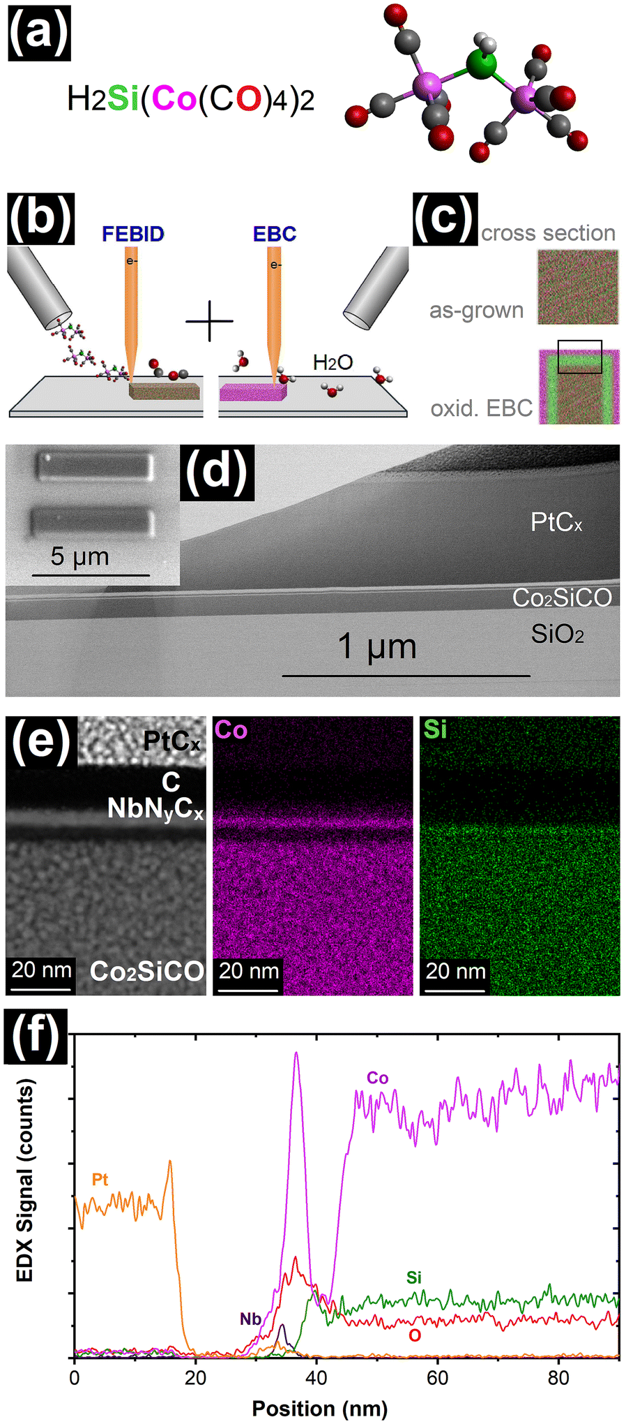 | ||
| Fig. 1 (a) Colorized sum formula and illustration of the H2Si(Co(CO)4)2 precursor used for FEBID. (b) The scheme illustrates FEBID writing and the following oxidative electron beam curing. (c) Schematic cross-sectional views of as-grown deposits and the anticipated oxidative conversion after EBC with phase separation in a Co-rich (pink) and Si-rich (green) layer are shown, which is also reflected in the (S)TEM images and EDX analyses thereafter. The black box represents the sections typically used for the TEM investigations. (d) BF STEM image of a cross-sectional lamella containing electron beam cured Co2SiCO FEBID written at 6.3 nA and 5 kV. EBC was carried out with an electron dose of 1330 nC μm−2. The inset shows a SEM image to illustrate the typical size of the FEBID structures. (e) The HAADF STEM image shows two new layers with different Z-contrast between the as-grown Co2SiCO FEBID in the lower part and the dark 10 nm C layer. The EDX CoK and SiK maps illustrate a newly formed Co-based layer separated from the initial FEBID material by a Si-based layer. (f) The graphical representation of a EDX line scan of the section shown in (e). | ||
The spatial confinement of the bilayer formation described in this study and illustrated in Fig. 1 and S1–S3† contrasts with the water-based purification of PtCx, which is a bulk effect in FEBID material up to ∼150 nm in depth and is not limited to a small near-surface region.46 One explanation for the different reaction volumes in the EBC would be a material dependent water penetration depth in the two FEBID materials. In this respect, it should be also noted that the electron penetration depth depends on the beam energy and the material composition. For 5 kV acceleration voltage, as used here, the penetration depth is in the range of hundreds of nm and cannot be the reason for the spatially confined reaction.47 While nanoscale phase separation in materials is commonly observed in the form of globular or nanolaminate inclusions in the bulk, as phase separation of eutectic compositions or as segregation at grain boundaries,48–51 the process of surface-bound nanoscale bilayer formation described herein appears to be very uncommon.
Further microstructural features of the Si and Co enriched layers have been investigated. Fig. 2a shows a bright field (BF) STEM image revealing the granular nature of the Co2SiCO FEBID material at the bottom with its corresponding fast Fourier transform (FFT) illustrating the amorphous nature as described in literature.40 As it can be expected due to the high crystallisation temperatures, the formed SiOx layer is amorphous and typically 6–8 nm thick. The cobalt oxide top layer is 2–3 nm thick and consists of individual nanocrystals, as shown by the individual FFT insets for different sections of the layer. The exact locations from which the FFTs originate are colour coded and indicated by horizontal lines, which also represent the edge length of the squares used for the FFTs. Accumulated information for a larger section of ∼25 nm edge length is shown in the FFT framed in orange. Similar examples for the crystalline nature of the cobalt oxide are presented in the ESI (Fig. S4†). The FFTs of several samples allowed the determination of CoO as the crystalline phase, which correlates well with the Co![[thin space (1/6-em)]](https://www.rsc.org/images/entities/char_2009.gif) :O atomic ratio shown in the EDX line scan of Fig. S3.†
:O atomic ratio shown in the EDX line scan of Fig. S3.†
 | ||
| Fig. 2 (a) BF STEM image of a TEM lamella of oxidative electron beam cured Co2SiCO FEBID material with an FFT inset on the lower right showing the mostly amorphous nature of the FEBID material. The crystalline cobalt oxide layer is 2–3 nm thick and reveals different crystallites. The FFTs originating from different positions along the layer illustrate the different orientations of the crystallites. The horizontal lines indicate the position from which the FFT originate, while the colour code matches location and FFT and the length of the horizontal lines provide the edge length of the squares used for FFTs. The frames for the FFTs contained also amorphous carbon originating from the protective layer, which does not affect the dot pattern. The STEM images show (b) a Co2SiCO NW section with corresponding EDX CoK and SiK maps and (c) a section treated by oxidative EBC using a higher electron dose of ∼4000 nC μm−2 to initiate the reaction. The more granular appearance in the HAADF image of the oxidative EBC treated NW indicates the onset of electron-induced bulk modification in addition to the oxidative phase separation on the surface. Radial EDX line scans of (d) an as-grown Co2SiCO FEBID NW section and (e) the oxidative EBC treated NW section show an expected accumulation of Co at the surface indicating the phase separation caused by the oxidative EBC (denoted by arrows and enlarged as an inset in (e)). | ||
The electron-induced oxidation and associated phase separation is not restricted to planar Co2SiCO deposits. Fig. 2b and d show the element distribution for an as-grown Co2SiCO nanowire (NW), illustrating the typical circular shape of FEBID NWs in the radial EDX line scan and the complete absence of phase separation. In contrast, oxidative EBC treated NWs reveal distinct changes in the microstructure (Fig. 2c and e). The accumulation of Co on the surface of the NW is clearly visible in the elemental CoK map of Fig. 2c and in the radial EDX line scan as small shoulders in the Co signal of Fig. 2e. The granular appearance in the HAADF STEM image of Fig. 2c indicates the onset of electron-induced bulk modification associated with the surface phase separation. We note that the oxidative EBC of the NWs typically results in bending of the nanowires and is more difficult to control than the process described above for the in-plane nanostructures. E.g., the electron dose had to be increased for similar beam parameters (5 kV; 6.3 nA; 4–6000 nC μm−2) in which case the EBC process also starts to affect the microstructure of the FEBID bulk. Specific tailoring of the process to such 3D NW structures is therefore required to realise the full potential of the here presented strategy.
Thermal oxidation and microstructure evolution of Co2SiCO FEBID material on microheaters
The FEBID process is not limited to specific substrate types. Therefore, in plane deposits on micromembranes with an integrated Joule heater52 have also been investigated to show possible differences in electron-induced and thermal oxidation behaviour. Schematically, the deposit location on micromembrane heaters as well as the two experiments at elevated temperatures described hereafter are shown in Fig. 3a–c. The thermal treatment was carried out in the SEM after the FEBID and under the same conditions as the electron-induced oxidation described above. Fig. 3d reveals significant dissimilarities between the EBC and thermal treatment in the SEM, as no specific tendency for Co enrichment at the surface but a Si termination can be observed for a thermal treatment at nominal ∼320 °C for 5 min. These results are similar to oxidation of Co2Si on SiO2 described in literature even though the oxidation temperatures are much higher for pure Co2Si.44 The formation of a SiO2 surface layer and Co enrichment in the remaining Co2Si have been observed akin to our results herein for the thermal treatment.44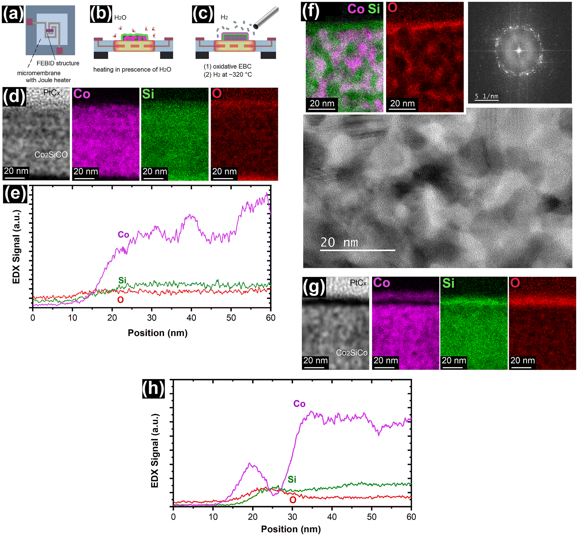 | ||
| Fig. 3 (a) Schematic illustration of micromembranes with integrated Joule heaters that have been used as substrates for FEBID. These platforms allowed the investigation of (b) thermal oxidation and diffusion of the FEBID material in the SEM and (c) the onset of reduction processes under hydrogen atmosphere. (d) The images show thermally oxidized Co2SiCO FEBID material by in situ heating to nominal ∼320 °C for 5 min using a micromembrane heater as illustrated in (b). The HAADF image shows the granular PtCx protective layer directly on top of the FEBID material, but the EDX CoK, SiK and OK maps reveal no surface accumulation of Co. (e) A graphical representation of a cross-sectional EDX of a 20 nm wide section taken at the center of (d). The onset of diffusion processes is indicated by the Co signal fluctuations. (f) Thermal treatment at nominally ∼350 °C for 5 min shows significant diffusion in the FEBID material, leading to crystallization of Co, evident in the BF STEM and the corresponding FFT, and the formation of a network. The phase separation and formation of SiOxCy is shown in the EDX CoK/SiK overlay and OK elemental map. (g) HAADF image and EDX CoK, SiK and OK maps of EBC oxidised Co2SiCO FEBID, followed by thermal reduction in 2 × 10⁻⁶ mbar H2 at nominal ∼320 °C for 5 min (as schematically shown in (c)). The images show the same information as Fig. 1e, but in the OK map a lower O concentration can be noted in the location of the phase separated Co, which can also be seen in (h) the graphical representation of a line scan EDX. Therefore, this result indicates the possibility of reduction of the cobalt oxide. | ||
Fig. 3b reveals fluctuations in the signal intensities for Co which indicates minor bulk diffusion processes within the FEBID material at ∼320 °C. Increasing the annealing temperature to nominal ∼350 °C results in a more significant surface oxidation and a discernible surface oxide that is rich in Si (Fig. 3c). In addition, a large rearrangement within the deposit is observed, which has also been described in the literature for other FEBID materials after thermal treatment.20,53,54 Thermally driven diffusion in metastable Co2SiCO FEBID material can be expected to result in a SiOxCy phase and metallic Co with potentially a low Si content. The overlay of SiK and CoK EDX maps shows this tendency, which is also supported by line scans as shown in Fig. S6.† In addition, the Co forms metallic nanocrystallites with predominantly hcp-Co phase. The bulk diffusion illustrates the limited thermal stability of the as-grown Co2SiCO FEBID material.
Thermal reduction of the top layer
In a final investigation, for the oxidative EBC treated and thus phase separated material, the reduction of CoO was investigated by thermal treatment in an H2 atmosphere at nominal 320 °C for 5 min using the micromembrane heater. The obtained material was subsequently covered with PtCx by FEBID to avoid reoxidation. Fig. 3d indicates the onset of reduction, as the OK map shows a low signal intensity for the Co layer, but neither electrical measurements nor FFT analyses provide evidence for metallic cobalt. Phase identification by diffraction does not allow the unambiguous allocation to a specific Co phase because the PtCx protective layer contains crystalline Pt nanoparticles, which tend to dominate the signal pattern in FFTs. Fig. S7 of the ESI† displays a four-terminal device prepared for electrical characterisation. However, no conductivity data for either hydrogen-treated or simply phase separated CoO/SiO2 layers could be recorded due to the high electrical resistance of the Co-based top layer. This high resistance can be attributed to either the low thickness of the cobalt-based layer or very high grain boundary resistances within the layer. In addition, it can be concluded, that the CoO/SiO2 bilayer provides electrical insulation between electron beam cured PtCx top electrodes and the conductive Co2SiCO FEBID bulk material.40Conclusions
Electron-driven, near-surface limited phase separation has been demonstrated for FEBID-derived Co2SiCO material as a consequence of post-growth electron beam curing. We consider the energetically preferred formation of a sub-surface amorphous SiOx layer through oxidation facilitated by hydroxyl radicals as a reason for the diffusion of cobalt to the surface. This phase separation results in the formation of a nanocrystalline CoO layer with a thickness of 2–4 nm and a total process depth of less than 15 nm. Similar observations have been made for 3D NWs, although the process control is more challenging. In contradistinction to the electron-driven reaction, thermally induced oxidation leads to silicon enrichment on the surface. Furthermore, the Co2SiCO FEBID material undergoes thermal diffusion at temperatures of approx. 320 °C, causing nano- to microscale phase separation to metallic cobalt and SiOxCy. The onset of thermally assisted reduction of cobalt oxide to Co in the presence of hydrogen was observed, but such thermal treatment at temperatures of approx. 320 °C already causes changes in the bulk microstructure of the FEBID material. Moreover, the Si-based sub-surface layer of approximately 8–10 nm acts as an electrical insulator for top-contact devices. To the best of our knowledge, this is the first observation of a surface-limited phase separation with one of the phases accumulating at the top surface. This process is expected to be universal for FEBID metal silicides and may provide a method of forming nanoscale metal oxide layers on top of a thin insulating SiO2 electrical barrier.Methods
FEBID
The synthesis of H2Si(Co(CO)4)2 was carried out by salt elimination using H2SiI2 and Na[Co(CO)4], similar to a published procedure55 and described in detail in a recent paper.39FEBID was performed using a dual beam SEM/FIB (FEI, Nova NanoLab 600) equipped with a Ga ion source. The home build gas injection system provided the precursor as described below. The FEBID growth process parameters include a beam current of 6.4 nA and a 5 kV acceleration voltage. The pitch (20 nm in x- and y-direction) between deposition events and the dwell time (1 μs) were kept constant. For the FEBID experiments, the injection capillary was positioned 100 μm laterally and vertically from the intended deposition spot on the substrate at a substrate-capillary angle of 15°. The substrates used in the study are either (i) (0001)-oriented sapphire single crystals coated with a ∼150 nm Cu film, (ii) p-doped (100) Si with a 300 nm SiO2 top layer, (iii) micromembranes with SiO2 top layer containing a microheater or (iv) copper TEM grids. Air-plasma cleaning was always performed to reduce the hydrocarbon content within the microscope's chamber after substrate mounting. Prior to deposition experiments, the system was pumped for at least 24 h and the residual water content was reduced by using a Meissner trap for 4 h. This procedure allows a background pressure of <3.6 × 10⁻⁷ mbar to be achieve. The precursor container was maintained at 298 K during the deposition to keep the vapor pressure at an acceptable level. The total pressure within the deposition chamber during the process was controlled by a needle valve and typically maintained at 1 × 10⁻⁶ mbar. The precursor vessel was stored at 243 K and allowed to reach the deposition temperature two hours prior to the actual experiments. NbNyCx films are deposited by FEBID under similar conditions as described above using Nb(NMe2)3(N-t-Bu) as a single source precursor.56
EBC was typically carried out using a beam current of 6.4 nA and a 5 kV acceleration voltage and a dose of 1330 nC μm−2. The background water level at a base pressure of ∼3.6 × 10⁻⁷ mbar is typically enough for the surface oxidation, but slightly higher levels have also been checked by releasing some of the previously trapped water from the Meisner trap (∼5 × 10⁻⁷ mbar).
The dimensions of the in-plane deposits were 5 μm × 1 μm with a height in the range of 50–140 nm. The NWs were grown using a single spot deposition and duration between 1–2 min.
The hydrogen for reduction was introduced by a GIS system and the total pressure regulated to 2 × 10⁻⁶ mbar during the treatment.
The used micromembrane heaters are originally fully characterized at ambient and nominal temperature refer to the calibration curves.52 Operation in the SEM at reduced pressures will lead to higher actual temperatures, which differ typically less than 50 K of the nominal temperature.57 Additional calibration for the temperature range described herein has not been performed.
Deposits’ chemical and microstructural characterization
Lamellae for cross-sectional TEM of the deposits were prepared by a standard focused ion beam (FIB) milling procedure using Ga ions and MeCpPtMe3 as precursor in a FIB/SEM Dual Beam Microscope FEI NOVA 200. The lift-out and initial milling steps were performed with an acceleration voltage of 30 kV and the final milling step was carried out at 5 kV. The resulting lamellae were mounted on an Omniprobe copper-based lift-out grid and transferred to the TEM. BF and HAADF STEM observations were performed on a probe-corrected FEI TITAN3 G2 microscope operating at 300 kV. The microscope is equipped with a Gatan Quantum imaging filter for electron energy loss spectrometry (EELS) and a high-sensitivity four-quadrant SDD (Super-X) detector for energy dispersive X-ray analysis (EDX). Data acquisition and analysis was performed using the Gatan Microscopy suite (version 3.4.) and Velox (version 3.0) by Thermo Fisher Scientific. For EDX mapping the CoK, SiK and OK lines have been used. Carbon has not been included due to the noticeable overall C deposition due to hydrocarbon contamination during TEM. Therefore, the paper is limited to a qualitative discussion and net counts are used for the graphical representation.Conflicts of interest
There are no conflicts to declare.Acknowledgements
S. B. acknowledges funding by the Deutsche Forschungsgemeinschaft (DFG, German Research Foundation) in the Heisenberg Programme (BA 6595/1-1) and through grants BA 6595/2-2 and BA 6595/5-1. M. H. thanks the Deutsche Forschungsgemeinschaft for financial support through grant HU 752/16-1. D. K. acknowledges funding from the European Union's Horizon 2020 research and innovation programme under grant agreement no. 823717-ESTEEM3. I. G. and C. C. acknowledge funding by the Spanish Ministry of Science and Innovation via Grant PID2019-107697RB-C42 (AEI/FEDER, EU). H. P. and R. W. gratefully acknowledge the financial support by the Austrian Federal Ministry for Digital and Economic Affairs and the National Foundation for Research, Technology, and Development (Christian Doppler Laboratory, DEFINE, Austria). In addition, S. B. thanks Prof. A. Terfort and Prof. M. Wagner for their support at Goethe University Frankfurt. This work was conducted within the Frankfurt Center for Electron Microscopy (FCEM). Martina Dienstleder is gratefully acknowledged for TEM specimen preparation.References
- I. Utke, P. Hoffmann and J. Melngailis, J. Vac. Sci. Technol., B, 2008, 26, 1197–1276 CrossRef CAS.
- M. Huth, F. Porrati and S. Barth, J. Appl. Phys., 2021, 130, 170901 CrossRef CAS.
- J. M. De Teresa, A. Fernández-Pacheco, R. Córdoba, L. Serrano-Ramón, S. Sangiao and M. R. Ibarra, J. Phys. D: Appl. Phys., 2016, 49, 243003 CrossRef.
- O. M. Volkov, O. V. Pylypovskyi, F. Porrati, F. Kronast, J. A. Fernandez-Roldan, A. Kákay, A. Kuprava, S. Barth, F. N. Rybakov, O. Eriksson, S. Lamb-Camarena, P. Makushko, M.-A. Mawass, S. Shakeel, O. V. Dobrovolskiy, M. Huth and D. Makarov, Nat. Commun., 2024, 15, 2193 CrossRef CAS PubMed.
- D. Sanz-Hernández, A. Hierro-Rodriguez, C. Donnelly, J. Pablo-Navarro, A. Sorrentino, E. Pereiro, C. Magén, S. McVitie, J. M. de Teresa, S. Ferrer, P. Fischer and A. Fernández-Pacheco, ACS Nano, 2020, 14, 8084–8092 CrossRef PubMed.
- R. Winkler, F.-P. Schmidt, U. Haselmann, J. D. Fowlkes, B. B. Lewis, G. Kothleitner, P. D. Rack and H. Plank, ACS Appl. Mater. Interfaces, 2017, 9, 8233–8240 CrossRef CAS PubMed.
- V. Reisecker, D. Kuhness, G. Haberfehlner, M. Brugger-Hatzl, R. Winkler, A. Weitzer, D. Loibner, M. Dienstleder, G. Kothleitner and H. Plank, Adv. Funct. Mater., 2024, 34, 2310110 CrossRef CAS.
- L. Skoric, D. Sanz-Hernández, F. Meng, C. Donnelly, S. Merino-Aceituno and A. Fernández-Pacheco, Nano Lett., 2020, 20, 184–191 CrossRef CAS PubMed.
- A. Kuprava and M. Huth, Nanomaterials, 2023, 13, 858 CrossRef CAS PubMed.
- S. Barth, M. Huth and F. Jungwirth, J. Mater. Chem. C, 2020, 8, 15884–15919 RSC.
- W. G. Carden, H. Lu, J. A. Spencer, D. H. Fairbrother and L. McElwee-White, MRS Commun., 2018, 8, 343–357 CrossRef CAS.
- F. Porrati, S. Barth, G. C. Gazzadi, S. Frabboni, O. M. Volkov, D. Makarov and M. Huth, ACS Nano, 2023, 17, 4704–4715 CrossRef CAS PubMed.
- D. Kuhness, A. Gruber, R. Winkler, J. Sattelkow, H. Fitzek, I. Letofsky-Papst, G. Kothleitner and H. Plank, ACS Appl. Mater. Interfaces, 2021, 13, 1178–1191 CrossRef CAS PubMed.
- J. Lasseter, P. D. Rack and S. J. Randolph, Nanomaterials, 2023, 13, 757 CAS.
- L. Skoric, C. Donnelly, A. Hierro-Rodriguez, M. A. Cascales Sandoval, S. Ruiz-Gómez, M. Foerster, M. A. Niño, R. Belkhou, C. Abert, D. Suess and A. Fernández-Pacheco, ACS Nano, 2022, 16, 8860–8868 CrossRef CAS PubMed.
- F. Porrati, E. Begun, M. Winhold, C. H. Schwalb, R. Sachser, A. S. Frangakis and M. Huth, Nanotechnology, 2012, 23, 185702 CrossRef CAS PubMed.
- A. Weitzer, R. Winkler, D. Kuhness, G. Kothleitner and H. Plank, Nanomaterials, 2022, 12, 4246 CrossRef CAS PubMed.
- C. Trummer, R. Winkler, H. Plank, G. Kothleitner and G. Haberfehlner, ACS Appl. Nano Mater., 2019, 2, 5356–5359 CrossRef CAS.
- I. Utke, P. Swiderek, K. Höflich, K. Madajska, J. Jurczyk, P. Martinović and I. B. Szymańska, Coord. Chem. Rev., 2022, 458, 213851 CrossRef CAS.
- M. V. Puydinger dos Santos, M. F. Velo, R. D. Domingos, Y. Zhang, X. Maeder, C. Guerra-Nuñez, J. P. Best, F. Béron, K. R. Pirota, S. Moshkalev, J. A. Diniz and I. Utke, ACS Appl. Mater. Interfaces, 2016, 8, 32496–32503 CrossRef CAS PubMed.
- F. Porrati, R. Sachser, C. H. Schwalb, A. S. Frangakis and M. Huth, J. Appl. Phys., 2011, 109, 063715 CrossRef.
- F. Jungwirth, A. Salvador-Porroche, F. Porrati, N. P. Jochmann, D. Knez, M. Huth, I. Gracia, C. Cané, P. Cea, J. M. De Teresa and S. Barth, J. Phys. Chem. C, 2024, 128, 2967–2977 CrossRef CAS PubMed.
- M.-H. Chien, M. M. Shawrav, K. Hingerl, P. Taus, M. Schinnerl, H. D. Wanzenboeck and S. Schmid, J. Appl. Phys., 2021, 129, 063105 CrossRef CAS.
- A. Botman, J. J. L. Mulders, R. Weemaes and S. Mentink, Nanotechnology, 2006, 17, 3779 CrossRef CAS.
- B. C. Garrett, D. A. Dixon, D. M. Camaioni, D. M. Chipman, M. A. Johnson, C. D. Jonah, G. A. Kimmel, J. H. Miller, T. N. Rescigno, P. J. Rossky, S. S. Xantheas, S. D. Colson, A. H. Laufer, D. Ray, P. F. Barbara, D. M. Bartels, K. H. Becker, K. H. Bowen Jr., S. E. Bradforth, I. Carmichael, J. V. Coe, L. R. Corrales, J. P. Cowin, M. Dupuis, K. B. Eisenthal, J. A. Franz, M. S. Gutowski, K. D. Jordan, B. D. Kay, J. A. LaVerne, S. V. Lymar, T. E. Madey, C. W. McCurdy, D. Meisel, S. Mukamel, A. R. Nilsson, T. M. Orlando, N. G. Petrik, S. M. Pimblott, J. R. Rustad, G. K. Schenter, S. J. Singer, A. Tokmakoff, L.-S. Wang and T. S. Zwier, Chem. Rev., 2005, 105, 355–390 CrossRef CAS PubMed.
- J. A. Sundararajan, M. Kaur and Y. Qiang, J. Phys. Chem. C, 2015, 119, 8357–8363 CrossRef CAS.
- T. Tokunaga, T. Kawakami, K. Higuchi, Y. Yamamoto and T. Yamamoto, Micron, 2022, 158, 103289 CrossRef CAS PubMed.
- A. Ziashahabi, A. Elsukova, S. Nilsson, M. Beleggia, P. Stanley Jørgensen, C. Langhammer and S. Kadkhodazadeh, ACS Nanosci. Au, 2023, 3, 389–397 CrossRef CAS PubMed.
- D. Knez, P. Thaler, A. Volk, G. Kothleitner, W. E. Ernst and F. Hofer, Ultramicroscopy, 2017, 176, 105–111 CrossRef CAS PubMed.
- J. C. Azcárate, M. H. Fonticelli and E. Zelaya, J. Phys. Chem. C, 2017, 121, 26108–26116 CrossRef.
- D. Knez, M. Schnedlitz, M. Lasserus, A. Schiffmann, W. E. Ernst and F. Hofer, Ultramicroscopy, 2018, 192, 69–79 CrossRef CAS PubMed.
- I. Jenčič, M. W. Bench, I. M. Robertson and M. A. Kirk, J. Appl. Phys., 1995, 78, 974–982 CrossRef.
- R. F. Egerton, R. McLeod, F. Wang and M. Malac, Ultramicroscopy, 2010, 110, 991–997 CrossRef CAS.
- D. Knez, M. Schnedlitz, M. Lasserus, A. W. Hauser, W. E. Ernst, F. Hofer and G. Kothleitner, Appl. Phys. Lett., 2019, 115, 123103 CrossRef.
- R. F. Egerton, P. Li and M. Malac, Micron, 2004, 35, 399–409 CrossRef CAS PubMed.
- R. Winkler, M. Brugger-Hatzl, F. Porrati, D. Kuhness, T. Mairhofer, L. M. Seewald, G. Kothleitner, M. Huth, H. Plank and S. Barth, Nanomaterials, 2023, 13, 2907 CrossRef CAS PubMed.
- I. Unlu, J. A. Spencer, K. R. Johnson, R. M. Thorman, O. Ingólfsson, L. McElwee-White and D. H. Fairbrother, Phys. Chem. Chem. Phys., 2018, 20, 7862–7874 RSC.
- F. Porrati, M. Pohlit, J. Müller, S. Barth, F. Biegger, C. Gspan, H. Plank and M. Huth, Nanotechnology, 2015, 26, 475701 CrossRef CAS PubMed.
- F. Jungwirth, F. Porrati, A. G. Schuck, M. Huth and S. Barth, ACS Appl. Mater. Interfaces, 2021, 13, 48252–48259 CrossRef CAS PubMed.
- F. Jungwirth, F. Porrati, D. Knez, M. Sistani, H. Plank, M. Huth and S. Barth, ACS Appl. Nano Mater., 2022, 5, 14759–14770 CrossRef CAS.
- J. D. Smith, Sci. Prog., 1972, 60, 189–204 CAS.
- F. Liu, F.-X. Li and P. B. Armentrout, J. Chem. Phys., 2005, 123, 064304 CrossRef PubMed.
- S. Mantl, M. Dolle, S. Mesters, P. F. P. Fichtner and H. L. Bay, Appl. Phys. Lett., 1995, 67, 3459–3461 CrossRef CAS.
- W. J. Strydom, J. C. Lombaard and R. Pretorius, Thin Solid Films, 1985, 131, 215–231 CrossRef CAS.
- A. Perentes, G. Sinicco, G. Boero, B. Dwir and P. Hoffmann, J. Vac. Sci. Technol., B: Microelectron. Nanometer Struct.–Process., Meas., Phenom., 2007, 25, 2228–2232 CrossRef CAS.
- B. Geier, C. Gspan, R. Winkler, R. Schmied, J. D. Fowlkes, H. Fitzek, S. Rauch, J. Rattenberger, P. D. Rack and H. Plank, J. Phys. Chem. C, 2014, 118, 14009–14016 CrossRef CAS.
- R. Böngeler, U. Golla, M. Kässens, L. Reimer, B. Schindler, R. Senkel and M. Spranck, Scanning, 1993, 15, 1–18 CrossRef.
- A. Babadi, S. Monaghan, C. O'Rourke, M. Braun, L. Brock, H. Cheng, T. Tessner, P. K. Hurley, A. Mills and P. C. McIntyre, ACS Appl. Energy Mater., 2023, 6, 6419–6427 CrossRef CAS.
- Y. Abate, D. Seidlitz, A. Fali, S. Gamage, V. Babicheva, V. S. Yakovlev, M. I. Stockman, R. Collazo, D. Alden and N. Dietz, ACS Appl. Mater. Interfaces, 2016, 8, 23160–23166 CrossRef CAS PubMed.
- A. Devaraj, T. C. Kaspar, S. Ramanan, S. Walvekar, M. E. Bowden, V. Shutthanandan and R. J. Kurtz, J. Appl. Phys., 2014, 116, 193512 CrossRef.
- Z. Xiong, I. Timokhina and E. Pereloma, Prog. Mater. Sci., 2021, 118, 100764 CrossRef CAS.
- J. Samà, G. Domènech-Gil, I. Gràcia, X. Borrisé, C. Cané, S. Barth, F. Steib, A. Waag, J. D. Prades and A. Romano-Rodríguez, Sens. Actuators, B, 2019, 286, 616–623 CrossRef.
- M. Shimojo, M. Takeguchi, M. Tanaka, K. Mitsuishi and K. Furuya, Appl. Phys. A, 2004, 79, 1869–1872 CrossRef CAS.
- J. Pablo-Navarro, C. Magén and J. M. de Teresa, ACS Appl. Nano Mater., 2018, 1, 38–46 CrossRef CAS.
- B. J. Aylett and J. M. Campbell, J. Chem. Soc. A, 1969, 1910–1916, 10.1039/J19690001910.
- F. Porrati, S. Barth, R. Sachser, O. V. Dobrovolskiy, A. Seybert, A. S. Frangakis and M. Huth, ACS Nano, 2019, 13, 6287–6296 CrossRef CAS PubMed.
- S. Barth, R. Jimenez-Diaz, J. Samà, J. Daniel Prades, I. Gracia, J. Santander, C. Cane and A. Romano-Rodriguez, Chem. Commun., 2012, 48, 4734–4736 RSC.
Footnote |
| † Electronic supplementary information (ESI) available: Additional EDX elemental maps and graphs, TEM and SEM images. See DOI: https://doi.org/10.1039/d4nr01650e |
| This journal is © The Royal Society of Chemistry 2024 |