
 Open Access Article
 This Open Access Article is licensed under a Creative Commons Attribution-Non Commercial 3.0 Unported Licence
Impact of supporting nanometric membranes on the thermo-optical dynamics of individual plasmonic nanodisks
Clément
Panais
a,
Noëlle
Lascoux
 a,
Sylvie
Marguet
b,
Paolo
Maioli
a,
Francesco
Banfi
a,
Fabrice
Vallée
a,
Natalia
Del Fatti
ac and
Aurélien
Crut
*a
a,
Sylvie
Marguet
b,
Paolo
Maioli
a,
Francesco
Banfi
a,
Fabrice
Vallée
a,
Natalia
Del Fatti
ac and
Aurélien
Crut
*a
aUniversité de Lyon, CNRS, Université Claude Bernard Lyon 1, Institut Lumière Matière, F-69622 Villeurbanne, France. E-mail: aurelien.crut@univ-lyon1.fr
bUniversité Paris-Saclay, CEA, CNRS, NIMBE, 91191 Gif-sur-Yvette, France
cInstitut Universitaire de France (IUF), France
First published on 28th May 2024
Abstract
The thermal dynamics and transient optical response of individual gold nanodisks supported on thin silicon nitride membranes were investigated using optical time-resolved pump–probe spectroscopy and finite-element modeling. The effect of reducing the membrane thickness from 50 nm to 15 nm on the nanodisk thermal dynamics was explored. A significant deceleration of the nanodisk cooling kinetics was observed, and linked to a quasi-two-dimensional heat diffusion process within the 15 nm thick membrane, without detectable modification of its thermal conductivity. Systematic measurements involving different optical probe wavelengths additionally revealed the contribution of indirect membrane heating to the measured time-resolved signals, an effect particularly pronounced in the spectral range where direct optical heating of the nanodisk induces minimal ultrafast modifications of its extinction cross-section.
1. Introduction
Exploring the intricacies of heat transfer at nanometric scales is a fundamental challenge with wide-reaching technological applications in domains such as nanoelectronics, thermoelectricity and photothermal therapies.1–5 Achieving rapid cooling kinetics for densely packed nanometric electronic components is for instance a crucial requirement to prevent thermal damage, maintain operational efficiency, and advance the miniaturization of electronic devices. Nanoscale heat transfer exhibits distinct characteristics, with notably an increased significance of interfaces, which induce thermal resistances,6,7 and an inapplicability of the Fourier diffusion picture when the considered length scales are smaller than the phonon mean free path, the average distance a phonon travels between two consecutive scattering events.8,9 Time- and frequency-domain pump–probe optical spectroscopies constitute powerful tools to study nanoscale heat transfer in systems involving light-absorbing components. These methods generally rely on the optical creation of nanoscale temperature gradients within the investigated system (e.g. by illuminating it with strongly focused light beams or with stationary waves creating transient thermal gratings) and on the optical detection of the subsequent thermal relaxation, based on the changes of optical properties that they induce.10–16 The use of absorbing nanostructures confined in one (thin films and suspended membranes), two (nanowires and nanolines) or three dimensions (nanoparticles) and located in a transparent environment is highly relevant in this field, as these objects can be practically synthesized with sizes much smaller than the diffraction-limited ones of light beams. Therefore, they allow to achieve heating and probing volumes much smaller than in experiments on bulk materials, at the price of complications associated to the introduction of interfaces.17–26Optical studies conducted on silicon membranes have for instance revealed that the room-temperature thermal conductivity of these 1D-confined systems is thickness-dependent and considerably reduced as compared to bulk values,27,28 consistently with electrical measurements on silicon films and nanowires.29,30 These observations can be attributed to a phonon mean free path diminishment due to boundary scattering at membrane surfaces. Utilizing small nanoparticles as nanoheaters offers the opportunity to collect quantitative insights into both the thermal conductance of their interface with their local environment and the modalities of heat propagation within this environment. Employing nanoparticles with optical responses exhibiting temperature-dependent resonant features has proved advantageous for sensitively probing nanoparticle heating.24,31,32 This advantage occurs in particular for noble metal nanoparticles, whose absorption and scattering spectra are characterized by localized surface plasmon resonances (SPRs), sensitive to the temperature-induced changes in the dielectric properties of both the nanoparticles and their local environment.33 In this context, conducting thermo-optical measurements on single plasmonic nanoparticles offers additional advantages for fundamental investigations of nanoscale heat transfer, because such measurements establish a precise correlation between the composition and morphological features of nanoparticles, their thermal dynamics, and the transient optical response they induce.32,34
While single-approaches have been used for two decades for studying the electronic and vibrational dynamics of metal nanoparticles,35,36 they have only lately been applied to heat transfer investigations. We have recently reported optical investigations on the thermal coupling between a single, 3D-confined nanoheater (a gold nanodisk (ND)) and a bulk or 1D-confined substrate (thick sapphire substrate or suspended silica or silicon nitride membrane with ≈50 nm thickness).32,37 The work presented here focuses on the case of single NDs supported on a notably thinner Si3N4 membrane (15 nm thickness). A key difference with the previously investigated cases is the reduced time (≈0.5 ns) required for heat to traverse the membrane thickness. This shorter time now falls within our experimentally accessible range of pump–probe delays (extending up to about 3 ns), enabling a more direct observation of finite-thickness thermal effects. We also measured the transient optical responses of membrane-supported single NDs with varying probe wavelength, an experimentally accessible parameter allowing to tune and disentangle the influences of ND/environment heating on the measured time-resolved signals.31
2. Results and discussion
2.1. Measured optical signals
Single-particle optical experiments were conducted on gold NDs deposited onto a 15 nm thick Si3N4 membrane (see Methods for details about the synthesis and deposition procedures). The morphological distribution of Au NDs in the originating colloidal solution, mostly containing NDs with approximately circular sections, is illustrated by the transmission electron microscopy image shown in Fig. 1a. Spatial Modulation Spectroscopy (SMS) was first used to locate individual gold NDs post-deposition on the membrane surface and measure their extinction spectra. Fig. 1b showcases one of the measured extinction cross-section (σext) spectra. It displays a resonance associated to the ND in-plane dipolar surface plasmon resonance (SPR), with a λSPR = 810 nm central position. For this ND, σext presents a negligible sensitivity to the polarization of the incident light. This observation, consistent with a circular ND shape (but also with triangular or hexagonal ones), indicates the absence of a significant ellipticity of the ND section, which would lift the degeneracy of the two in-plane ND SPRs.38 The measured quantitative σext spectra could be well reproduced by optical Finite Element Modeling (FEM) simulations, using diameter values close to the (97 ± 12) nm average ND diameter determined from electron microscopy observations and h ≈ 10 nm thicknesses. The σext spectrum depicted in Fig. 1b was for instance modeled using D = 93 nm and h = 9.6 nm diameter and thickness values. | ||
| Fig. 1 Electron microscopy characterization and single-particle optical spectroscopy of gold NDs. (a) Transmission electron microscopy image of NDs from the synthesized solution. (b) SMS-measured and FEM-modeled extinction spectra of a single gold ND deposited on a 15 nm thick silicon nitride membrane. The black circles and blue squares correspond to measurements performed with two orthogonal polarizations of the incident light. The red line corresponds to the result of a FEM simulation considering a circular ND with D = 93 nm diameter and h = 9.6 nm thickness. | ||
The exploration of the ultrafast dynamics of individual supported gold NDs following their sudden excitation was carried out through time-resolved pump–probe optical experiments, using various probe wavelengths λpr, as detailed in the Methods section. To precisely distinguish the influence of λpr from that of the variations of pump beam attributes (wavelength, spot size and fluence) during the course of the experiments, the measured transient extinction changes Δσext were divided by the estimated initial ND temperature rise ΔT0 (of the order of 10 K) following the partial absorption of each pump pulse and ND internal thermalization by electron–lattice energy exchanges.32 Illustrative normalized transient extinction changes measured on a single ND are presented in Fig. 2. The measured Δσext(t) dynamics exhibit the three characteristic features of the transient optical response of metal nanoparticles subsequent to their sudden optical excitation:33,39 (1) an initial peak linked to ND optical excitation and internal thermalization on few picosecond time scales, (2) oscillations associated to ND acoustic vibrations, showing here a damping time of a few hundreds of ps, and (3) a relaxation over a nanosecond time scale, reflecting the ND cooling dynamics, i.e. the dissipation into the ND environment of energy deposited in the investigated nanoparticle through partial absorption of the pump pulses.
 | ||
| Fig. 2 Probe wavelength effect on the time-resolved signals measured on a gold ND deposited on a 15 nm thick silicon nitride membrane. The figure shows illustrative time-resolved extinction cross-section changes measured with different probe wavelengths λpr on the ND whose extinction spectrum is shown in Fig. 1 (λSPR = 810 nm), divided by ΔT0, the estimated ND temperature rise following its interaction with a pump pulse with λpp = λpr/2 wavelength and ≈0.5 J m−2 fluence. | ||
Fig. 2 shows that the average value of the measured signals differs from zero at negative time delays. This feature indicates that the Trep = 1/frep = 12.5 ns time separating two successive pump pulses is not sufficient for complete dissipation far away from the ND of the energy injected by each pump pulse. Additionally, Fig. 2 also illustrates the strong and different λpr-dependencies of the amplitudes of the oscillating and thermal components of the signals. Probing at the SPR central position (λpr ≈ λSPR) leads to a large thermal component and to a nearly undistinguishable oscillatory component. Conversely, the signals measured using λpr − λSPR = 20–30 nm present marked oscillations, while remaining nearly constant after damping of the oscillations (indicating a weak sensitivity to ND heating). This work focuses on the thermal components of the measured time-resolved signals, which were deduced from the raw signals by subtraction of their oscillating part, fitted by a sum of 1–3 damped sinusoids (each corresponding to a distinct detected vibrational mode).38,40
2.2. ND cooling dynamics
Investigations of the cooling dynamics of single metal nano-objects using time-resolved optical experiments are most effectively performed when using λpr ≈ λSPR, as these probing conditions have been established to respectively maximize and minimize the sensitivities of time-resolved signals to heating of the nanoparticles and of their local environment. Such a λpr choice thus ensures that the temporal variations of the measured signals reflect those of the ND temperature rise ΔTND(t).31 The normalized thermal components of the signals measured on two distinct NDs in these specific conditions are shown in Fig. 3a. The normalized ΔTND(t) dynamics of the two NDs exhibit slightly different average values at negative times (0.3 and 0.35). These values significantly exceed the ≈0.1 ones measured on NDs stemming from the same colloidal solution but deposited on a thicker (50 nm thick) Si3N4 membrane.37 This considerable increase of the normalized value of ΔTND(0−), i.e., the temperature rise at the end of the interval separating two successive pump pulses, constitutes a first indication of the slowing down of ND cooling dynamics with decreasing membrane thickness, discussed in more detail below. | ||
| Fig. 3 Thermal dynamics of single Au NDs on thin Si3N4 membranes. (a) Normalized ΔTND(t) temperature rise dynamics measured on two distinct gold NDs supported by a 15 nm thick Si3N4 membrane (black and red traces) and ΔTND(t) dynamics simulated with (solid purple line) and without (dashed line) inclusion of repetition effects in the modeling (see main text for details). (b) Signals deduced from those of panel (a) after subtraction of their average values at negative time delays ΔT′ND(t) = ΔTND(t) − ΔTND(0−) and normalization, presented on a logarithmic scale (same color code). The signals previously measured for two different NDs (blue and green traces) and modeled (solid and dashed orange lines) for a 50 nm thick membrane are also shown for comparison.37 (c) Temperature profiles computed using FEM at time delays of 0, 0.1, 1 and 10 ns after the sudden optical excitation of a ND located on a 15 nm (left) or 50 nm (right) thick Si3N4 membrane. The Q = ΔT/ΔT0 ratios are plotted using a color scale ranging from 0 to Qmax, which corresponds to the Q value inside the ND at each considered time (indicated). | ||
The ND cooling dynamics shown in Fig. 3a become very similar if temperature rises are defined relatively to the ND temperature before each pump excitation, rather than to that in the absence of any excitation. This is shown in Fig. 3b, where the normalized ΔT′ND(t) = ΔTND(t) − ΔTND(0−) dynamics are plotted alongside previous measurements on NDs supported on a 50 nm Si3N4 membrane,37 highlighting ΔT′ND(t) strong dependence on membrane thickness. The ΔT′ND(t) dynamics measured for NDs deposited on 15 nm thick Si3N4 membranes exhibit a non-exponential behavior, indicating that they are not solely ruled by heat transfer at the ND-membrane interface.21 While they resemble those previously recorded on 50 nm thick membrane at <0.5 ns delays, they become much slower at larger delays (Fig. 3b), presenting for example 3× higher normalized ΔT′ND(t) values after 2.7 ns, the largest pump–probe delays achievable in our experiments.
The observed membrane thickness effect on ΔT′ND(t) dynamics can be qualitatively understood by considering the solutions of the heat equation  (with αm the thermal diffusivity of the membrane) for a point source located at (0,0,0) on the surface of a membrane of thickness hm (0 < z < hm) and of infinite lateral extension, initially at a uniform temperature, with insulation boundary conditions on the membrane surfaces
  . The time- and position-dependent temperature rise ΔT in the membrane can be deduced from the solution of the heat equation in a 3D semi-infinite medium
  by adding the effect of an infinity of virtual sources at positions (0,0,2nhm), with n an integer,41,42 and writes
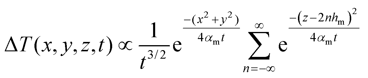 | (1) |
The temperature rise ΔT is thus obtained by multiplying the solution for a point source at the surface of an infinite 2D medium (Gaussian distribution with a width increasing as t1/2) by the solution for a point source on a 1D finite slab (Jacobi theta function). At short time scales (αmt ≪ hm2), the sum is dominated by its n = 0 term, and ΔT approximately coincides with the solution for a 3D semi-infinite substrate, with a t−3/2 dependence at the source position. Conversely, at long time scales (αmt ≫ hm2, so that the sum can be approximated by an integral),  , which corresponds to a uniform temperature along the membrane thickness and a lateral 2D diffusion of heat. The transition between the two regimes occurs for αmt ≈ hm2, i.e., for a Si3N4 membrane (αm = 5 × 10⁻⁷ m2 s−1, assuming a Λm = 1 W m−1 K−1 thermal conductivity) at times of the order of 0.5 ns and 5 ns for hm = 15 nm and hm = 50 nm, respectively. Although based on a simplified analysis, the 0.5 ns transition time for a hm = 15 nm membrane corresponds well with that at which experimental signals measured on the two membranes start to significantly deviate (Fig. 3b).
A more quantitative modeling of ND cooling dynamics necessitates to avoid the simplifications made in the previous analysis and to take into account the actual ND geometry, the non-instantaneous release of heat in the supporting membrane and the periodical character of ND optical excitation. To accomplish this, numerical simulations of the cooling dynamics of supported NDs were conducted using a previously described frequency-domain thermal model32,37 (note that an analytical treatment of the problem, such as that reported for stacked layers with infinite lateral extension,19,43 is much more challenging here because of the mixed boundary conditions at the membrane surface). This model is based on the computation, using FEM, of the frequency-dependent thermal response of a supported ND, i.e., the spatial distribution of the amplitude and phase of the temperature oscillations following a sinusoidal excitation, which summarizes the ND thermal response to any time-dependent excitation q(t).19,44 In such calculations, the amplitude of thermal oscillations decays in a frequency-dependent manner around heated regions, over a characteristic length scale given by the heat penetration length  (with Lp ≈ 40 nm in silicon nitride when f = frep = 80 MHz). This implies that for ND excitation by a train of Dirac pulses
  , which corresponds to a
  frequency content, the membrane properties (size, modalities of heat exchanges at the membrane ends and with air, which are poorly known in our experiments) at scales much larger than Lp only affect the average heating (0-frequency component). Uncertainties about the large-scale membrane properties are therefore not limiting for a quantitative analysis of the ΔT′ND(t) dynamics. Here, a Si3N4 membrane with Dm = 2 μm diameter (much smaller than the actual membrane size, thus largely reducing computational times) with fixed temperature boundary conditions (BCs) at its end and insulating BCs on its circular faces was used, as in our previous work.37D = 100 nm and h = 10 nm values were used for ND diameter and thickness. These dimensions roughly correspond to the average ones deduced from electron microscopy observations and SMS characterization on NDs from the colloidal solution used.
The fitting parameters of our model are the thermal conductance G of the Au–Si3N4 interface and the thermal conductivity Λm of Si3N4 (whose previous measurements have led to scattered results17,45–49). The ΔT′ND(t) dynamics of NDs deposited on 15 nm thick membranes can be accurately reproduced using the same values of G and Λm as in the case of 50 nm thick membranes,37 namely G = 150 MW m−2 K−1 and Λm = 1 W m−1 K−1. This is illustrated in Fig. 3b, which shows the ΔT′ND(t) dynamics computed for NDs supported on Si3N4 membranes using these G and Λm values (solid purple and orange lines). The excellent reproduction of experimental signals at <0.5 ns delays (at which ΔT′ND dynamics are mostly controlled by G and Λm![[thin space (1/6-em)]](https://www.rsc.org/images/entities/char_2009.gif) 37) using G = 150 MW m−2 K−1 and Λm = 1 W m−1 K−1 indicates that these values constitute accurate estimations of G and Λm (with uncertainties of the order of 10%) for both 50 and 15 nm thick membranes. The slight shift between the measured and modeled ΔT′ND(t) dynamics at >1 ns delays could have several causes, including a slight difference between the nominal and actual values of the membrane thickness. Regarding the ΔTND(t) dynamics (Fig. 3a), one can observe that the ΔTND(0−) temperature rises predicted by the model are higher by about 50% than the measured ones, similarly to previous observations for ≈50 nm thick membranes.37 This difference, which would increase with the use in the modeling of larger Dm values, closer to the actual membrane size, suggests that the thermal coupling of the membrane with ambient air taking place at the top and bottom planar surfaces of the membrane (not included in the modeling where dissipation only occurs at the membrane lateral ends) plays a significant role in large-scale membrane cooling.
37) using G = 150 MW m−2 K−1 and Λm = 1 W m−1 K−1 indicates that these values constitute accurate estimations of G and Λm (with uncertainties of the order of 10%) for both 50 and 15 nm thick membranes. The slight shift between the measured and modeled ΔT′ND(t) dynamics at >1 ns delays could have several causes, including a slight difference between the nominal and actual values of the membrane thickness. Regarding the ΔTND(t) dynamics (Fig. 3a), one can observe that the ΔTND(0−) temperature rises predicted by the model are higher by about 50% than the measured ones, similarly to previous observations for ≈50 nm thick membranes.37 This difference, which would increase with the use in the modeling of larger Dm values, closer to the actual membrane size, suggests that the thermal coupling of the membrane with ambient air taking place at the top and bottom planar surfaces of the membrane (not included in the modeling where dissipation only occurs at the membrane lateral ends) plays a significant role in large-scale membrane cooling.
The deduction of similar Λm values from the analysis of the ΔT′ND(t) dynamics measured on 50 nm and 15 nm thick membranes stands in stark contrast to findings on silicon membranes of similar thickness, whose thermal conductivity was seen to be strongly thickness-dependent and up to ≈5 times smaller than the bulk silicon one.28 This disparity in the thickness-dependence of the thermal properties of Si3N4 and Si membranes can be attributed to the large difference between the heat conductivity and phonon mean free paths of these two materials in the bulk form. Indeed, amorphous media such as silica and silicon nitride have a ≈1 nm room temperature phonon mean free path, while in crystalline silicon a large fraction of phonons have >100× longer mean free paths.15,22,50 Experimental observations are thus consistent with the fact that membrane thickness reduction in the tens of nm range should significantly diminish the mean free path of phonons in Si, but not in Si3N4.
The ΔTND(t) dynamics were also computed in the case of ND excitation by a single pump pulse, which corresponds to discarding accumulation effects (dashed lines in Fig. 3). These complementary calculations allow to appreciate the respectively strong and relatively weak influences of a repeated ND excitation on the ΔTND(t) and ΔT′ND(t) dynamics. They also enable a clear visualization of the transition from a 3D to a 2D heat diffusion in a membrane heated by a source located at its surface, discussed above based on analytical expressions. This transition is illustrated in Fig. 3c, which presents snapshots of the temperature profiles computed for single pulse excitation of a ND positioned on a 15 nm or 50 nm thick membrane. At t = 0.1 ns heat diffusion presents a distinct 3D character, with only regions less than 10 nm away from the ND being significantly heated. Conversely, at t = 1 ns the temperature profile has become independent of depth for a 15 nm thick membrane (but not for a 50 nm thick one). At t = 10 ns (a delay exceeding the experimentally accessible ones) diffusion has evolved into a 2D process in both cases, resulting in depth-independent temperature distributions.
2.3. Sensitivity of time-resolved signals to ND and membrane heating
The analysis of time-resolved signals measured by varying the probe wavelength λpr (Fig. 2) necessitates a more complete modeling addressing not only the cooling dynamics of membrane-supported NDs, but also the transient changes of ND extinction cross-section σext that they induce. A useful starting point for interpreting these measurements is the situation of uniform temperatures in both the ND and its local supporting membrane, noted TND and Tm.24,31 In this case, simplified as compared to the experimental one where only the ND temperature can be reasonably considered as uniform (because of the high thermal conductivity of gold), the extinction changes induced by small modifications of TND and Tm can be written as| Δσext(λpr) = AND(λpr)ΔTND + Am(λpr)ΔTm | (2) |
 | (3) |
 derivative vanishes for λpr ≈ λSPR, which explains the possibility of selectively probing ΔTND in this wavelength range.31 The temperature-dependence of gold dielectric function has been previously measured and modeled.51–57 We used here the data from ref. 53, as in our recent works.32,37εm = 4.12 and
  were used for Si3N4, consistently with previous measurements.58
As each pump pulse deposits energy in the ND only, the extinction modification immediately following ND excitation and internal thermalization is solely due to an increase of ND temperature. This enables experimental extraction of the wavelength-dependent AND coefficient appearing in eqn (2) and (3), by evaluating the variation of the thermal components of Δσext(t)/ΔT0 (Fig. 2) following ND excitation by the pump pulse. The AND spectra deduced from measurements on two NDs are plotted in Fig. 4a, as a function of λpr − λSPR to facilitate the comparison between the different measurements, as λSPR slightly varies from one ND to another and presents for some NDs a slight polarization dependence, signature of a small ND elongation.38 They are similar for the two investigated NDs and polarizations. ND heating produces a negative σext variation for λpr − λSPR < 20 nm and a positive one for higher λpr values. The maximal |AND| value, obtained for λpr ≈ λSPR, is of the order of 40 nm2 K−1. The AND spectra resemble those previously measured on lithographed NDs,32 with however different maximal |AND| values, which can be ascribed to the use of NDs with different dimensions in the two studies.
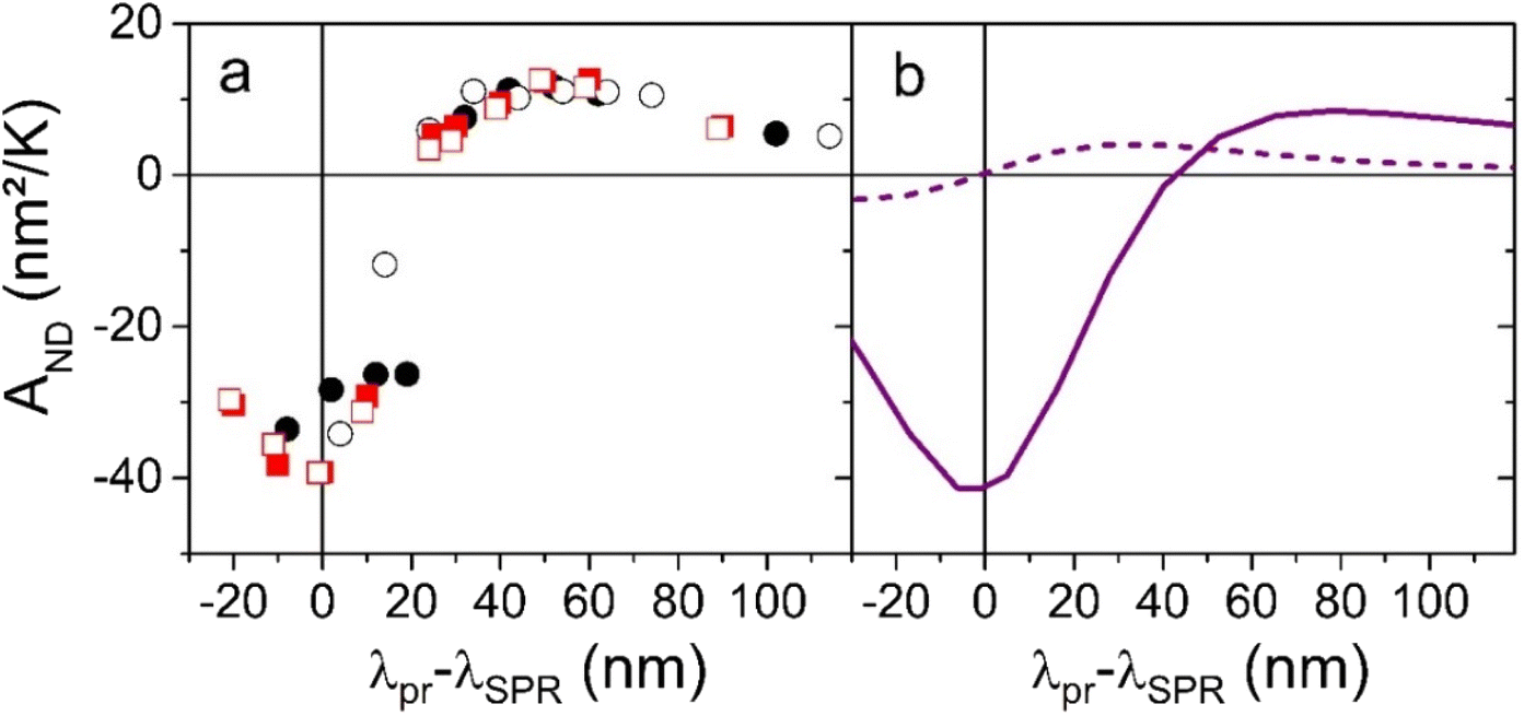 | ||
| Fig. 4 Sensitivity of ND extinction cross-section to ND heating. (a) Sensitivity deduced from time-resolved experiments (see eqn (2) and (3) for AND definition). The experimental results were obtained on two distinct NDs (black circles and red squares) for two orthogonal polarizations of the probe beam (solid and hollow symbols). (b) Sensitivity computed using FEM optical simulations and temperature dependence of gold dielectric function from ref. 53 (solid purple line). The computed sensitivity to Si3N4 membrane heating is also shown for comparison (dashed line). | ||
Due to the large uncertainties on the temperature dependence of gold dielectric function (eqn (3)), whose measurement has led to scattered results,51–57 obtaining a precise match between the measured and modeled AND spectra is hardly achievable. Nevertheless, the AND spectrum computed based on eqn (3), shown in Fig. 4b, presents spectral variations and absolute values similar to the measured ones, mostly differing by the spectral position of the AND sign change, which is located further away from λSPR in the simulation case. The general shape of the AND spectrum results from the much larger temperature-dependence of ε2 (which mostly influences SPR width) as compared to ε1 (which mostly impacts SPR position) in eqn (3). ND heating thus mostly induces a broadening of SPR, leading to a decrease of σext close to λSPR and to an increase further away from λSPR. The computed Am spectrum is also shown in Fig. 4b. Its spectral shape largely differs from the AND one, which is due to the fact that membrane heating mostly affects SPR position. |Am| is usually much smaller than |AND| (Fig. 4b). However, this is not the case in the ≈20 nm broad spectral range around the wavelength where AND vanishes, suggesting that measurements with λpr in this spectral range should be very significantly affected by membrane heating.
Fig. 5a shows the Δσext,norm(t) dynamics measured for different λpr values (obtained by dividing Δσext(t) by its initial value) do not overlap. As λpr is increased on the red flank of the resonance, the Δσext,norm(t) dynamics become initially slightly faster (λpr − λSPR = 10 nm) and then much slower (λpr − λSPR = 25–30 nm). A complementary illustration of the λpr-dependence of the Δσext,norm(t) is shown in Fig. 5b, where the Δσext,norm value at the maximal pump–probe delay (2.7 ns) is plotted as a function of λpr. While 0.15 values are observed for most λpr values, significantly larger values, up to 0.45 (corresponding to much slower dynamics) are observed for λpr − λSPR = 20–30 nm. This λpr-dependence of the Δσext,norm(t) dynamics indicates that the transient ND optical response is not simply proportional to ΔTND(t) when λpr ≠ λSPR, especially when the sensitivity to ND heating is small and changes sign (λpr − λSPR = 20–30 nm, Fig. 4a), and strongly suggests that Δσext is significantly affected by environment heating.
 | ||
| Fig. 5 Influence of Si3N4 membrane heating on the dynamics of transient ND extinction changes. (a) Examples of normalized thermal components of Δσext measured on a single ND using different λpr values. (b) Average value of the normalized extinction change measured at 2.7 ns pump–probe delay (maximal delay in the experiments) for different NDs and polarizations. The same color code as in Fig. 4 was used. (c) Examples of normalized Δσext changes FEM-computed using different λpr values. (d) Normalized extinction change after 3 ns computed using FEM. | ||
Comparison of the measured signals with the predictions of a complete thermo-optical model taking into account the inhomogeneous and time-dependent temperature rise inside the membrane is useful to fully demonstrate this hypothesis. The Δσext(t) dynamics were thus simulated using the two-step modeling procedure discussed in ref. 31. It basically consists in complementing the purely thermal FEM computations discussed above, which provide the spatially- and time-dependent temperature rise profiles in the ND and the membrane, with optical FEM simulations estimating the temporal evolution of the ND extinction cross-section σext. To do so, σext was recalculated at various delays using dielectric functions modified in a spatially-dependent way, as (considering the example of the membrane one)  . The predictions of the model regarding the Δσext,norm(t) dynamics and its value after 3 ns are shown in Fig. 5c and d. The trends observable in these plots are very close to those of the experimental results, shown in Fig. 5a and b. In particular, the modeled results also feature a considerable slow-down of the dynamics (associated with a much larger final Δσext,norm value) for probe wavelengths slightly higher than that at which AND vanishes. Additionally, the model also predicts much faster dynamics at slightly lower wavelength, an effect which could not be observed experimentally (essentially because the raw signals measured in this range are difficult to analyze, as they present strong oscillations and low-amplitude thermal components).
3. Conclusion
The thermo-optical dynamics of gold NDs supported on a nanometric Si3N4 membrane were investigated both experimentally and numerically in this work. Decrease of the membrane thickness from 50 nm to 15 nm was seen to considerably slow down the ND cooling dynamics, and to increase its average heating for periodical pulsed excitation. This effect can be ascribed to the evolution of heat diffusion in the membrane from a 3D process to a 2D one after about 0.5 ns, the time required for heat to propagate over 15 nm in Si3N4. The significant heating of the membrane induced by its small thickness and the high (for a solid material) temperature-dependence of the Si3N4 refractive index also allowed us to demonstrate the dependence of the ND transient optical response on probe wavelength. Strong variations of the time dependence of this transient response were in particular observed in the narrow wavelength range where environment contribution becomes of the order of (or even larger than) the ND heating contribution. These results could be useful for applications requiring to minimize the cooling kinetics of nanostructures or for local probing of temperature or thermal properties of thin membranes using metal nanoparticles as thermometers. The extension of this work to situations involving nanoparticle size and/or membrane thickness smaller than phonon mean free paths in the membrane may also improve the fundamental understanding of nanoscale heat transport.4. Methods
4.1. ND synthesis and deposition
The synthesis of Gold NDs was performed in aqueous solution in presence of the cetyltrimethylammonium bromide (CTAB) surfactant, following an already published protocol.37,59 Gold nanoplates were first synthesized by adapting a protocol initially used to produce triangular nanoplates,60 using modified concentrations of the reactants in the growth solution (CTAB 0.1 M, HAuCl4 0.7 mM and ascorbic acid 1.6 mM), yielding nanoplates with ≈90% hexagonal and ≈10% triangular sections. Au NDs were subsequently obtained by smoothing the vertices and edges of the nanoplates through mild oxidation using the Au(III)/CTAB oxidant complex, as detailed elsewhere.61,62 Deposition of the NDs for single-particle optical investigations was performed on a 15 nm thick silicon nitride (Si3N4) membrane patterned into 100 × 100 μm apertures, etched in a 200 nm thick support mesh (Ted Pella). The immobilization of NDs on these substrates was conducted by depositing a drop of highly diluted gold ND solution which was subsequently left to dry, leading to a low density of deposited NDs (<1 ND per μm2), as required for far-field single-particle optical studies. Multiple thorough ethanol rinses followed by a UV/ozone treatment were administered to minimize the presence of organic residues.634.2. ND optical detection and characterization
The localization and extinction spectroscopy of individual NDs were conducted using spatial modulation spectroscopy (SMS). This far-field microscopy/spectroscopy optical technique relies on the periodic displacement of a sample illuminated by a tightly focused light beam, which induces a modulation of the transmitted light power when a nano-object is present in the light beam.33,64 SMS was initially employed to locate single NDs following their random deposition on the Si3N4 membrane and, subsequently, for measuring their absolute extinction cross-section σext as a function of the illumination wavelength λ and light polarization angle θ. SMS experiments were performed using a light source spanning the 375–1040 nm wavelength range, obtained by combining a tunable femtosecond Ti:sapphire oscillator (emitting λ = 690–1040 nm pulses at a repetition frequency of frep = 80 MHz) with a visible optical parametric oscillator and a frequency-doubling BBO crystal. The light beam delivered by this source was focused on the sample by a 100× microscope objective, resulting in nearly diffraction-limited spot sizes with a full-width at half-maximum of approximately 0.7λ. Control over the direction of the beam linear polarization was achieved using a wire grid polarizer. Spatial modulation of the sample was performed at f = 1.5 kHz frequency with 300 nm modulation amplitude and lock-in detection at 2f.4.3. Time-resolved experiments
The transient optical response of individual NDs was measured using single-particle femtosecond pump–probe spectroscopy,36,65 an approach based on the illumination of the investigated nanoparticle, previously detected by SMS, with two spatially overlapping, tightly focused and time-delayed femtosecond pump and probe light pulses. Time-resolved measurements on individual NDs were performed by combining the SMS microscope with a two-color pump–probe setup based on the femtosecond laser source described above, delivering ∼150 fs pulses. The oscillator pulse train was split in two parts to generate the pump and probe beams. The pump beam was produced using second harmonic generation (yielding λpp in the 375–510 nm range), whereas the probe beam was either the signal from the Ti:sapphire oscillator (with λpr = 750–1020 nm in this case) or the output of the optical parametric oscillator (λpr = 500–730 nm, with λpp = 410 nm). To improve signal to noise ratio, a mechanical chopper operating at 30 kHz was used for pump power modulation. The pump-induced relative changes of the probe beam transmission, ΔTr/Tr, were then measured using synchronous detection as a function of the time interval separating the pump and probe pulses, controlled by a mechanical delay line. This raw measured signal is directly related to the transient changes of the extinction cross-section σext(λpr) of the investigated nano-object at probe wavelength λprvia ΔTr/Tr = −Δσext(λpr)/Spr, with Spr = πdfwhm2/(4ln2) representing the area of the probe spot (which can be estimated by analysis of SMS images) and dfwhm its full-width at half-maximum.65
4.4. Thermal simulations
Modeling of the ND linear optical response, cooling dynamics and transient optical response was performed using a finite-element modeling (FEM) commercial software. In all these simulations, Gold NDs were described as circular cylinders characterized by their thickness h and diameter D, and the 15 nm thick Si3N4 membrane supporting them was explicitly included. Thermal simulations were done considering a cylindrical membrane with a Dm = 2 μm diameter, with thermal insulation boundary conditions on its upper and lower circular bases, and constant temperature ones on its lateral surface. 2D axisymmetric simulations exploiting the rotational symmetry of the considered geometry were performed, allowing to greatly reduce the required computational times. 2.49 and 2.13 MJ m−3 K−1 values were used for the specific heats of Au and Si3N4. A 317 W m−1 K−1 value (bulk gold value) was used for the ND thermal conductivity. The heat conductivity of Si3N4 and the thermal conductance at the Au–Si3N4 interface were left as free parameters. FEM was used to compute the frequency-domain response![[h with combining tilde]](https://www.rsc.org/images/entities/i_char_0068_0303.gif) (f) of a supported gold ND, i.e. the frequency- and position-dependent amplitudes and phases of the temperature oscillations following sinusoidal energy injection in the ND. The Fourier transform
(f) of a supported gold ND, i.e. the frequency- and position-dependent amplitudes and phases of the temperature oscillations following sinusoidal energy injection in the ND. The Fourier transform  of the thermal dynamics induced by any time-dependent excitation process q(t), of Fourier transform
 ![[q with combining tilde]](https://www.rsc.org/images/entities/i_char_0071_0303.gif) (f), can then be deduced from (f) by computing
(f), can then be deduced from (f) by computing  , allowing to deduce the corresponding temporal dynamics ΔT(t) by reverse Fourier transform.37
4.5. Optical and thermo-optical simulations
A simulation domain containing the ND and the Si3N4 membrane with air above and below it, surrounded by a perfectly matched layer was considered for computing the optical response of gold NDs. Refractive indexes of 2.03 and 1 were used for Si3N4 and air, respectively. The dielectric function ε = ε1 + iε2 of bulk gold in the visible/near-infrared range can be written as the sum of interband (ib) and intraband (Drude-like) components as33,66,67 , with ωp the plasma frequency and γ the optical scattering rate of the conduction electrons (ħωp = 9.01 eV and ħγ ≈ 50 meV for bulk gold). In this work, we used bulk ωp and εib values (the latter being deduced from Johnson and Christy tables68) and ħγ values larger (typically by ≈100 meV) than the bulk gold value, as required to reproduce the SPR widths measured on single nano-objects. This corresponds to taking into account additional non-radiative plasmon damping mechanisms in metal nano-objects as compared to the bulk metal case.69–72 ND illumination by a linearly polarized plane wave was considered. Absorption and scattering cross-sections were deduced from the computed electric field profiles, and summed to yield the extinction one σext. The ∂σext/∂ε1 and ∂σext/∂ε2 partial derivatives were deduced from these calculations by computing σext with slightly modified ε1 or ε2 values and then performing discrete derivation.
The transient optical response of NDs induced by their thermal dynamics was computed by reproducing the previous calculations at various stages of the thermal dynamics, using non-uniform dielectric functions locally modified as compared to room-temperature Au and Si3N4 values as 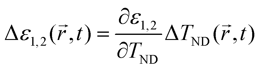 and
and 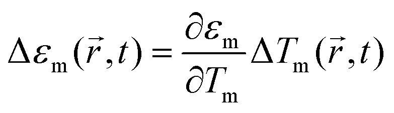 .
.  was used for Si3N4, while wavelength-dependent tables from ref. 53 were used for
  .
.
Conflicts of interest
There are no conflicts to declare.Acknowledgements
This work was supported by the French National Research Agency (ANR) under the reference ANR-20-CE30-0016 (ULTRASINGLE project).References
- D. G. Cahill, W. K. Ford, K. E. Goodson, G. D. Mahan, A. Majumdar, H. J. Maris, R. Merlin and S. R. Phillpot, J. Appl. Phys., 2003, 93, 793–818 CrossRef CAS.
- D. G. Cahill, P. V. Braun, G. Chen, D. R. Clarke, S. Fan, K. E. Goodson, P. Keblinski, W. P. King, G. D. Mahan, A. Majumdar, H. J. Maris, S. R. Phillpot, E. Pop and L. Shi, Appl. Phys. Rev., 2014, 1, 011305 Search PubMed.
- E. Pop, S. Sinha and K. E. Goodson, Proc. IEEE, 2006, 94, 1587–1601 CAS.
- G. J. Snyder and E. S. Toberer, Nat. Mater., 2008, 7, 105–114 CrossRef CAS PubMed.
- G. Baffou, F. Cichos and R. Quidant, Nat. Mater., 2020, 19, 946–958 CrossRef CAS PubMed.
- E. T. Swartz and R. O. Pohl, Appl. Phys. Lett., 1987, 51, 2200–2202 CrossRef CAS.
- E. Swartz and R. Pohl, Rev. Mod. Phys., 1989, 61, 605–668 CrossRef.
- G. Chen, J. Heat Transfer, 1996, 118, 539–545 CrossRef CAS.
- M. E. Siemens, Q. Li, R. Yang, K. A. Nelson, E. H. Anderson, M. M. Murnane and H. C. Kapteyn, Nat. Mater., 2010, 9, 26–30 CrossRef CAS PubMed.
- A. J. Minnich, J. A. Johnson, A. J. Schmidt, K. Esfarjani, M. S. Dresselhaus, K. A. Nelson and G. Chen, Phys. Rev. Lett., 2011, 107, 095901 CrossRef CAS PubMed.
- Y. K. Koh and D. G. Cahill, Phys. Rev. B: Condens. Matter Mater. Phy, 2007, 76, 1–5 Search PubMed.
- R. B. Wilson and D. G. Cahill, Nat. Commun., 2014, 5, 1–11 Search PubMed.
- A. J. Schmidt, R. Cheaito and M. Chiesa, Rev. Sci. Instrum., 2009, 80, 094901 CrossRef PubMed.
- K. T. Regner, D. P. Sellan, Z. Su, C. H. Amon, A. J. H. McGaughey and J. A. Malen, Nat. Commun., 2013, 4, 1640 CrossRef PubMed.
- S. Dilhaire, G. Pernot, G. Calbris, J. M. Rampnoux and S. Grauby, J. Appl. Phys., 2011, 110, 114314 CrossRef.
- S. Grauby, B. Vidal Montes, A. Zenji, J.-M. Rampnoux and S. Dilhaire, ACS Photonics, 2022, 9, 3734–3744 CrossRef CAS.
- S.-M. Lee and D. G. Cahill, J. Appl. Phys., 1997, 81, 2590–2595 CrossRef CAS.
- M. Hu, X. Wang, G. V. Hartland, V. Salgueiriño-Maceira and L. M. Liz-Marzán, Chem. Phys. Lett., 2003, 372, 767–772 CrossRef CAS.
- D. G. Cahill, Rev. Sci. Instrum., 2004, 75, 5119–5122 CrossRef CAS.
- Z. Ge, D. G. Cahill and P. V. Braun, J. Phys. Chem. B, 2004, 108, 18870–18875 CrossRef CAS.
- V. Juvé, M. Scardamaglia, P. Maioli, A. Crut, S. Merabia, L. Joly, N. Del Fatti and F. Vallée, Phys. Rev. B: Condens. Matter Mater. Phy, 2009, 80, 195406 CrossRef.
- J. A. Johnson, A. A. Maznev, J. Cuffe, J. K. Eliason, A. J. Minnich, T. Kehoe, C. M. S. Torres, G. Chen and K. A. Nelson, Phys. Rev. Lett., 2013, 110, 025901 CrossRef PubMed.
- J. Huang, J. Park, W. Wang, C. J. Murphy and D. G. Cahill, ACS Nano, 2013, 7, 589–597 CrossRef CAS PubMed.
- T. Stoll, P. Maioli, A. Crut, S. Rodal-Cedeira, I. Pastoriza-Santos, F. Vallée and N. Del Fatti, J. Phys. Chem. C, 2015, 119, 12757–12764 CrossRef CAS.
- L. Zeng, K. C. Collins, Y. Hu, M. N. Luckyanova, A. A. Maznev, S. Huberman, V. Chiloyan, J. Zhou, X. Huang, K. A. Nelson and G. Chen, Sci. Rep., 2015, 5, 1–10 Search PubMed.
- M. Tamura, T. Iida and K. Setoura, Nanoscale, 2022, 14, 12589–12594 RSC.
- E. Chávez-Ángel, J. S. Reparaz, J. Gomis-Bresco, M. R. Wagner, J. Cuffe, B. Graczykowski, A. Shchepetov, H. Jiang, M. Prunnila, J. Ahopelto, F. Alzina and C. M. Sotomayor Torres, APL Mater., 2014, 2, 012113 CrossRef.
- J. Cuffe, J. K. Eliason, A. A. Maznev, K. C. Collins, J. A. Johnson, A. Shchepetov, M. Prunnila, J. Ahopelto, C. M. Sotomayor Torres, G. Chen and K. A. Nelson, Phys. Rev. B: Condens. Matter Mater. Phy, 2015, 91, 245423 CrossRef.
- D. Li, Y. Wu, P. Kim, L. Shi, P. Yang and A. Majumdar, Appl. Phys. Lett., 2003, 83, 2934–2936 CrossRef CAS.
- Y. S. Ju and K. E. Goodson, Appl. Phys. Lett., 1999, 74, 3005–3007 CrossRef CAS.
- M. Gandolfi, A. Crut, F. Medeghini, T. Stoll, P. Maioli, F. Vallée, F. Banfi and N. Del Fatti, J. Phys. Chem. C, 2018, 122, 8655–8666 CrossRef CAS.
- R. Rouxel, M. Diego, F. Medeghini, P. Maioli, F. Rossella, F. Vallée, F. Banfi, A. Crut and N. Del Fatti, J. Phys. Chem. C, 2020, 124, 15625–15633 CrossRef CAS.
- A. Crut, P. Maioli, N. Del Fatti and F. Vallée, Chem. Soc. Rev., 2014, 43, 3921–3956 RSC.
- R. Rouxel, M. Diego, P. Maioli, N. Lascoux, F. Vialla, F. Rossella, F. Banfi, F. Vallée, N. Del Fatti and A. Crut, J. Phys. Chem. C, 2021, 125, 23275–23286 CrossRef CAS.
- A. Crut, P. Maioli, N. Del Fatti and F. Vallée, Phys. Rep., 2015, 549, 1–43 CrossRef CAS.
- O. L. Muskens, N. Del Fatti and F. Vallée, Nano Lett., 2006, 6, 552–556 CrossRef CAS PubMed.
- C. Panais, R. Rouxel, N. Lascoux, S. Marguet, P. Maioli, F. Banfi, F. Vallée, N. Del Fatti and A. Crut, J. Phys. Chem. Lett., 2023, 14, 5343–5352 CrossRef CAS PubMed.
- F. Medeghini, R. Rouxel, A. Crut, P. Maioli, F. Rossella, F. Banfi, F. Vallée and N. Del Fatti, J. Phys. Chem. Lett., 2019, 10, 5372–5380 CrossRef CAS PubMed.
- G. V. Hartland, Chem. Rev., 2011, 111, 3858–3887 CrossRef CAS PubMed.
- F. Medeghini, A. Crut, M. Gandolfi, F. Rossella, P. Maioli, F. Vallée, F. Banfi and N. Del Fatti, Nano Lett., 2018, 18, 5159–5166 CrossRef CAS PubMed.
- H. S. Carslaw and J. C. Jaeger, Conduction of Heat in Solids, Oxford, Clarendon, 1959 Search PubMed.
- A. Tadeu and N. Simões, Eng. Anal. Bound. Elem., 2006, 30, 338–349 CrossRef.
- C. Frétigny, J.-Y. Duquesne and D. Fournier, Int. J. Thermophys., 2015, 36, 1281–1288 CrossRef.
- K. C. Collins, A. A. Maznev, J. Cuffe, K. A. Nelson and G. Chen, Rev. Sci. Instrum., 2014, 85, 124903 CrossRef PubMed.
- X. Zhang and C. P. Grigoropoulos, Rev. Sci. Instrum., 1995, 66, 1115–1120 CrossRef CAS.
- L. La Spina, A. W. van Herwaarden, H. Schellevis, W. H. A. Wien, N. Nenadovic and L. K. Nanver, J. Microelectromech. Syst., 2007, 16, 675–683 Search PubMed.
- M. T. Alam, M. P. Manoharan, M. A. Haque, C. Muratore and A. Voevodin, J. Micromech. Microeng., 2012, 22, 045001 CrossRef.
- M. Bogner, A. Hofer, G. Benstetter, H. Gruber and R. Y. Q. Fu, Thin Solid Films, 2015, 591, 267–270 CrossRef CAS.
- H. Ftouni, C. Blanc, D. Tainoff, A. D. Fefferman, M. Defoort, K. J. Lulla, J. Richard, E. Collin and O. Bourgeois, Phys. Rev. B: Condens. Matter Mater. Phy, 2015, 92, 1–7 Search PubMed.
- R. M. Costescu, M. A. Wall and D. G. Cahill, Phys. Rev. B: Condens. Matter Mater. Phy, 2003, 67, 054302 CrossRef.
- R. B. Wilson, B. A. Apgar, L. W. Martin and D. G. Cahill, Opt. Express, 2012, 20, 28829–28838 CrossRef CAS PubMed.
- Y. J. Chen, M. C. Lee and C. M. Wang, Jpn. J. Appl. Phys., 2014, 53, 08MG02 CrossRef CAS.
- T. Stoll, P. Maioli, A. Crut, N. Del Fatti and F. Vallée, Eur. Phys. J. B, 2014, 87, 260 CrossRef.
- P.-T. Shen, Y. Sivan, C.-W. Lin, H.-L. Liu, C.-W. Chang and S.-W. Chu, Opt. Express, 2016, 24, 19254 CrossRef CAS PubMed.
- H. Reddy, U. Guler, A. V. Kildishev, A. Boltasseva and V. M. Shalaev, Opt. Mater. Express, 2016, 6, 2776 CrossRef CAS.
- S. Zhang, Y. Pei and L. Liu, J. Appl. Phys., 2018, 124, 165301 CrossRef.
- M. Magnozzi, M. Ferrera, L. Mattera, M. Canepa and F. Bisio, Nanoscale, 2019, 11, 1140–1146 RSC.
- A. W. Elshaari, I. E. Zadeh, K. D. Jons and V. Zwiller, IEEE Photonics J., 2016, 8, 1–9 Search PubMed.
- S. Mitiche, S. Marguet, F. Charra and L. Douillard, Nano Res., 2020, 13, 1597–1603 CrossRef CAS.
- K. L. Young, M. R. Jones, J. Zhang, R. J. Macfarlane, R. Esquivel-Sirvent, R. J. Nap, J. Wu, G. C. Schatz, B. Lee and C. A. Mirkin, Proc. Natl. Acad. Sci. U. S. A., 2012, 109, 2240–2245 CrossRef CAS PubMed.
- J. Rodríguez-Fernández, J. Pérez-Juste, P. Mulvaney and L. M. Liz-Marzán, J. Phys. Chem. B, 2005, 109, 14257–14261 CrossRef PubMed.
- M. N. O'Brien, M. R. Jones, K. L. Kohlstedt, G. C. Schatz and C. A. Mirkin, Nano Lett., 2015, 15, 1012–1017 CrossRef PubMed.
- A. Movsesyan, S. Marguet, A. Muravitskaya, J. Béal, P.-M. Adam and A.-L. Baudrion, J. Opt. Soc. Am. A, 2019, 36, C78–C84 CrossRef CAS PubMed.
- A. Arbouet, D. Christofilos, N. Del Fatti, F. Vallée, J. Huntzinger, L. Arnaud, P. Billaud and M. Broyer, Phys. Rev. Lett., 2004, 93, 127401 CrossRef CAS PubMed.
- H. Baida, D. Mongin, D. Christofilos, G. Bachelier, A. Crut, P. Maioli, N. Del Fatti and F. Vallée, Phys. Rev. Lett., 2011, 107, 057402 CrossRef CAS PubMed.
- U. Kreibig and M. Vollmer, Optical Properties of Metal Clusters, Springer, New York, 1995 Search PubMed.
- H. Hövel, S. Fritz, A. Hilger, U. Kreibig and M. Vollmer, Phys. Rev. B: Solid State, 1993, 48, 18178–18188 CrossRef PubMed.
- P. B. Johnson and R. W. Christy, Phys. Rev. B: Solid State, 1972, 6, 4370–4379 CrossRef CAS.
- H. Baida, P. Billaud, S. Marhaba, D. Christofilos, E. Cottancin, A. Crut, J. Lermé, P. Maioli, M. Pellarin, M. Broyer, N. Del Fatti, F. Vallée, A. Sánchez-Iglesias, I. Pastoriza-Santos and L. M. Liz-Marzán, Nano Lett., 2009, 9, 3463–3469 CrossRef CAS PubMed.
- V. Juvé, M. F. Cardinal, A. Lombardi, A. Crut, P. Maioli, J. Pérez-Juste, L. M. Liz-Marzán, N. Del Fatti and F. Vallée, Nano Lett., 2013, 13, 2234–2240 CrossRef PubMed.
- P. Zijlstra, P. M. R. Paulo, K. Yu, Q.-H. Xu and M. Orrit, Angew. Chem., Int. Ed., 2012, 51, 8352–8355 CrossRef CAS PubMed.
- B. Foerster, V. A. Spata, E. A. Carter, C. Sönnichsen and S. Link, Sci. Adv., 2019, 5, eaav0704 CrossRef CAS PubMed.
| This journal is © The Royal Society of Chemistry 2024 |