
Effective surface passivation of GaAs nanowire photodetectors by a thin ZnO capping
Fuxiang
Shang
 a,
Chaofei
Zha
b,
Hanchen
Zhu
a,
Zheyu
Zhang
a,
Yuanhao
Shen
c,
Qichao
Hou
a,
Linjun
Zhang
a,
Yanmeng
Chu
a,
Lulu
Chen
a,
Junjie
Zhao
c,
Wenzhang
Fang
a,
Yishu
Zhang
a,
Zhiyuan
Cheng
*a and
Yunyan
Zhang
*a
a,
Chaofei
Zha
b,
Hanchen
Zhu
a,
Zheyu
Zhang
a,
Yuanhao
Shen
c,
Qichao
Hou
a,
Linjun
Zhang
a,
Yanmeng
Chu
a,
Lulu
Chen
a,
Junjie
Zhao
c,
Wenzhang
Fang
a,
Yishu
Zhang
a,
Zhiyuan
Cheng
*a and
Yunyan
Zhang
*a
aCollege of Integrated Circuits, Zhejiang University, Hangzhou, Zhejiang 311200, China. E-mail: yunyanzhang@zju.edu.cn
bState Key Laboratory of Information Photonics and Optical Communications, Beijing University of Posts and Telecommunications, Beijing 100876, China
cState Key Laboratory of Chemical Engineering, College of Chemical and Biological Engineering, Zhejiang University, 866 Yuhangtang Rd, Hangzhou 310027, China
First published on 4th June 2024
Abstract
The III–V nanowire (NW) structure is a good candidate for developing photodetectors. However, high-density surface states caused by the large surface-to-volume ratio severely limit their performance, which is difficult to solve in conventional ways. Here, a robust surface passivation method, using a thin layer of ZnO capping, is developed for promoting NW photodetector performance. 11 cycles of ZnO, grown on pure zinc blende high-quality GaAs NWs by atomic layer deposition, significantly alleviates the undesirable effect of the surface states, without noticeable degradation in NW morphology. An average 20-fold increase in micro-photoluminescence intensity is observed for passivated NWs, which leads to the development of detectors with high responsivity, specific detectivity, and optical gain of 9.46 × 10⁵ A W−1, 3.93 × 10¹⁴ Jones, and 2.2 × 10⁸ %, respectively, under low-intensity 532 nm illumination. Passivated NW detectors outperform their counterparts treated by conventional methods, so far as we know, which shows the potential and effectiveness of thin ZnO surface passivation on NW devices.
 Yunyan Zhang | Yunyan Zhang received his Ph.D. from University College London (UCL) within three years and was appointed as a Research Associate in UCL. Thereafter, he moved to Germany as a senior lecturer at Paderborn University. He is currently a professor in Zhejiang University. He is devoted to the deep understanding of nanowire growth mechanisms including nucleation, doping, and uniformity. His research interest focuses on high-quality material growth and device fabrication for III–V semiconductor nanowire microelectronics and optoelectronics. |
1. Introduction
Photodetectors based on semiconductor nanowires (NWs) with a quasi-one-dimensional morphology have received immense attention over recent years, owing to their dislocation-free growth on foreign substrates, strong light–matter interaction, and excellent light-trapping effect.1–3 The possibility of high quantum efficiency and photoresponsivity motivates future research on nanowire photodetectors. Numerous methods are demonstrated to boost nanowire photodetector behavior, including doping,4 passivation,5 surface plasmon,6 improvement in material quality,7 and more complex configurations.8,9 It is worth noting that III–V nanostructures attract widespread attention, because of their wide tunable bandgaps, high integration potential, and high absorption efficiency.10,11However, the large surface-to-volume ratio of NWs relative to the thin-film structure causes a high density of the surface states that could act as efficient recombination and scattering centers for carriers. The majority of III–V materials suffer from a large surface recombination velocity due to the surface states, such as that for GaAs, which is estimated to be the order of 106 cm s−1,12 which significantly impedes the development and optimization of optoelectrical devices. In particular, for small-diameter nanowires, the conductivity could even be switched off due to complete depletion by surface band bending,13 rendering them unsuitable for some devices.
Passivation is thus needed to produce a stable inert film to saturate dangling bonds and prevent surface oxidation. In general, common cost-effective surface passivation for III–V materials includes dielectric atomic layer deposition (ALD),14–16 sulfur treatment,17 nitridation,18 a sol–gel SiO2 shell,19 annealing, acid, and plasma treatment.20 However, chemical surface treatment, such as sulfur passivation, is not a preferable choice for long-term passivation as its effect could vanish easily under an ambient atmospheric environment.21 The plasma treatment energy needs to be carefully optimized to achieve less roughness, due to ion bombardment. Although nitridation could guarantee surface state suppression for a time, the use of toxic and dangerous reagents is an important issue.
As an extensively researched wide bandgap semiconductor material, zinc oxide (ZnO) is focused on because of its properties of long-term stability, optical transparency, passivation effect, carrier-selective transport, and high electron mobility.22 Some efforts have been made to combine ZnO and III–V materials for behavioral improvement, in fabricating high-performance MOSFETs, solar cells, photodetectors, or capacitors.23–26 Nevertheless, the potential for modifying photodetectors based on III–V NWs has still not been fully explored up to date. Although there exist some reports based on a combination of III–V NWs and ZnO,27–30 they commonly use thick n-type ZnO shells, which are unable to extract the sole role of passivation because of the formation of a possible strong pn junction and strain defects due to lattice mismatch. The use of an ultrathin oxide passivation layer can effectively solve all these side effects brought about by a thick passivation layer, as the thin thickness is not enough to accumulate a large enough strain to change the sample morphology or band bending. Previous reports have claimed that an ultrathin ZnO layer is sufficient for passivation.26,31,32 However, an ultrathin oxide passivation layer has rarely been used on NW structures, especially for photodetector fabrication. Our work demonstrates that this ultrathin ZnO layer strategy by atomic layer deposition is a promising passivation method for the nanowires without causing degradation in material quality.
GaAs (with a moderate direct bandgap of 1.42 eV) is a valuable and competitive candidate for optical detecting functions as it shows good ability for light absorption and light conversion due to its direct bandgap. Previously, we have grown high-quality phase-pure GaAs NWs by a self-catalyzed method, which could avoid generating deep trap levels by incorporation of foreign catalyst impurities and have developed optical detectors, demonstrating outstanding responsivity and specific detectivity.33 Based on that work, an efficient passivation scheme is explored for further improvements.
In this report, the development of NW surface treatment is continued using pure zinc blende (ZB) high-quality GaAs NWs that can prevent the side effects of stacking faults, such as carrier scattering and transportation barriers. A thin ZnO surface passivation layer of only 11 cycles is grown conformally by atomic layer deposition (ALD) on NWs to achieve persistent protection and avoid the side effect of using a thick layer. The effective passivation of thin ZnO on these GaAs NWs is shown by optical properties and Schottky-type photodetector performance.
2. Experimental methods
GaAs nanowire growth and characterization
GaAs NWs are grown by a self-catalyzed method on p-type Si substrates via solid-source molecular beam epitaxy (MBE) with nominal p-doping (beryllium) in the order of 1018 cm−3. These nanowires have a pure ZB crystal structure up to the top-most bilayer, which is optional for developing superior photodetectors owing to the absence of scattering centers and carrier-transportation barriers caused by stacking faults. The nanowires used in this study come from the same sample as in our previous publication, where TEM images and electron diffraction patterns show a pure ZB crystal structure.33 The average length and diameter of doped GaAs nanowires are measured to be 4 μm and 60 nm, respectively. For undoped GaAs nanowires, the average length and diameter are 10 μm and 180 nm, respectively.The micro-photoluminescence (μ-PL) intensity spectra of at least 12 individual intrinsic GaAs nanowires were measured at room temperature with a 532 nm excitation laser. The laser spot size was about 1 μm in diameter, focused by an objective lens. The morphology of the fabricated device was observed by scanning electron microscope (SEM). The chemical states of ZnO were investigated via X-ray photoelectron spectroscopy (XPS).
Device fabrication and measurements
To fabricate a single GaAs nanowire-based photodetector, a heavily p-doped silicon substrate with thermally grown 100 nm SiO2 was utilized. As-grown GaAs nanowires were transferred onto an SiO2/Si substrate by ultrasonic treatment in isopropyl alcohol (IPA) solution and subsequent drop-casting. The GaAs nanowires were immersed in dilute hydrochloric acid (HCl) for about 60 seconds to remove their native oxide. Afterward, ZnO thin films were grown at 120 degrees by thermal ALD, which is superior for damage-free and conformal deposition. Diethylzinc (DEZn) and deionized water were used as precursors to grow the ZnO thin films with a nominal growth rate of 0.17 nm per cycle. 11 cycles were used for the growth of each passivation layer. The ZnO shell thickness was around 2 nm, which was characterized by the growth of ZnO on dummy Si substrates. The positions of the nanowires were mapped with a microscope, and then, electrical contacts on both ends of the nanowires were patterned by HEIDELBERG DWL66+ maskless photolithography. After that, ZnO at the contact area was removed, followed by deposition of Cr/Au (20/80 nm) electrodes. After a lift-off process in acetone, the electrical and optoelectric responses of GaA nanowire devices were characterized using a semiconductor parameter analyzer. A light power meter was used to measure the illumination intensity.3. Results and discussion
During the initial stage of ZnO growth by ALD, the deposition rate per cycle could be less than a monolayer. The growth mode could be attributed to the induction time for the nucleation of ZnO nuclei on a foreign substrate.34 Furthermore, in situ X-ray fluorescence data for ZnO ALD grown on an InGaAs substrate verified that Zn desorption from the substrate surface should be responsible for the extremely slow growth rate (<0.05 nm per cycle) during the first several cycles.35 Consequently, the ALD-ZnO process on the GaAs nanowires for only a few cycles is considered to be a surface treatment instead of a physically complete and distinct layer.The μ-PL intensity of intrinsic GaAs NWs could indicate the relative density of the surface states, because the increase in PL intensity is related to the lower recombination velocity. The intrinsic GaAs nanowires could behave as weakly p-doped semiconductors, because of native acceptor defects, such as Ga vacancies. To avoid PL signal interference from the silicon substrate, individual nanowires were transferred onto the quartz flake. PL spectra were measured under an excitation laser with 532 nm wavelength at room temperature. As shown in Fig. 1, an average 20-fold increase in the peak intensity for the individual nanowires passivated by ALD was obtained, indicating a significant reduction in surface recombination velocity. Considerable passivation results are within expectations, because nearly complete Fermi level depinning from the valence band edge can be achieved for p-GaAs passivated by ALD ZnO.31 A higher doping level could cause a thinner surface depletion area; hence the effect of the surface states is more severe for the intrinsic GaAs nanowires than that for doped ones.
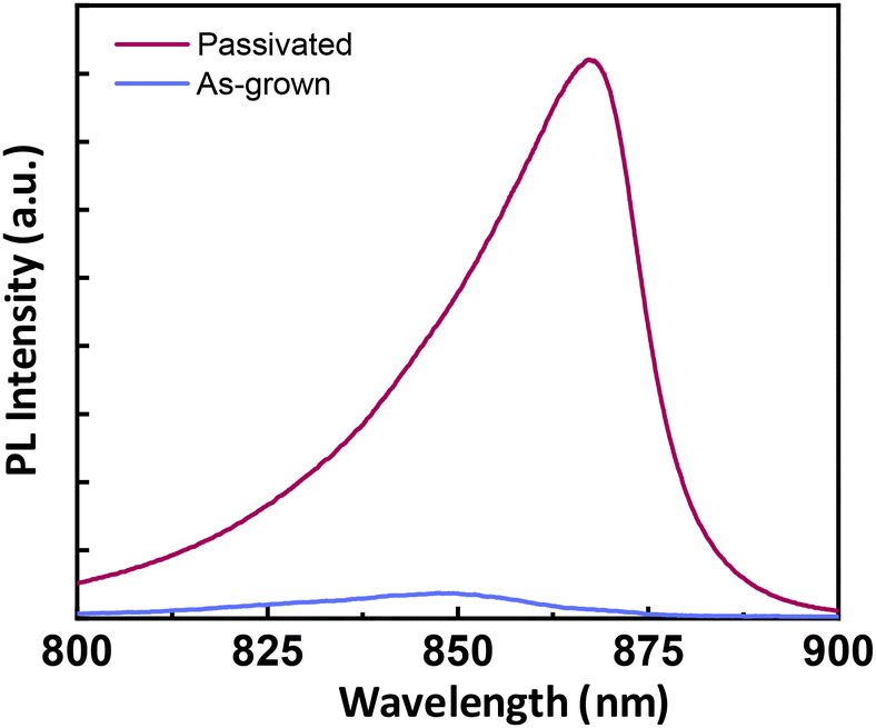 | ||
| Fig. 1 Comparison of average micro-PL spectra between passivated intrinsic nanowires and pristine intrinsic nanowires. | ||
The PL quenching could be a result of the type-II band alignment between the passivation shell and inner semiconductor materials, which is related to the efficient separation of photogenerated carriers and effective reduction in radiative recombination. However, this normally happens with thick shells. In our case, the passivation layer is ultra-thin. To the best of our knowledge, there is still the lack of a report about a band alignment diagram between ultrathin ZnO and GaAs, but it is believed to be difficult to form a clear type-II band alignment. Here, ALD ZnO efficiently suppresses oxide formation and minimizes Fermi-level pinning. The greatly improved PL intensity demonstrates that the passivation effect is dominant and PL quenching by type-II band alignment is not the main concern in this structure.
As shown in Fig. 2(a), Cr/Au electrodes are deposited on the two ends of a single p-type GaAs nanowire, and the heavily p-doped silicon substrate serves as the back gate. The SEM image shows a single NW-based device (Fig. 2(b)). The current becomes larger with source–drain bias with bending characteristics, caused by a back-to-back Schottky configuration. Although the back gate modulation role is insufficient, as displayed in Fig. 2(c), the output characteristics under the illumination of a microscope still confirm the p-type conductivity of a GaAs nanowire. The gate voltage varies from −30 V to +30 V with a step of 10 volts. The accumulation of holes inside the nanowire channel occurs under a negative gate voltage, which raises the drain current. The case of positive gate bias tends to deplete majority carriers, which reduces the drain current.
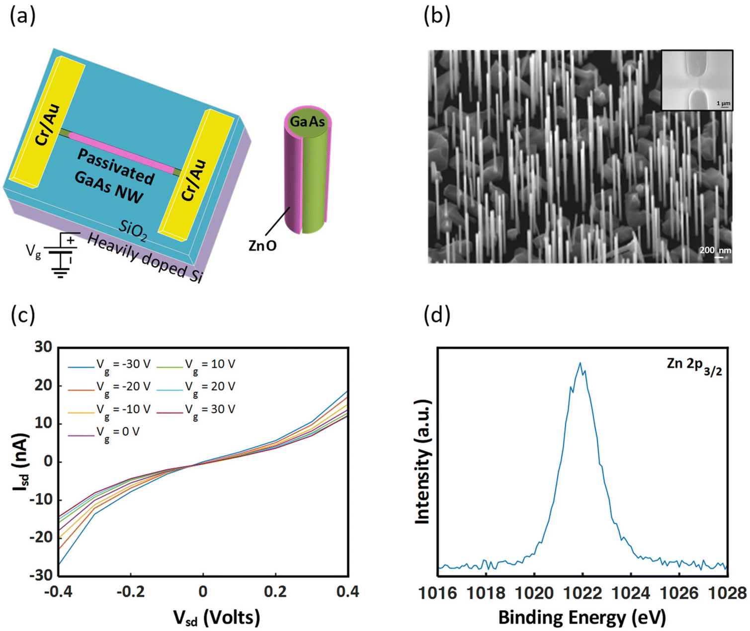 | ||
| Fig. 2 (a) Device schematic. (b) SEM image of the GaAs nanowires. (The inset shows the SEM image of the GaAs nanowire photodetector.) (c) Output characteristics of NW FET under different gate biases. (d) XPS Zn 2p spectra. | ||
The existence of ZnO on the substrate can be confirmed by XPS Zn 2p spectra whose peak is located at about 1022 eV, and this peak relates to the Zn–O bond (Fig. 2(d)). Characterization of the presence of ZnO was also performed by PL and Raman tests, but they do not work for capturing such a weak signal, due to its ultrathin nature. The chemical etching behavior of ZnO could refer to reference,36 which shows that the etching rate of ZnO by HCl is very fast. In this article, ZnO present in the source/drain part is etched away by diluted hydrochloric acid.
The dark current Id without gate bias under forward- and reverse-biased voltages is slightly different, which may originate from unequal Schottky barrier heights at the two ends. Compared with the reference device in our previous report,33 its dark current increases at the same bias voltage. A similar phenomenon, referred to as conductivity improvement, has been found in previous literature,18,37–39 determined by reduction in surface trap density.
The surface states on p-GaAs nanowires act as recombination centers for free carriers and positively charged surface traps.40 A depletion shell exists and the effective channel available for carrier transport is narrowed and confined, because of the surface states.41 XPS spectral analysis, which could reflect interfacial chemical bonding, was utilized to evaluate the results on (In)GaAs substrates by an ALD ZnO passivation layer.31,32 A substantial decrease in As–As bonding and a drop in Ga–O bonding were observed. The strong Zn–O bond strength induces a nearly impossible reaction between oxygen atoms in ZnO and Ga(As) atoms,42 and the conformal dense coverage of ZnO effectively suppresses the penetration of oxygen from the atmosphere into NWs. Besides, the Au/Zn/Au structure is one option for GaAs Ohmic contact, as Zn could serve as a p-type dopant.43 Hence, suppression of nanowire conductivity induced by Fermi level pinning could be alleviated in part, via the introduction and diffusion of Zn atoms. The improvement in the conductivity of photodetectors enables better photocurrent transportation, making a boost in photoresponsivity possible.44
The optoelectronic performance of the modified device without gate voltage is plotted in Fig. 3. The net photocurrent is defined by Iph = Ilight − Id, where Ilight denotes the current under illumination. The device shows a distinct photocurrent even under a very weak illumination. Generally, the current increases as illumination intensity becomes larger. The photoresponsivity is defined by R = Iph/PA, where P means the incident light intensity per unit area, and A is the effective illuminated area associated with nanowire geometric size and channel length. The spectral responsivity rises with increasing bias. Additionally, the specific detectivity is calculated with the formula D* = R(A/2eIdark)1/2, where e is the electron charge. Moreover, another vital parameter named the optical gain, which is related to the electron–hole pair quantity collected by the electrodes upon excitation by one incident photon, is defined as G = R × hc/λe, where h denotes the Planck constant, c is the speed of light, and λ means the wavelength of the irradiation light. The relationship of responsivity versus incident power is plotted in Fig. 3(b). It is clearly shown that the photoresponsivity drops with increasing incident power density, and the variation trend of the specific detectivity is the same. These two parameters can reach 946 kA W−1 and 3.93 × 10¹⁴ Jones, respectively, when illuminated by 21 μW cm−2 532 nm light.
 | ||
| Fig. 3 Optoelectronic performance at zero gate bias (a) output characteristics of a nanowire photodetector under 532 nm wavelength light for different intensities. (b) Dependence of the photocurrent and responsivity on incident illumination density at 1 V bias voltage. (c) Variation of photocurrent with light intensity for various bias voltages. (d) Dark current comparison between the devices with and without ZnO in the source/drain part. | ||
To obtain a further understanding of the photodetector performance, the working principle of the device is discussed here. Limited by the Fermi level pinning at one-third of the bandgap above the valence band maximum, the Schottky barrier height is usually fixed regardless of the metal work function. The difference in negative work function between Cr and p-type GaAs leads to downward band-bending at the GaAs NW/metal contact interface. A layer of negative charges forms in the GaAs side, while a layer of positive charge is built in the metal region. One Schottky junction is forward-biased, just acting as a resistor in series, while the other is reverse-biased on which most of the voltage drop is applied. A built-in electric field inside the reverse-biased Schottky junction could suppress the recombination rate of photon-generated electron–hole pairs or separate the photon-generated electron–hole pairs efficiently.39 The Schottky barrier height could be extracted from the following formula:

The peak of the photo-response ratio expressed by Iph/Id is about 12.56, under 780 nm light with a power of 3 mW cm−2. It becomes large with an increase in light power, due to the creation of more photo-generated carriers. The light-intensity-dependent photocurrent under different biases is displayed in Fig. 3(c) and could be fitted using a power law, Iph ∝ Pα, where the extracted component α could indicate the type of photogeneration mechanism. The photocurrent increases with applied bias. Generally speaking, the photocurrent is dominated more by the photoconductive effect when the component approaches 1, and a sub-linear relationship indicates the presence of some complex photogeneration and recombination processes.49 The less depleted channel produces a smaller α value, which is consistent with other reports.47 The decrease in α dependence on bias is possibly induced by the effect of defects on carrier transportation.50 Stronger illumination induces larger carrier concentration near the Schottky area, resulting in a reduced built-in electric field and weakened carrier separation efficiency. Limited to the small effective illuminated area of a single nanowire and the inherent property of a single GaAs nanowire device, it is hard to get a very distinct photo-response ratio like other materials, which is consistent with other papers on GaAs nanowire photodetectors.33,44,47
I–V measurements were conducted on a nanowire device without removal of ZnO before metal contact deposition, as shown in Fig. 3(d), and one possible source is responsible for a low current. The existence of an energy barrier caused by an interface valence band offset hinders carrier collection by metal electrodes.
A comparison of device performance is given in Table 1. Since the passivation alleviates the surface states and leaves more free photocarriers, the role of the Schottky junctions in the photogeneration mechanism may thus be reasonably dominant in photoresponse enhancement. The passivated device exhibits ultrahigh and broadband responsivity to weak light, considerable detectivity, and a normal photoresponse ratio. This superior behavior could be attributed to three factors: (1) the high-quality crystal of self-catalyzed GaAs nanowires ensures lower numbers of nonradiative recombination centers and carrier traps. (2) The ZnO passivation could effectively reduce the surface states present in GaAs and improve conductance, enabling better photocurrent transportation. (3) A reverse-biased Schottky junction broadens the barrier width and strengthens the built-in electric field, which promotes the separation of photo-generated carriers and results in high photoresponsivity.
| Material | Wavelength (nm) | Bias (V) | Dark current | Photoresponsivity (A W−1) | Specific detectivity (Jones) | Optical gain (%) | Ref. |
|---|---|---|---|---|---|---|---|
| Si-doped GaAs NW | 532 | −1 | ∼50 pA | 1175 | 3.02 × 10¹² | 2.74 × 10⁵ | 44 |
| Thiourea-passivated GaAsSb NW | 1550 | 2 | 1.3 μA | 5.4 × 10⁴ | 2.5 × 10¹⁰ | 4.4 × 10⁶ | 45 |
| Sulfur-passivated undoped GaAs NW | 532 | 1 | 0.07 pA | 25 | 9.04 × 10¹² | — | 46 |
| Sulfur-passivated p-GaAs NW | 520 | 2 | 22.2 μA | 6.4 × 10⁵ | 8.2 × 10¹² | 1.5 × 10⁸ | 47 |
| p-GaAs NW (reference device) | 632.8 | −5 | 4 nA | 1.45 × 10⁵ | 1.48 × 10¹⁴ | 2.85 × 10⁷ | 33 |
| Passivated p-GaAs NW | 532 | 1 | 21.97 nA | 9.46 × 10 5 | 3.93 × 10 14 | 2.2 × 10 8 | This work |
4. Conclusions
In summary, the passivation efficacy of ZnO deposition on the intrinsic GaAs nanowires was investigated, and a surface-modified high-quality doped GaAs nanowire photodetector with outstanding performance was demonstrated. The PL enhancement and increase in conductance after ZnO treatment prove its vital role in reducing surface recombination velocity and surface state density as a surface passivation treatment. The dramatic elimination of the surface states upon passivation ensures good photoconductance, and the low growth temperature of ZnO allows such a passivation procedure, which is more compatible with modern semiconductor device processing techniques. Compared to the pristine device in our previous report, the photoresponsivity is found to be extraordinarily enhanced up to 946 kA W−1, and it shows a considerable specific detectivity under 532 nm light. This device configuration opens a new gateway for enhancing photodetector performance with high responsivity, detectivity and optical gain, which is expected to be extended to other types of low-dimensional semiconductor materials.Author contributions
All authors contributed to the writing of the manuscript. Additionally, Fuxiang Shang: conceptualization, investigation, formal analysis, writing original draft; Chaofei Zha: investigation, formal analysis; Hanchen Zhu: investigation, data curation; Zheyu Zhang: methodology; Yuanhao Shen: investigation; Qichao Hou: investigation; Linjun Zhang: conceptualization; Yanmeng Chu: data curation; Lulu Chen: investigation; Junjie Zhao: resources; Wenzhang Fang: resources; Huiyun Liu: resources; Yishu Zhang: resources; Zhiyuan Cheng: supervision, funding acquisition, project administration; Yunyan Zhang: supervision, funding acquisition, project administration.Conflicts of interest
There are no conflicts to declare.Acknowledgements
We thank Chao Bi from Core Facilities, Zhejiang University School of Medicine for their technical support, acknowledge the support of Dr. Jiabao Sun (assistance during magnetron sputtering), Ying Sun, and Shijian Xie from the Micro-Nano Fabrication Centre of Zhejiang University, and thank Dr. Huan Zhang from Instrumentation and Service Center for Physical Sciences at Westlake University for the supporting in XPS measurement. This work was supported under Zhejiang Provincial Natural Science Foundation of China (Z24F040009), Zhejiang University Education Foundation Qizhen Scholar Foundation (K20240015), and CMOS Special Program of Zhejiang University (04010000-K2A033208).References
- Y. Zhang, J. Wu, M. Aagesen and H. Liu, J. Phys. D: Appl. Phys., 2015, 48, 463001 CrossRef.
- Y. Zhang and H. Liu, Crystals, 2019, 9, 87 CrossRef.
- X. Yuan, D. Pan, Y. Zhou, X. Zhang, K. Peng, B. Zhao, M. Deng, J. He, H. H. Tan and C. Jagadish, Appl. Phys. Rev., 2021, 8, 2 Search PubMed.
- W. Wu, Y. Li, L. Liang, Q. Hao, J. Zhang, H. Liu and C. Liu, J. Phys. Chem. C, 2019, 123, 14781–14789 CrossRef CAS.
- L. Gao, K. Zeng, J. Guo, C. Ge, J. Du, Y. Zhao, C. Chen, H. Deng, Y. He and H. Song, Nano Lett., 2016, 16, 7446–7454 CrossRef CAS PubMed.
- X. Zhang, Q. Liu, B. Liu, W. Yang, J. Li, P. Niu and X. Jiang, J. Mater. Chem. C, 2017, 5, 4319–4326 RSC.
- G. Li, R. Gao, Y. Han, A. Zhai, Y. Liu, Y. Tian, B. Tian, Y. Hao, S. Liu and Y. Wu, Photonics Res., 2020, 8, 1862–1874 CrossRef CAS.
- R. Chen, L. Li, L. Jiang, X. Yu, D. Zhu, Y. Xiong, D. Zheng and W. Yang, Nanotechnology, 2022, 33, 135707 CrossRef PubMed.
- G. Lin, D. Liang, C. Yu, H. Hong, Y. Mao, C. Li and S. Chen, Opt. Express, 2019, 27, 32801–32809 CrossRef CAS PubMed.
- J. He, Z. Huang, Z. Li, W. W. Wong, Y. Yu, L. Huang, X. Li, L. Fu, H. H. Tan and C. Jagadish, J. Phys. D: Appl. Phys., 2022, 56, 015105 CrossRef.
- X. Zuo, Z. Li, W. W. Wong, Y. Yu, X. Li, J. He, L. Fu, H. H. Tan, C. Jagadish and X. Yuan, Appl. Phys. Lett., 2022, 120, 7 CrossRef.
- H. I. H. Ito and T. I. T. Ishibashi, Jpn. J. Appl. Phys., 1994, 33, 88 CrossRef CAS.
- A. C. Chia and R. R. LaPierre, J. Appl. Phys., 2012, 112, 6 CrossRef.
- D. Ren, K. M. Azizur-Rahman, Z. Rong, B.-C. Juang, S. Somasundaram, M. Shahili, A. C. Farrell, B. S. Williams and D. L. Huffaker, Nano Lett., 2019, 19, 2793–2802 CrossRef CAS PubMed.
- L. Black, A. Cavalli, M. Verheijen, J. Haverkort, E. Bakkers and W. Kessels, Nano Lett., 2017, 17, 6287–6294 CrossRef CAS PubMed.
- M. Milojevic, C. Hinkle, F. Aguirre-Tostado, H. Kim, E. Vogel, J. Kim and R. Wallace, Appl. Phys. Lett., 2008, 93, 25 Search PubMed.
- M. V. Lebedev, Y. M. Serov, T. V. Lvova, R. Endo, T. Masuda and I. V. Sedova, Appl. Surf. Sci., 2020, 533, 147484 CrossRef CAS.
- P. A. Alekseev, M. S. Dunaevskiy, V. P. Ulin, T. V. Lvova, D. O. Filatov, A. V. Nezhdanov, A. I. Mashin and V. L. Berkovits, Nano Lett., 2015, 15, 63–68 CrossRef CAS PubMed.
- J. Shen, H. Chen, J. He, Y. Li, X. Yang, M. Zhu and X. Yuan, Appl. Phys. Lett., 2024, 124, 12 Search PubMed.
- S.-H. Kim, G.-S. Kim, S.-W. Kim, J.-K. Kim, C. Choi, J.-H. Park, R. Choi and H.-Y. Yu, IEEE Electron Device Lett., 2016, 37, 373–376 CAS.
- N. Tajik, C. Haapamaki and R. LaPierre, Nanotechnology, 2012, 23, 315703 CrossRef CAS PubMed.
- V. Raj, H. H. Tan and C. Jagadish, Appl. Mater. Today, 2020, 18, 100503 CrossRef.
- T. K. O. Vu, M. T. Tran and E. K. Kim, J. Alloys Compd., 2022, 924, 166531 CrossRef.
- Y. Chen, C. Zheng, L. Hu and Y. Chen, J. Alloys Compd., 2019, 775, 1213–1220 CrossRef CAS.
- D. P. Pham, S. Lee, S. Kim, S. Chowdhury, M. Q. Khokhar, A. H. T. Le, Y. Kim, J. Park and J. Yi, Mater. Sci. Semicond. Process., 2021, 121, 105344 CrossRef CAS.
- S. Kundu, T. Shripathi and P. Banerji, Solid State Commun., 2011, 151, 1881–1884 CrossRef CAS.
- Y. Zhu, V. Raj, Z. Li, H. H. Tan, C. Jagadish and L. Fu, Adv. Mater., 2021, 33, 2105729 CrossRef CAS PubMed.
- V. V. Ursaki, S. Lehmann, V. V. Zalamai, V. Morari, K. Nielsch, I. M. Tiginyanu and E. V. Monaico, Crystals, 2022, 12, 1145 CrossRef CAS.
- M. Kolhep, F. Pantle, M. Karlinger, D. Wang, T. Scherer, C. Kübel, M. Stutzmann and M. Zacharias, Nano Lett., 2023, 23, 6920–6926 CrossRef CAS PubMed.
- N. Gagrani, K. Vora, L. Fu, C. Jagadish and H. H. Tan, Nanoscale Horiz., 2022, 7, 446–454 RSC.
- Y.-C. Byun, S. Choi, Y. An, P. C. McIntyre and H. Kim, ACS Appl. Mater. Interfaces, 2014, 6, 10482–10488 CrossRef CAS PubMed.
- C. Liu, H. Lü, T. Yang, Y. Zhang, Y. Zhang, D. Liu, Z. Ma, W. Yu and L. Guo, Appl. Surf. Sci., 2018, 444, 474–479 CrossRef CAS.
- H. Ali, Y. Zhang, J. Tang, K. Peng, S. Sun, Y. Sun, F. Song, A. Falak, S. Wu and C. Qian, Small, 2018, 14, 1704429 CrossRef PubMed.
- J. Fouache and D. Lincot, Appl. Surf. Sci., 2000, 153, 223–234 CrossRef.
- E. V. Skopin, L. Rapenne, H. Roussel, J.-L. Deschanvres, E. Blanquet, G. Ciatto, D. D. Fong, M.-I. Richard and H. Renevier, Nanoscale, 2018, 10, 11585–11596 RSC.
- J. Hüpkes, J. I. Owen, S. E. Pust and E. Bunte, ChemPhysChem, 2012, 13, 66–73 CrossRef PubMed.
- Y. Jiang, R. Shen, T. Li, J. Tian, S. Li, H. H. Tan, C. Jagadish and Q. Chen, Nanoscale, 2022, 14, 12830–12840 RSC.
- N. Tajik, A. Chia and R. LaPierre, Appl. Phys. Lett., 2012, 100, 20 CrossRef.
- J. Miao, W. Hu, N. Guo, Z. Lu, X. Zou, L. Liao, S. Shi, P. Chen, Z. Fan and J. C. Ho, ACS Nano, 2014, 8, 3628–3635 CrossRef CAS PubMed.
- K.-i. Seo, S. Sharma, A. A. Yasseri, D. R. Stewart and T. I. Kamins, Electrochem. Solid-State Lett., 2006, 9, G69 CrossRef CAS.
- O. Demichel, M. Heiss, J. Bleuse, H. Mariette and A. Fontcuberta i Morral, Appl. Phys. Lett., 2010, 97, 20 CrossRef.
- Y. Lan, G. Yang, Y. Zhao, Y. Liu and A. Demir, Appl. Surf. Sci., 2022, 596, 153506 CrossRef CAS.
- A. Baca, F. Ren, J. Zolper, R. Briggs and S. Pearton, Thin Solid Films, 1997, 308, 599–606 CrossRef.
- X. Chen, D. Wang, T. Wang, Z. Yang, X. Zou, P. Wang, W. Luo, Q. Li, L. Liao and W. Hu, ACS Appl. Mater. Interfaces, 2019, 11, 33188–33193 CrossRef CAS PubMed.
- W. Wang, S. Yip, Y. Meng, W. Wang, F. Wang, X. Bu, Z. Lai, X. Kang, P. Xie and Q. Quan, Adv. Opt. Mater., 2021, 9, 2101289 CrossRef CAS.
- X. Chen, N. Xia, Z. Yang, F. Gong, Z. Wei, D. Wang, J. Tang, X. Fang, D. Fang and L. Liao, Nanotechnology, 2018, 29, 095201 CrossRef PubMed.
- X. Li, X. Yu, H. Zeng, G. Boras, K. Shen, Y. Zhang, J. Wu, K. L. Choy and H. Liu, Appl. Phys. Lett., 2021, 119, 5 Search PubMed.
- S. Thunich, L. Prechtel, D. Spirkoska, G. Abstreiter, A. Fontcuberta i Morral and A. W. Holleitner, Appl. Phys. Lett., 2009, 95, 8 CrossRef.
- R. Nur, T. Tsuchiya, K. Toprasertpong, K. Terabe, S. Takagi and M. Takenaka, Commun. Mater., 2020, 1, 103 CrossRef.
- H. Wang, Appl. Phys. Lett., 2013, 103, 9 Search PubMed.
| This journal is © The Royal Society of Chemistry 2024 |