
 Open Access Article
 This Open Access Article is licensed under a
 Creative Commons Attribution 3.0 Unported Licence
A high density nanopore 3-triangulene kagome lattice†
Pedro Elias Priori
Spalenza
 a,
Fábio Arthur Leão
de Souza
b,
Rodrigo G.
Amorim
c,
Ralph H.
Scheicher
*d and
Wanderlã Luis
Scopel
a
a,
Fábio Arthur Leão
de Souza
b,
Rodrigo G.
Amorim
c,
Ralph H.
Scheicher
*d and
Wanderlã Luis
Scopel
a
aDepartamento de Física, Universidade Federal do Espírito Santo – UFES, Vitória, ES, Brazil. E-mail: pedro.spalenza@edu.ufes.br
bInstituto Federal de Educação, Ciância e Tecnologia do Espírito Santo – IFES, Ibatiba, ES, Brazil. E-mail: fabio.souza@ifes.edu.br
cDepartamento de Física, ICEx, Universidade Federal Fluminense – UFF, Volta Redonda, RJ, Brazil. E-mail: rgamorim@id.uff.br
dDivision of Materials Theory, Department of Physics and Astronomy, Uppsala University, Box 516, SE-751 20 Uppsala, Sweden. E-mail: ralph.scheicher@physics.uu.se
First published on 11th April 2024
Abstract
Nanopore-containing two-dimensional materials have been explored for a wide range of applications including filtration, sensing, catalysis, energy storage and conversion. Triangulenes have recently been experimentally synthesized in a variety of sizes. In this regard, using these systems as building blocks, we theoretically examined 3-triangulene kagome crystals with inherent holes of ∼12 Å diameter and a greater density array of nanopores (≥1013 cm−2) compared to conventional 2D systems. The energetic, electronic, and transport properties of pristine and B/N-doped 3-triangulene kagome crystals were evaluated through a combination of density functional theory and non-equilibrium Green's function method. The simulated scanning tunneling microscopy images clearly capture electronic perturbation around the doped sites, which can be used to distinguish the pristine system from the doped systems. The viability of precisely controlling the band structure and transport properties by changing the type and concentration of doping atoms is demonstrated. The findings presented herein can potentially widen the applicability of these systems that combine unique electronic properties and intrinsically high-density pores, which can pave the way for the next generation of nanopore-based devices.
1. Introduction
Since the isolation of graphene,1 two-dimensional (2D) systems have paved the way for designing and fabricating novel materials. Recently, the production of nanoflakes2 based on aromatic rings has received great attention due to the possibility of fabricating tailored materials for applications of 2D nanodevices. In this sense, graphene nanoflakes with a triangular shape, called n-triangulene3–6 (n being the number of benzoic rings on a side), have been used as a building block for creating more complex structures.7–9The synthesis of unsubstituted triangulenes is a difficult task due to the presence of unpaired electrons and due to their highly reactive edges. However, Allinson10 and Taylor11 overcame these issues with the addition of substituents, which permitted their stabilization and synthesis. Recently, experimental breakthroughs have opened routes to the on-surface synthesis (such as on Cu(111), NaCl(100), Xe(111), and Au(111)) of unsubstituted triangulenes utilizing different precursors and techniques, allowing the synthesis of molecules,3 dimers,7 chains8 and nanostars.9
A promising way to tune the electronic and magnetic properties of triangulenes is through doping and edge passivation.12,13 Kan et al.14 have studied isolated 3-triangulene and demonstrated that it is possible to manipulate the occupation of π orbitals by replacing the central carbon atom with nitrogen or boron. They have also explored triangulene crystals and showed through the use of density functional theory (DFT) calculations that N-doping tunes the magnetic order from antiferromagnetic to ferromagnetic. In addition, Chen et al. have reported a facile synthesis of replacing the carbon edges of 4-triangulene with three oxygen–boron–oxygen (OBO) units, and the results suggest that these kinds of molecules hold promising potential for optical applications and can be a route to creating OBO-doped 2D materials.15
2D crystals derived from substituted12,16–20 and non-substituted21,22 triangulenes have also been explored. Steiner et al.18 successfully fabricated a 2D covalent kagome network architecture based on carbonyl-functionalized pores on the Au(111) surface. The system was characterized through a combination of scanning tunneling microscopy (STM) and DFT calculations, which showed that it is weakly bound to the substrate and its electronic structure is kept unperturbed. Interestingly, a periodic membrane with intrinsic holes can be produced using triangulenes as building blocks. In particular, nanopores in 2D materials have potential applications in DNA, protein and biomolecule sensing,23–25 desalination,26–28 the petrochemical industry29,30 and others.20,31,32
In this work, through DFT combined with non-equilibrium Green's function (NEGF), we explored the structural, electronic, and electronic transport properties of pristine and B/N-doped 3-triangulene kagome lattices. A systematic investigation of the central carbon atom of triangulenes substituted with B or N was performed via calculation of the formation energy, which is governed by an exothermic process. STM images were obtained and the results show the difference between the doped and pristine systems. The results also show that band dispersion around the Fermi level can be precisely controlled by varying the type of dopant and its concentration. Finally, the zero-bias transmission of the B/N-doped systems shows an increase in the number of transmission channels at the Fermi level compared to the pristine system. Thus, our findings suggest these systems as highly promising potential candidates for nanopore-based devices.
2. Methodology
Atomic structure optimization, energetic stability, and electronic property calculations were performed using DFT.33,34 The exchange–correlation energy was described within the generalized gradient approximation (GGA) proposed by Perdew, Burke, and Ernzerhof (PBE),35 as implemented in Quantum ESPRESSO.36,37 The interaction between ions and valence electrons was described by projector augmented wave pseudopotentials (PAW),38,39 and the energy cutoff was set to 650 eV. All structures were relaxed until Hellmann–Feynman forces acting on each atomic component were smaller than 0.05 eV Å−1. An orthorhombic unit cell of 29.83 Å × 17.22 Å × 15.00 Å dimensions was used with a sufficiently large vacuum gap in the z-direction in order to avoid interactions between periodic images. The Brillouin zone integration was performed using the Monkhorst–Pack scheme40 with 5 × 5 × 1 grids.We also carried out DFT calculations as implemented in the SIESTA41,42 package. The core electrons were described by norm-conserving Troullier–Martins pseudopotentials,43 and a double-zeta polarized (DZP) basis set44 was considered. A real-space mesh cutoff (300 Ry) and 2 × 2 × 1 k-point grids were used. The Tersoff–Hamann STM45 model was used, where the tip is assumed to be of s-orbital type, and the tunneling current is proportional to the local density of states (LDOS). In this approach, the sum is over all Kohn–Sham states in the energy windows (EF, EF − V) and (EF, EF + V) for occupied and unoccupied states, respectively, in which the isosurfaces of the LDOS can be correlated with them at a constant height. V is the applied bias and EF is the Fermi energy.
Transport calculations were carried out with the TranSIESTA code,46,47 which combines DFT and NEGF, and the schematic model used is shown in Fig. 1(b). For solving the electronic transport problem, Green's function was used and is defined as below:
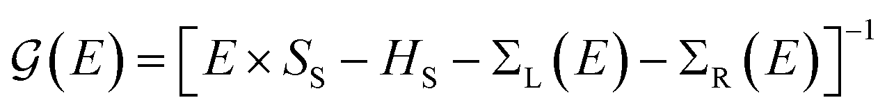 | (1) |
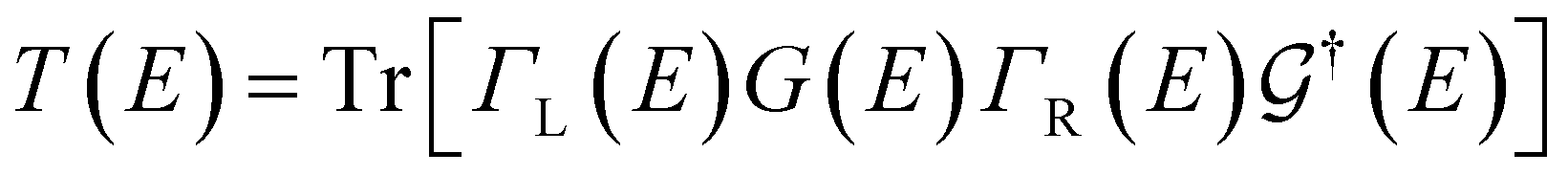 | (2) |
 is the retarded (advanced) Green's function. We have carried out zero-bias calculations, which lead to zero electrical currents. Further details can be found elsewhere.46,47
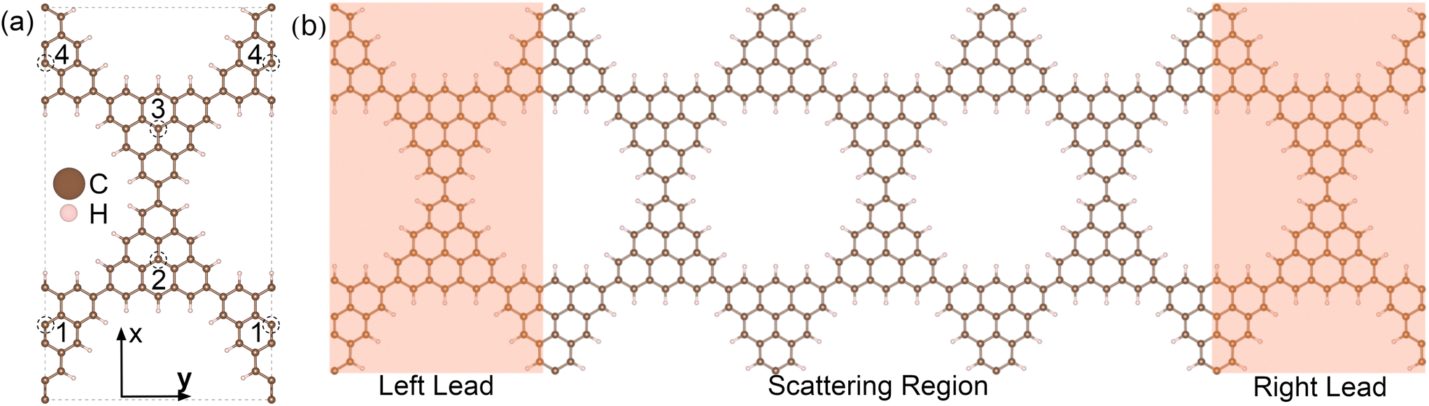 | ||
| Fig. 1 (a) Fully relaxed geometry of the rectangular unit cell of the 3-triangulene kagome, where doping sites are indicated by numbers 1–4. Brown and light pink color spheres represent the C and H atoms, respectively. (b) Schematic setup of electronic transport along the y-direction. The dimensions of the scattering region (electrodes) are 29.83 Å (29.83 Å) wide and 51.66 Å (17.22 Å) long. The scattering regions for each of the studied structures are depicted in Fig. S2 and S3 in the ESI.† | ||
3. Results
The schematic crystalline structure of the 3-triangulene kagome is shown in Fig. 1(a), and the atomic sites that will be doped with either boron or nitrogen are highlighted by dashed circles and labeled with the numbers 1–4, where dashed grey lines show the unit cell. Interestingly, regarding the graphene domain, sites 1 and 3 (2 and 4) belong to sublattice A (B). These doping sites were motivated by success in multiple experiments in similar systems.16–19,48 From the 3-triangulene relaxed atomic structure, we found that the C–C bond lengths vary from 1.40 Å to 1.43 Å, and C–H bond length was found to be 1.09 Å. The nanopore density was determined by calculating the number of pores per unit area. The density of 3.89 × 1013 cm−2 for the 3-triangulene kagome represents a notably high value for pore density.49Fig. 2 shows the electronic band structure of the 3-triangulene kagome (black solid lines), where one notes flat bands appearing roughly at ±0.2 eV, which are ascribed to carbon pz orbitals (as can be seen in Fig. S1 of the ESI†). Additionally, a Dirac cone around the Fermi level along the Y → Γ direction (corresponding to the zigzag direction of the crystals) is also observed. These features are typical signatures of the kagome lattice, as previously reported.22
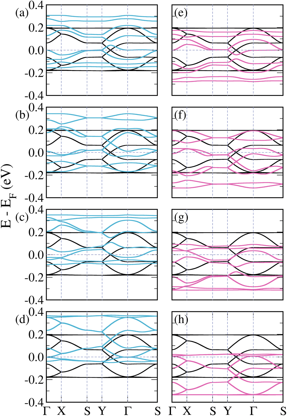 | ||
| Fig. 2 Band structures of pristine (black lines) and doped 3-triangulene kagome lattices: (a)–(d) doping atomic sites 1–4 with boron (light blue lines) and (e)–(h) doping sites 1–4 with nitrogen (pink lines); as labeled in Fig. 1. | ||
Wang et al. have experimentally demonstrated that the substitution of the central carbon atom of 3-triangulene on a metal surface (Ag and Au) can substantially modify the electronic and magnetic properties of the system.48 In addition, Anindya et al. found21 that B/N doping on the triangulene kagome lattice permitted control of the electronic/magnetic properties of 3-triangulene crystals. In this context, the energetic stability of substitutional defects in the 3-triangulene kagome was explored and their formation energy per atom (Eform) was calculated using the equation:
 | (3) |
Table 1 shows that for all studied concentrations and for both dopants (B and N), the system formation is governed by an exothermic process. A linear increment of the formation energy with the number of doping atoms for both dopant species is observed (as presented in Fig. S4 of the ESI†), following the same tendency of previous reports.50,51 For the B-doped system, the formation energy varies from −5.4 meV per atom up to −22.0 meV per atom, while N doping varies from −41.9 meV per atom to −169.0 meV per atom. This verifies that doping induces a small structural disorder of the C–C (<0.04 Å) and C–H distances far from the doped sites compared to pristine ones, where the internuclear separations of the B-doped (N-doped) systems C–B (C–N) are 1.47 (1.39) Å, which agree very well with B- and N-doped graphene.52
| Number of dopants | E form (meV per atom) | |
|---|---|---|
| B-doping | N-doping | |
| 1 | −5.4 | −41.9 |
| 2 | −11.0 | −84.3 |
| 3 | −16.7 | −126.8 |
| 4 | −22.0 | −169.0 |
Fig. 2(a)–(d) show the band structures of the 3-triangulene kagome doped with boron atoms at atomic sites 1–4, as labeled in Fig. 1. B-doping induces a systematic shift of bands toward higher energies in comparison with the pristine one (black curves) with increasing doping concentration (from Fig. 2(a)–(d)), resulting in a p-doping-like effect. In all cases, the number of bands crossing the Fermi level increases. Interestingly, the Dirac cone (Y to Γ) is preserved, as observed in Fig. 2(b) and (d), whereas in Fig. 2(a) and (c) it is opened. In the case of N-doping, one observes a systematic shift of the bands to lower energy compared to the pure ones, which characterizes the n-doping effect. For the Y–Γ path, one notes in Fig. 2(f) and (h) that the Dirac cone is preserved, while in Fig. 2(e) and (g) the Dirac cone opens. As a result, for both B- and N-doping, an opening of the Dirac cone is observed when the number of doped sites in sublattices A and B are different. On the other hand, when the numbers of doped sites in sublattices A and B are equal, the Dirac cone is preserved, with only a shift toward higher (lower) energies in the B-doped (N-doped) case. These results suggest that by varying the kind and concentration of doping, band dispersion around the Fermi level can be precisely controlled. It is important to highlight that for the case where the unit cell is doped twice, there are two possible configurations (as shown in the ESI, Fig. S5†). Fig. 2(b) and (f) only show the case where sites 1 (sublattice A) and 2 (sublattice B) are doped; the other case (when sites 1 (sublattice A) and 3 (sublattice A) are doped) is shown in the ESI, Fig. S6†. A similar trend of opening and closure of the Dirac cone was observed for pristine graphene.53
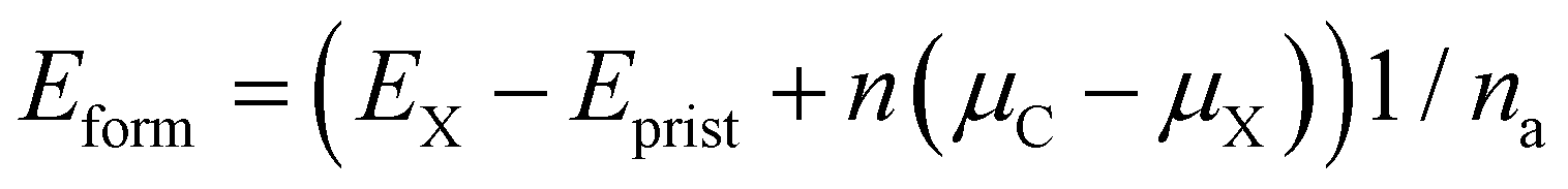
To better understand the effect of B/N doping on the surface at the atomic scale, Fig. 3 shows simulated STM images for the 3-triangulene kagome and its doped counterparts, the most energetically favorable ones (4B-doped and 4N-doped). We simulated the filled (empty) states by integrating charge density from the Fermi level to −1.0 (+1.0) eV, and the images were obtained considering the constant-height mode. The aforementioned energy ranges are where dopant energy levels appear (as shown in Fig. S7†). Fig. 3(a) and (b) show the pristine 3-triangulene kagome and 4B-doped systems for occupied states, while Fig. 3(c) and (d) present the pristine and 4N-doped systems for an unoccupied state, respectively. The STM images for occupied and unoccupied states differ in the linkage between the two neighboring triangles. For the undoped ones, we note two well-defined charge lobules for occupied state 3 (a), and in the case of unoccupied state 3 (c), there are four lobules linking the triangles. Fig. 3(b) shows a B-doped system, where the three brightest spots in the center of the triangles appear as a continuum triangular shape, once a boron atom, by Bader's analysis,54,55 donates one electron to each of its first neighbors, as expected due to carbon possessing higher electronegativity. On the other hand, for the N-doped system, the effect is different once the N atom is the acceptor and C is the donator, as shown in Fig. 3(d). The results clearly show that doped systems can be distinguished from pristine ones in both situations, as the bright patterns in the vicinity of doped sites change significantly in shape. Our results of the simulated STM image for the freestanding 3-triangulene kagome are locally comparable with triangulene dimers on Au (111) surface.7
 | ||
| Fig. 3 Simulated STM images of occupied states (−1.0 eV up to EF): (a) pristine and (b) B-doped 3-triangulene kagome lattices. Unoccupied state (EF up to +1.0 eV) STM images are shown for the pristine 3-triangulene kagome (c) and N-doped (d) one. | ||
The focus will now be on the 3-triangulene kagome lattice's electronic transport properties and how 4B- and 4N-doping affects them. Fig. 4(b) presents the zero bias transmission curves for pristine (black curve), 4N-doped (pink curve), and 4B-doped lattices (light blue). For the pristine case, we observe two quite symmetrical peaks around the Fermi level. As expected from the band structure analysis, N-doping (B-doping) induces a shift of the two corresponding peaks toward lower (higher) energies. As a result, an increase in the number of transmission channels at the Fermi level is observed for both doped cases. Additionally, we observed the emergence of two new peaks in the transmission spectra of the 4B-doped system at −0.045 eV and 0.334 eV, and one new peak at 0.035 eV for the 4N-doped case. To understand the origin of these new peaks in the transmission of doped systems, one needs to keep in mind that in the band structure of the pristine system, there are two degenerated flat bands at −0.18 eV and another two at +0.19 eV, and that these flat bands do not contribute to transport initially. However, in the 4B-doped band structure (Fig. 2(d)), one can verify that the bands, which correspond to the flat bands of the pristine system, become less energetically localized and their degeneracy is lifted around the Gamma point. For the 4N-doped case, the same effect described above for the 4B-doped is observed for the band at 0.035 eV. Such circumstances are responsible for the two (one) extra peaks in the 4B-doped (4N-doped) transmission when compared to the pristine one.
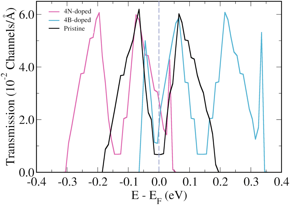 | ||
| Fig. 4 Energy resolved zero bias transmission for the pristine (black lines), B-doped (light blue lines), and N-doped lattices (pink lines) of 3-triangulene kagome. | ||
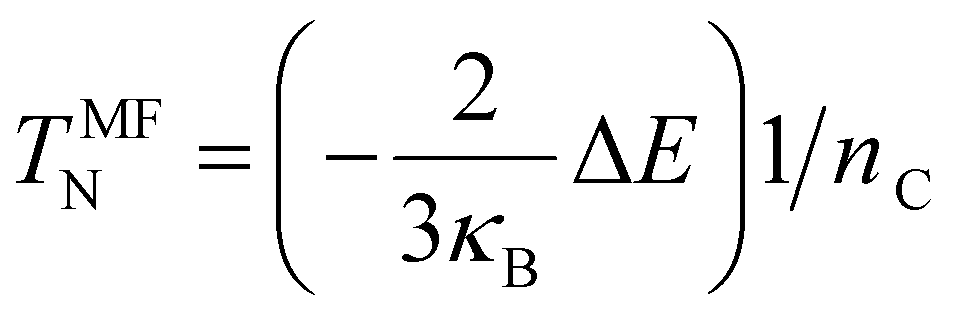
Finally, spin-polarized calculations were also performed and used to estimate the Néel Temperature with the mean-field approximation given by eqn (4):56,57
 | (4) |
4. Conclusions
Energetic, electronic and transport properties of pristine, boron-, and nitrogen-doped 3-triangulene crystals were assessed by a combination of DFT and NEGF methods. Different concentrations of dopants were considered and our results reveal that the formation energies of all doped systems are governed by an exothermic process and scale linearly in energy with the doping concentration. From the structural characterization of the systems, simulated STM images clearly show that doped systems can be distinguished from the pristine one. From an electronic point of view, the band dispersion around the Fermi level can be controlled by the doping and concentration type. For the highest concentration, transmission curves shift toward higher (lower) energies for B (N) doping, and the number of transmission channels at the Fermi level increases with respect to the pristine system. Triangulene kagome lattices’ unique electronic properties and the feasibility of manipulating them through doping make this system a promising candidate for use in next-generation nano-sized bio sensors.Conflicts of interest
There are no conflicts to declare.Acknowledgements
The authors acknowledge the financial support from the Brazilian agencies CAPES, CNPq, and FAPES (TO – 1043/2022) and the computational resources of CENAPAD-SP. WLS and RGA thank CNPq for the financial support (301648/2017-4 and 421227/2018-4; and (2535/2017-1, 437182/2018-5 and 313076/2020-0, respectively). RGA also acknowledges the financial support from FAPERJ, grant numbers E-26/010.101126/2018, E-26/210.077/2022 and E-26/202.699/2019. This study was financed in part by the Coordenação de Aperfeiçoamento de Pessoal de Nível Superior – Brasil (CAPES) – Finance Code 001.References
- K. S. Novoselov, A. K. Geim, S. V. Morozov, D.-e. Jiang, Y. Zhang, S. V. Dubonos, I. V. Grigorieva and A. A. Firsov, Science, 2004, 306, 666–669 CrossRef CAS PubMed.
- A. Casanova, R. Rincón, J. Muñoz, C. Ania and M. Calzada, Fuel Process. Technol., 2021, 212, 106630 CrossRef CAS.
- N. Pavliček, A. Mistry, Z. Majzik, N. Moll, G. Meyer, D. J. Fox and L. Gross, Nat. Nanotechnol., 2017, 12, 308–311 CrossRef PubMed.
- S. Mishra, K. Xu, K. Eimre, H. Komber, J. Ma, C. A. Pignedoli, R. Fasel, X. Feng and P. Ruffieux, Nanoscale, 2021, 13, 1624–1628 RSC.
- J. Su, M. Telychko, P. Hu, G. Macam, P. Mutombo, H. Zhang, Y. Bao, F. Cheng, Z.-Q. Huang and Z. Qiu, et al. , Sci. Adv., 2019, 5, eaav7717 CrossRef CAS PubMed.
- S. Mishra, D. Beyer, K. Eimre, J. Liu, R. Berger, O. Groning, C. A. Pignedoli, K. Mullen, R. Fasel and X. Feng, et al. , J. Am. Chem. Soc., 2019, 141, 10621–10625 CrossRef CAS PubMed.
- S. Mishra, D. Beyer, K. Eimre, R. Ortiz, J. Fernández-Rossier, R. Berger, O. Gröning, C. A. Pignedoli, R. Fasel and X. Feng, et al. , Angew. Chem., 2020, 132, 12139–12145 CrossRef.
- S. Mishra, G. Catarina, F. Wu, R. Ortiz, D. Jacob, K. Eimre, J. Ma, C. A. Pignedoli, X. Feng and P. Ruffieux, et al. , Nature, 2021, 598, 287–292 CrossRef CAS PubMed.
- J. Hieulle, S. Castro, N. Friedrich, A. Vegliante, F. R. Lara, S. Sanz, D. Rey, M. Corso, T. Frederiksen and J. I. Pascual, et al. , Angew. Chem., Int. Ed., 2021, 60, 25224–25229 CrossRef CAS PubMed.
- G. Allinson, R. J. Bushby, J. L. Paillaud, D. Oduwole and K. Sales, J. Am. Chem. Soc., 1993, 115, 2062–2064 CrossRef CAS.
- G. Allison, R. J. Bushby, M. V. Jesudason, J. L. Paillaud and N. Taylor, J. Chem. Soc., Perkin Trans. 2, 1997, 147–156 RSC.
- Y. Jing and T. Heine, J. Am. Chem. Soc., 2018, 141, 743–747 CrossRef PubMed.
- T. Li and Y. Jing, J. Phys. Chem. C, 2022, 126, 17836–17843 CrossRef CAS.
- E. Kan, W. Hu, C. Xiao, R. Lu, K. Deng, J. Yang and H. Su, J. Am. Chem. Soc., 2012, 134, 5718–5721 CrossRef CAS PubMed.
- X. Chen, D. Tan, J. Dong, T. Ma, Y. Duan and D.-T. Yang, J. Phys. Chem. Lett., 2022, 13, 10085–10091 CrossRef CAS PubMed.
- M. Bieri, S. Blankenburg, M. Kivala, C. A. Pignedoli, P. Ruffieux, K. Müllen and R. Fasel, Chem. Commun., 2011, 47, 10239–10241 RSC.
- F. Schlutter, F. Rossel, M. Kivala, V. Enkelmann, J.-P. Gisselbrecht, P. Ruffieux, R. Fasel and K. Mullen, J. Am. Chem. Soc., 2013, 135, 4550–4557 CrossRef PubMed.
- C. Steiner, J. Gebhardt, M. Ammon, Z. Yang, A. Heidenreich, N. Hammer, A. Görling, M. Kivala and S. Maier, Nat. Commun., 2017, 8, 14765 CrossRef CAS PubMed.
- G. Galeotti, F. De Marchi, E. Hamzehpoor, O. MacLean, M. Rajeswara Rao, Y. Chen, L. Besteiro, D. Dettmann, L. Ferrari and F. Frezza, et al. , Nat. Mater., 2020, 19, 874–880 CrossRef CAS PubMed.
- Y. Jing, Z. Zhou, W. Geng, X. Zhu and T. Heine, Adv. Mater., 2021, 33, 2008645 CrossRef CAS PubMed.
- K. N. Anindya and A. Rochefort, Carbon Trends, 2022, 7, 100170 CrossRef CAS.
- R. Ortiz, G. Catarina and J. Fernández-Rossier, 2D Mater., 2022, 10, 015015 CrossRef.
- L. Xue, H. Yamazaki, R. Ren, M. Wanunu, A. P. Ivanov and J. B. Edel, Nat. Rev. Mater., 2020, 5, 931–951 CrossRef CAS.
- J. Prasongkit, E. de Freitas Martins, F. A. De Souza, W. L. Scopel, R. G. Amorim, V. Amornkitbamrung, A. R. Rocha and R. H. Scheicher, J. Phys. Chem. C, 2018, 122, 7094–7099 CrossRef CAS.
- F. A. de Souza, R. G. Amorim, W. L. Scopel and R. H. Scheicher, Phys. Chem. Chem. Phys., 2019, 21, 24884–24890 RSC.
- A. Raza, J. Z. Hassan, A. Mahmood, W. Nabgan and M. Ikram, Desalination, 2022, 531, 115684 CrossRef CAS.
- Z. Cao, V. Liu and A. B. Farimani, Nano Lett., 2019, 19, 8638–8643 CrossRef CAS PubMed.
- G.-R. Xu, J.-M. Xu, H.-C. Su, X.-Y. Liu, H.-L. Zhao, H.-J. Feng and R. Das, et al. , Desalination, 2019, 451, 18–34 CrossRef CAS.
- K. Su, W. Wang, S. Du, C. Ji and D. Yuan, Nat. Commun., 2021, 12, 3703 CrossRef CAS PubMed.
- Y. Yang, L. Li, R.-B. Lin, Y. Ye, Z. Yao, L. Yang, F. Xiang, S. Chen, Z. Zhang and S. Xiang, et al. , Nat. Chem., 2021, 13, 933–939 CrossRef CAS PubMed.
- S. Rashidi, J. A. Esfahani and A. Rashidi, Renewable Sustainable Energy Rev., 2017, 73, 1198–1210 CrossRef CAS.
- S. Zhang, P. Zhang, A. Xie, S. Li, F. Huang and Y. Shen, Electrochim. Acta, 2016, 212, 912–920 CrossRef CAS.
- P. Hohenberg and W. Kohn, Phys. Rev., 1964, 136, B864 CrossRef.
- W. Kohn and L. J. Sham, Phys. Rev., 1965, 140, A1133 CrossRef.
- J. P. Perdew, K. Burke and M. Ernzerhof, Phys. Rev. Lett., 1996, 77, 3865 CrossRef CAS PubMed.
- P. Giannozzi, S. Baroni, N. Bonini, M. Calandra, R. Car, C. Cavazzoni, D. Ceresoli, G. L. Chiarotti, M. Cococcioni and I. Dabo, et al. , J. Phys.: Condens. Matter, 2009, 21, 395502 CrossRef PubMed.
- P. Giannozzi, O. Andreussi, T. Brumme, O. Bunau, M. B. Nardelli, M. Calandra, R. Car, C. Cavazzoni, D. Ceresoli and M. Cococcioni, et al. , J. Phys.: Condens.Matter, 2017, 29, 465901 CrossRef CAS PubMed.
- P. E. Blöchl, Phys. Rev. B: Condens. Matter Mater. Phys., 1994, 50, 17953 CrossRef PubMed.
- J. J. Mortensen, L. B. Hansen and K. W. Jacobsen, Phys. Rev. B: Condens. Matter Mater. Phys., 2005, 71, 035109 CrossRef.
- H. J. Monkhorst and J. D. Pack, Phys. Rev. B: Solid State, 1976, 13, 5188 CrossRef.
- J. M. Soler, E. Artacho, J. D. Gale, A. García, J. Junquera, P. Ordejón and D. Sánchez-Portal, J. Phys.: Condens. Matter, 2002, 14, 2745 CrossRef CAS.
- A. García, N. Papior, A. Akhtar, E. Artacho, V. Blum, E. Bosoni, P. Brandimarte, M. Brandbyge, J. I. Cerdá and F. Corsetti, et al. , J. Chem. Phys., 2020, 152, 204108 CrossRef PubMed.
- D. Hamann, M. Schlüter and C. Chiang, Phys. Rev. Lett., 1979, 43, 1494 CrossRef CAS.
- J. Junquera, Ó. Paz, D. Sánchez-Portal and E. Artacho, Phys. Rev. B: Condens. Matter Mater. Phys., 2001, 64, 235111 CrossRef.
- J. Tersoff and D. R. Hamann, Phys. Rev. B: Condens. Matter Mater. Phys., 1985, 31, 805 CrossRef CAS PubMed.
- M. Brandbyge, J.-L. Mozos, P. Ordejón, J. Taylor and K. Stokbro, Phys. Rev. B: Condens. Matter Mater. Phys., 2002, 65, 165401 CrossRef.
- N. Papior, N. Lorente, T. Frederiksen, A. García and M. Brandbyge, Comput. Phys. Commun., 2017, 212, 8–24 CrossRef CAS.
- T. Wang, A. Berdonces-Layunta, N. Friedrich, M. Vilas-Varela, J. P. Calupitan, J. I. Pascual, D. Pena, D. Casanova, M. Corso and D. G. de Oteyza, J. Am. Chem. Soc., 2022, 144, 4522–4529 CrossRef CAS PubMed.
- S. Su, X. Wang and J. Xue, Mater. Horiz., 2021, 8, 1390–1408 RSC.
- T. M. Dieb, Z. Hou and K. Tsuda, J. Chem. Phys., 2018, 148, 241716 CrossRef PubMed.
- M. Yang, L. Wang, M. Li, T. Hou and Y. Li, AIP Adv., 2015, 5, 067136 CrossRef.
- P. Rani and V. Jindal, RSC Adv., 2013, 3, 802–812 RSC.
- H. I. Sirikumara, E. Putz, M. Al-Abboodi and T. Jayasekera, Sci. Rep., 2016, 6, 19115 CrossRef CAS PubMed.
- G. Henkelman, A. Arnaldsson and H. Jónsson, Comput. Mater. Sci., 2006, 36, 354–360 CrossRef.
- W. Tang, E. Sanville and G. Henkelman, J. Phys.: Condens. Matter, 2009, 21, 084204 CrossRef CAS PubMed.
- H. Shi, H. Pan, Y.-W. Zhang and B. I. Yakobson, Phys. Rev. B: Condens. Matter Mater. Phys., 2013, 88, 205305 CrossRef.
- P. D. Reyntjens, S. Tiwari, M. L. Van de Put, B. Soree and W. G. Vandenberghe, 2D Mater., 2020, 8, 025009 CrossRef.
Footnote |
| † Electronic supplementary information (ESI) available. See DOI: https://doi.org/10.1039/d4nr00910j |
| This journal is © The Royal Society of Chemistry 2024 |