
 Open Access Article
 This Open Access Article is licensed under a Creative Commons Attribution-Non Commercial 3.0 Unported Licence
Structural alignment of ZnO columns across multiple monolayer MoS2 layers as compliant substrates†
Xuejing
Wang
a,
Kyungtae
Kim
 a,
Benjamin K.
Derby
a,
Terrence
McGuckin
b,
Gabriel A.
Calderón
c,
Michael T.
Pettes
a,
Jinwoo
Hwang
c,
Yeonhoo
Kim
d,
Jeongwon
Park
e,
Aiping
Chen
a,
Kibum
Kang
e and
Jinkyoung
Yoo
*a
a,
Benjamin K.
Derby
a,
Terrence
McGuckin
b,
Gabriel A.
Calderón
c,
Michael T.
Pettes
a,
Jinwoo
Hwang
c,
Yeonhoo
Kim
d,
Jeongwon
Park
e,
Aiping
Chen
a,
Kibum
Kang
e and
Jinkyoung
Yoo
*a
aCenter for Integrated Nanotechnologies, Los Alamos National Laboratory, Los Alamos, NM 87545, USA. E-mail: jyoo@lanl.gov
bEphemeron-Labs, Inc., Philadelphia, PA 19134, USA
cDepartment of Materials Science and Engineering, The Ohio State University, Columbus, OH 43210, USA
dInterdisciplinary Materials Measurement Institute, Korea Research Institute of Standards and Science, Daejeon 34133, Republic of Korea
eDepartment of Materials Science and Engineering, Korea Advanced Institute of Science and Technology (KAIST), 291 Daehak-ro, Yuseong-gu, Daejeon 34141, Republic of Korea
First published on 1st April 2024
Abstract
Understanding the behavior of materials in multi-dimensional architectures composed of atomically thin two-dimensional (2D) materials and three-dimensional (3D) materials has become mandatory for progress in materials preparation via various epitaxy techniques, such as van der Waals and remote epitaxy methods. We investigated the growth behavior of ZnO on monolayer MoS2 as a model system to study the growth of a 3D material on a 2D material, which is beyond the scope of remote and van der Waals epitaxy. The study revealed column-to-column alignment and inversion of crystallinity, which can be explained by combinatorial epitaxy, grain alignment across an atomically sharp interface, and a compliant substrate. The growth study enabled the formation of a ZnO/MoS2 heterostructure with type-I band alignment. Our findings will have a scientific impact on realizing 2D/3D heterostructures for practical device applications.
Introduction
Multi-dimensional architectures composed of atomically thin two-dimensional (2D) materials and three-dimensional (3D) materials, such as thin films and bulk materials, have attracted a lot of attention with respect to overcoming material compatibility and the ability to deliver novel functionality.1–3 Conventional thin films such as complex oxides and III–V nitrides, which possess controllable intrinsic characteristics and surface properties, serve as ideal candidates to couple with 2D layers to create robust functional heterostructures.4–8 There have been numerous studies of 2D/3D integration, in which remote and van der Waals (vdW) epitaxy techniques are used to create high-quality semiconductor films that are transferrable, to realize reusable substrates; the proximity effect can be used to manipulate the properties of 2D materials, such as those coupled with high-temperature magnetic thin films or superconductors for practical transistor development in which conventional gate oxides are replaced by these novel 2D components.2,9,10 These research efforts offer tremendous opportunities, beyond traditional bulky device designs, to reveal new physical functionalities that exceed the inherent limits of materials. However, remote and vdW epitaxy studies represent only some of the scientific topics on 2D/3D heterogeneous integration because epitaxy-based approaches still require consideration of the crystal structures of individual components and interfacial coupling to make vdW interaction and field penetration dominant.Epitaxy research encompasses broad aspects of material combination beyond matching the crystal structures and thermal coefficients. In conventional 3D/3D heterostructures prepared by epitaxy techniques, some studies have focused on epitaxial behavior on polycrystalline substrates (combinatorial epitaxy) and unconventional substrates in which the strain is relaxed either through the substrate or through the grown layer (a compliant substrate).11–16 As 2D materials are being employed as substrates for the growth of 3D materials, studies covering the effects of substrates on material growth have become necessary. The interactions between the grown 3D material and 2D substrate are diverse, beyond those of lattice transparency and enhanced atom slip.8,17,18
The growth of a crystalline 3D material on a 2D substrate has two characteristics of combinatorial epitaxy and compliant substrate, as most 2D materials are polycrystalline thin films, and the volume of the 2D material is significantly less than that of the grown 3D material. Insights obtained by studying 3D material growth on a 2D material implementing combinatorial epitaxy on a compliant substrate will be applicable to common cases of 2D/3D heterogeneous integration.
To probe the interfacial structure and properties between semiconductor thin films and atomically thin vdW layers, we prepared a five-layer heterostructure stack composed of ZnO/MoS2/ZnO/MoS2/ZnO layers. We highlight two aspects of our achievements in this work as follows: (i) Random in-plane ordering with preservation of columnar growth across the monolayer (1L)-MoS2 layers; here, we show the existence of 1L-MoS2 as well as an improvement in the crystallinity of ZnO growth at the top layer, as confirmed by high-resolution transmission electron microscopy (HRTEM) and scanning TEM (STEM), X-ray diffraction (XRD), photoluminescence (PL), and Raman measurements. (ii) Compared to the wide bandgap of ZnO, monolayer MoS2 with a narrower bandgap serves as a sink for charge carriers; interfacial charge transport properties were explored using electron beam absorbed current (EBAC) measurements. Overall, the growth of complex heterostructures obtained by stacking 2D and 3D components is of great importance to fundamental material science with a view to the development of highly functional optoelectronic devices.
Methods
Growth of ZnO film by pulsed laser deposition (PLD)
ZnO layers were grown using a PLD system. The base pressure was 5 × 10⁻⁶ Torr. Epitaxial ZnO thin films were grown on c-Al2O3 substrates at 600 °C under an oxygen partial pressure of 200 mTorr with a laser frequency of 5 Hz. The ZnO layers on transferred monolayer (1L)-MoS2 films were grown at 200 °C under an oxygen partial pressure of 10 mTorr for the first 50 laser pulses followed by growth under an oxygen partial pressure of 200 mTorr. After the growth, the sample was cooled at a speed of 5–10 °C min−1.Transfer of 1L-MoS2
1L-MoS2 thin film was grown on an SiO2/Si substrate by metalorganic chemical vapor deposition. Details of 1L-MoS2 are described elsewhere.19,20 Poly(methyl)methacrylate (PMMA, MicroChem® 495K A4) was coated on the 1L-MoS2 thin film by spin coating. The PMMA-coated 1L-MoS2 thin film was separated by etching an SiO2 layer in potassium hydroxide aqueous solution. The floating PMMA-coated 1L-MoS2 was moved to deionized water. Subsequently, the PMMA/1L-MoS2 membrane was transferred onto a ZnO layer. The PMMA/1L-MoS2/ZnO was dried at 70 °C for 8 h on a hot plate. The PMMA layer was removed in acetone.Structural characterization
Cross-sectional TEM (X-TEM) samples were prepared by a mechanical polishing and dimpling process. The <30 μm-thin sample was milled by argon (Ar) ion milling (Gatan PIPS II 65) with a beam energy of 3.7 keV. Scanning TEM (STEM), bright field TEM, and energy dispersive X-ray (EDX) characterization were performed on X-TEM samples. XRD θ–2θ scans were performed on a Rigaku SmartLab II diffractometer. Grazing incidence wide angle X-ray scattering (GIWAXS) was performed to investigate the in-plane ordering of the topmost ZnO layer of the ZnO/1L-MoS2/ZnO/1L-MoS2/ZnO/c-Al2O3 sample. Two-dimensional scattering patterns were acquired using a XEUSS 3.0 small/wide angle scattering system equipped with a Cu Kα X-ray source (λ = 1.5407 Å) at an incident angle of 0.14° and sample-to-detector distance of 72 mm.PL and Raman spectroscopy
PL and Raman spectroscopic measurements were conducted at room temperature using 244 nm (100% = 21.8 μW) and 633 nm (100% = 10 mW) wave excitation, respectively, in a Horiba LabRAM HR Evolution high resolution confocal PL/Raman microscope fitted with volume Bragg gratings. Grating was calibrated with an Hg (Ar) spectral calibration lamp. Spectral calibration was performed using the 1332.5 cm−1 band of a synthetic Type IIa diamond, and spectral intensity was calibrated using a VIS-halogen light source (488–633 nm laser lines).EBAC microscopy
Carrier diffusion lengths across the ZnO layers separated by 1L-MoS2 layers were measured by EBAC measurements with a low-noise EBAC system (Mighty EBIC, Ephemeron-Labs, Inc.) installed on an SEM. All measurements were conducted in a direct current configuration. The substrate was held at ground. The electron beam current and acceleration voltage were ∼100 pA and 10 kV, respectively.Results and discussion
To study the effects of 1L-MoS2 on ZnO growth, preservation of 1L-MoS2 after ZnO deposition was confirmed by PL and Raman measurements. Fig. 1(a) shows a schematic diagram of a ZnO/1L-MoS2/ZnO stack to show the 1L-MoS2 layer surrounded with ZnO films deposited by PLD. Fig. 1(b) shows PL spectra at room temperature, taken at four random spots (P1–P4) on the ZnO/1L-MoS2/ZnO stack. The strong near-band edge emission (NBE) peak of ZnO was observed at 378.6 nm.21 The inset of Fig. 1 shows the PL spectra over the range of 450–700 nm; the visible emission originated from the oxygen vacancies of ZnO (shown in cyan) and from excitons of 1L-MoS2 (shown in pink).22–24 Raman spectra are displayed in Fig. 1(c), collected at another four random spots (P5–P8) on the ZnO/1L-MoS2/ZnO stack. For comparison, we noticed that P5 and P6 could be edge positions of the sample that only contains ZnO, with its two major phonon modes, a sharp Ehigh2 mode at 436 cm−1, and a weak Ehigh2–Elow2 mode at 333 cm−1 being detected.25 At P7 and P8, MoS2 and ZnO modes were observed, such as 2LA at 450 cm−1, A1g at 413 cm−1 and E2g1 at 375 cm−1 that match those of 1L-MoS2. Observation of characteristic optical responses from 1L-MoS2 surrounded by 3D materials has rarely been reported under mild conditions (e.g., a growth temperature of 90 °C)8 or with significant quenching of the PL emission of MoS2.26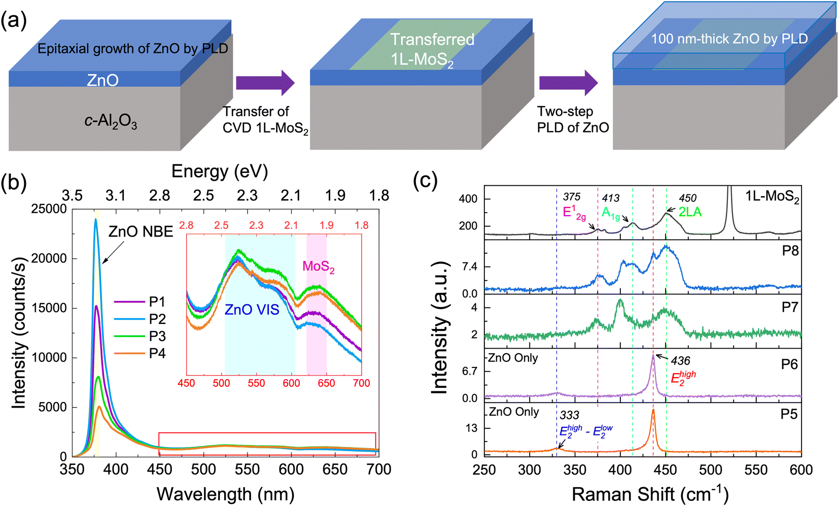 | ||
| Fig. 1 (a) Schematic of ZnO/1L-MoS2/ZnO preparation by transfer of MoS2 and PLD of ZnO. (b) PL spectra collected at four different spots (P1–P4) of the ZnO/MoS2 5-layer stack. The inset displays the zoomed view at 450–700 nm range. (c) Raman spectra collected at four different positions (P5–P8) of the ZnO/1L-MoS2/ZnO stack with the as-grown 1L-MoS2 on SiO2/Si as reference (black). The spectra at P5 and P6 and those at P7 and P8 were obtained from the regions of ZnO only and regions of the ZnO/1L-MoS2/ZnO stack, respectively. | ||
After confirmation of the preservation of 1L-MoS2 after ZnO growth, a multi-layer stack composed of ZnO and the 1L-MoS2 layers, as depicted in Fig. 2(a), was fabricated to study structural changes with the repetition of 2D and 3D layer preparation. We name the three ZnO layers as L1 (bottom, on c-Al2O3), L2 (middle, on the first 1L-MoS2) and L3 (top, on the second 1L-MoS2) to differentiate their growth and crystallinity. Two MOCVD-grown 1L-MoS2 continuous thin films (5 mm × 5 mm) were wet transferred. The first and second transfers were performed on L1 and L2 ZnO, respectively. Two 1L-MoS2 layers were clearly identified in cross-sectional high-angle annular dark field (HAADF) STEM (Fig. 2(a)). However, we also noticed that additional exposure of the same sample under the electron beam at an acceleration voltage of 300 kV caused radiation damage to MoS2 layers, which were observed as a dark void-like morphology in the area. From the XRD θ–2θ (Fig. 2(b)), the as-grown ZnO layer (black) shows the desired epitaxial quality dominated by its (002) peak at 34.54°. Surface smoothness can be further improved by enhancing recipes for ZnO L1. This potentially indicates that the growth of ZnO at L2 and L3 is aligned with columns. A detailed XRD θ–2θ scan of the 5-layer ZnO/MoS2 stack showed the dominant ZnO (0002) peak without a noticeable shift, which suggests that all ZnO layers (L1, L2, and L3) are c-axis oriented regardless of inserted 1L-MoS2 layers. We noticed that MoS2 (100), covered by ZnO (0002) at the shoulder peak at 36.1°, can be correlated with the highly strained MoS2 (103) plane,27 providing more evidence of MoS2.
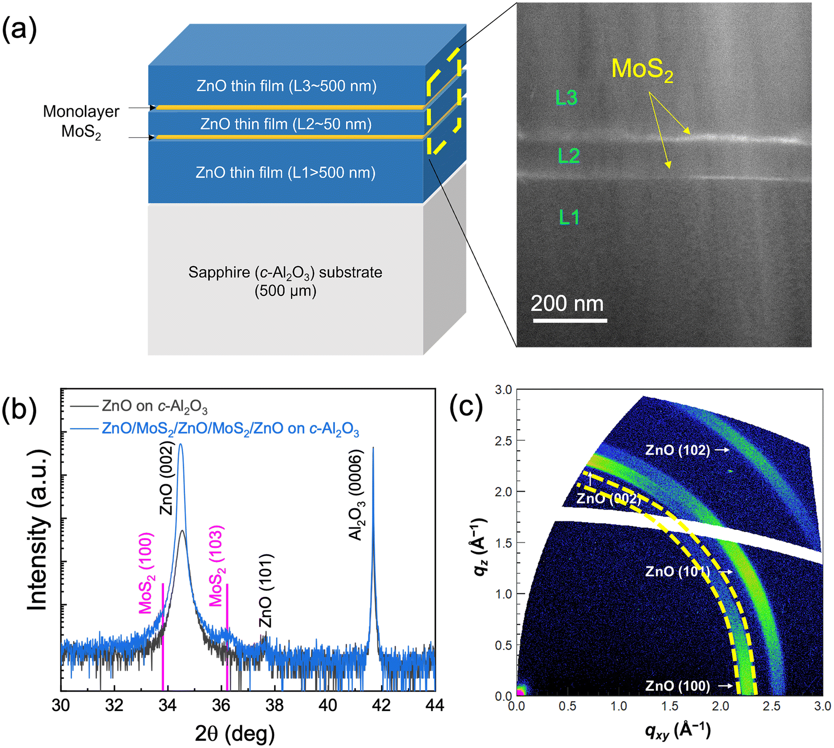 | ||
| Fig. 2 (a) Cross-sectional low-magnification STEM image (first exposure under e-beam). Bright contrast indicates the existence of 1L-MoS2. The inset shows the scheme of the ZnO/MoS2 5-layer stack. (b) XRD θ–2θ scan of the ZnO/MoS2/ZnO/MoS2/ZnO/c-Al2O3 sample. (c) Wedge-corrected GIWAXS image of the topmost ZnO layer (L3) of the ZnO/MoS2/ZnO/MoS2/ZnO/c-Al2O3 sample. | ||
To investigate the in-plane ordering of the ZnO layers in the 5-layer stack, GIWAXS was performed on the topmost ZnO layer (L3), as shown in Fig. 2(c). The intensity distribution of scattering arcs in qxy and qz directions indicates that the c-axes of ZnO crystals align parallel with the directions of column growth. The GIWAXS pattern did not change when the sample specimen was rotated around the axis perpendicular to the surface, which means that there is no specific in-plane ordering. The absence of in-plane ordering in ZnO L3 originates from the polycrystalline nature of the in-plane ordering of 1L-MoS2. The alignment of the ZnO layers (L1, L2, and L3) along the out-of-plane direction and without in-plane ordering reveals that the 5 layer-stack is an appropriate platform for studying combinatorial epitaxy implemented on a polycrystalline substrate and structural alignment through an atomically thin substrate.
The out-of-plane alignment and crystallinity of the ZnO layers across the 1L-MoS2 layers was investigated by TEM. A heterostructure stack was revealed under the bright-field (BF) STEM mode (Fig. 3(a)). Fig. 3(a) also shows that the growth of ZnO was governed by a columnar growth mode. The thickness of each ZnO layer was identified as approximately 1.5 μm for L1, 70 nm for L2, and 400 nm for L3. The surface roughness of L1 and L3 is noticeably larger than that of L2 due to an increase in surface roughness along with layer thickness, which is commonly observed for columnar growth. ZnO L1 contained threading dislocations (red arrow), which are displayed as dark line features originating at the beginning of the growth. Notably, threading dislocations are commonly observed in the ZnO films grown on c-Al2O3 due to the large in-plane lattice mismatch of 18.3%.28–30 The structural characteristics of individual L1, L2, and L3 ZnO layers and adjacent interfaces were investigated by TEM, as displayed in Fig. 3. The inset of Fig. 3(a) shows continuous column formations in ZnO L1, L2, and L3 along the out-of-plane direction. Column-to-column alignment has been reported in oxide multi-layers and metal bilayers with atomically sharp interfaces.13,31,32 The observation of columnar growth and continuous formation of the 1L-MoS2 layers indicates that lateral overgrowth was not dominant in the ZnO/MoS2 multi-stack. In conjunction with the absence of in-plane ordering, the column-to-column alignment indicates that the five-layer-ZnO/MoS2 stack follows combinatorial epitaxy behavior. Fig. 3(b), (d), and (f) are the zoomed-in versions of yellow-boxed areas 1, 2, and 3 in Fig. 3(a), respectively. The first interface (Fig. 3(b) and (c)), ZnO L1/c-Al2O3, appeared as a sharp and clean interface with the typical heteroepitaxial matching relationship between 〈0![[1 with combining macron]](https://www.rsc.org/images/entities/char_0031_0304.gif) 11〉 c-Al2O3 and 〈20〉 ZnO zone axes. The corresponding fast-Fourier transform (FFT) in Fig. 1(c) clearly identifies the spots from ZnO and Al2O3. Fig. 3(d) and (e) show that ZnO L2 is strained with a polycrystalline nature, as evidenced by red dashed lines indicating strain contours as well as ring-like FFTs. However, in the imaged area, 〈20〉 ZnO lattices appeared to be aligned without rotation (red bar). Fig. S1a† shows a STEM image of this interface in which ZnO columns were misaligned with an angular deviation of 5.5°. In ZnO L2, the strain was relaxed through column formation, which generated numerous boundaries. Fig. 3(f) and (g) show that ZnO L3 is also polycrystalline. However, the crystallinity of L3 was remarkably improved compared to that of L2. The inversion in the crystallinity trend over the growth sequence can be explained by strain relaxation through thin and polycrystalline 1L-MoS2/ZnO L2. In ZnO L2 and L3, there was no experimental evidence of inversion of polarity of the ionic crystal of ZnO as the previous theoretical calculation indicates.8 Reducing the effective thickness of a substrate creates conditions for strain relaxation in the substrate, resulting in enhanced critical thickness and improved crystallinity.33 The ‘compliant substrate’ concept has been implemented using porous, thin, polycrystalline, and atomically thin substrates,14,16,34,35 corresponding to 1L-MoS2/70 nm-thick ZnO L2. In the aligned columns of ZnO L3, there is no relative rotation between L2 and L3, which is also demonstrated by multiple imaged columns (Fig. S1b†). It is again noted that 1L-MoS2 could be damaged upon extended beam exposure, thus appearing as indiscernible in the TEM mode (Fig. 3(d) and (f)) and in dark contrast in STEM mode (Fig. S1a†). More evidence on the existence of a sharp MoS2 interface is provided by EDX mapping; in Fig. S2,† we can clearly see the gapped lines (dark) of Zn and O as marked in white arrows, which suggests no noticeable intermixing or chemical diffusion between ZnO and MoS2.
11〉 c-Al2O3 and 〈20〉 ZnO zone axes. The corresponding fast-Fourier transform (FFT) in Fig. 1(c) clearly identifies the spots from ZnO and Al2O3. Fig. 3(d) and (e) show that ZnO L2 is strained with a polycrystalline nature, as evidenced by red dashed lines indicating strain contours as well as ring-like FFTs. However, in the imaged area, 〈20〉 ZnO lattices appeared to be aligned without rotation (red bar). Fig. S1a† shows a STEM image of this interface in which ZnO columns were misaligned with an angular deviation of 5.5°. In ZnO L2, the strain was relaxed through column formation, which generated numerous boundaries. Fig. 3(f) and (g) show that ZnO L3 is also polycrystalline. However, the crystallinity of L3 was remarkably improved compared to that of L2. The inversion in the crystallinity trend over the growth sequence can be explained by strain relaxation through thin and polycrystalline 1L-MoS2/ZnO L2. In ZnO L2 and L3, there was no experimental evidence of inversion of polarity of the ionic crystal of ZnO as the previous theoretical calculation indicates.8 Reducing the effective thickness of a substrate creates conditions for strain relaxation in the substrate, resulting in enhanced critical thickness and improved crystallinity.33 The ‘compliant substrate’ concept has been implemented using porous, thin, polycrystalline, and atomically thin substrates,14,16,34,35 corresponding to 1L-MoS2/70 nm-thick ZnO L2. In the aligned columns of ZnO L3, there is no relative rotation between L2 and L3, which is also demonstrated by multiple imaged columns (Fig. S1b†). It is again noted that 1L-MoS2 could be damaged upon extended beam exposure, thus appearing as indiscernible in the TEM mode (Fig. 3(d) and (f)) and in dark contrast in STEM mode (Fig. S1a†). More evidence on the existence of a sharp MoS2 interface is provided by EDX mapping; in Fig. S2,† we can clearly see the gapped lines (dark) of Zn and O as marked in white arrows, which suggests no noticeable intermixing or chemical diffusion between ZnO and MoS2.
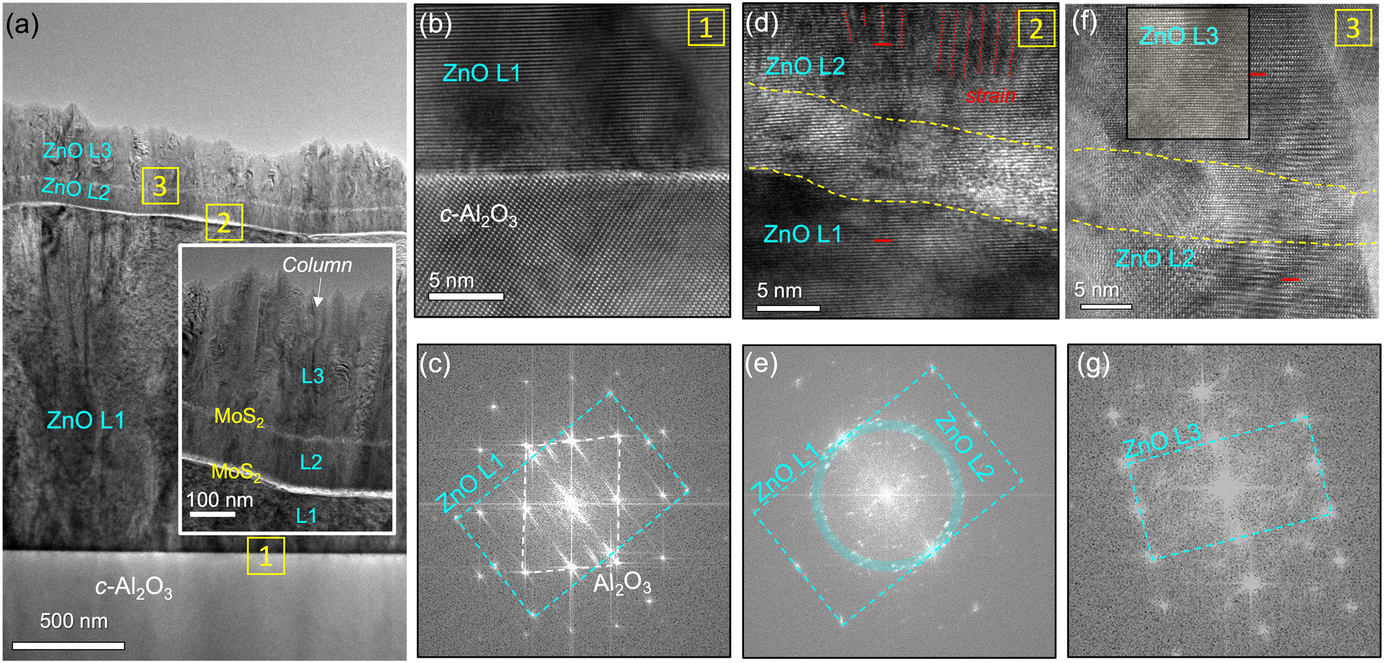 | ||
| Fig. 3 (a) TEM micrograph displaying the entire 5-layer stack on the c-Al2O3 substrate. Areas of interest are marked as squares 1, 2, and 3. HRTEM images at individual (b) ZnO L1/c-Al2O3 interface, (d) ZnO L1/1L-MoS2/ZnO L2 interface, and (f) ZnO L2/1L-MoS2/ZnO L3 interface. (c, e and g) Corresponding FFTs. | ||
The changes in crystallinity in individual ZnO layers affect the physical properties of ZnO. The correlation between crystallinity and electrical characteristics, represented by carrier diffusion length, was investigated by EBAC mapping across all the layers comprising the five-layer stack. Fig. 4(a) shows the EBAC map of the ZnO/1L-MoS2 multilayer stack. The EBAC is strong in the region of 1L-MoS2/ZnO L2/1L-MoS2. The highly concentrated EBAC indicates that injected electrons are funneled into 1L-MoS2/ZnO L2/1L-MoS2. By plotting the current profile (Fig. 4(b)) with respect to the line position marked in Fig. 4(a), the major peak can be divided into four regions according to its variations in slope, marked as colored D1 to D4. The strong absorption of injected carriers (higher EBAC) in the 1L-MoS2/ZnO L2/1L-MoS2 region is explained by the narrow band gap of the MoS2 layers that act as a double-quantum-well with type-I band alignment, as depicted in Fig. 4(b).
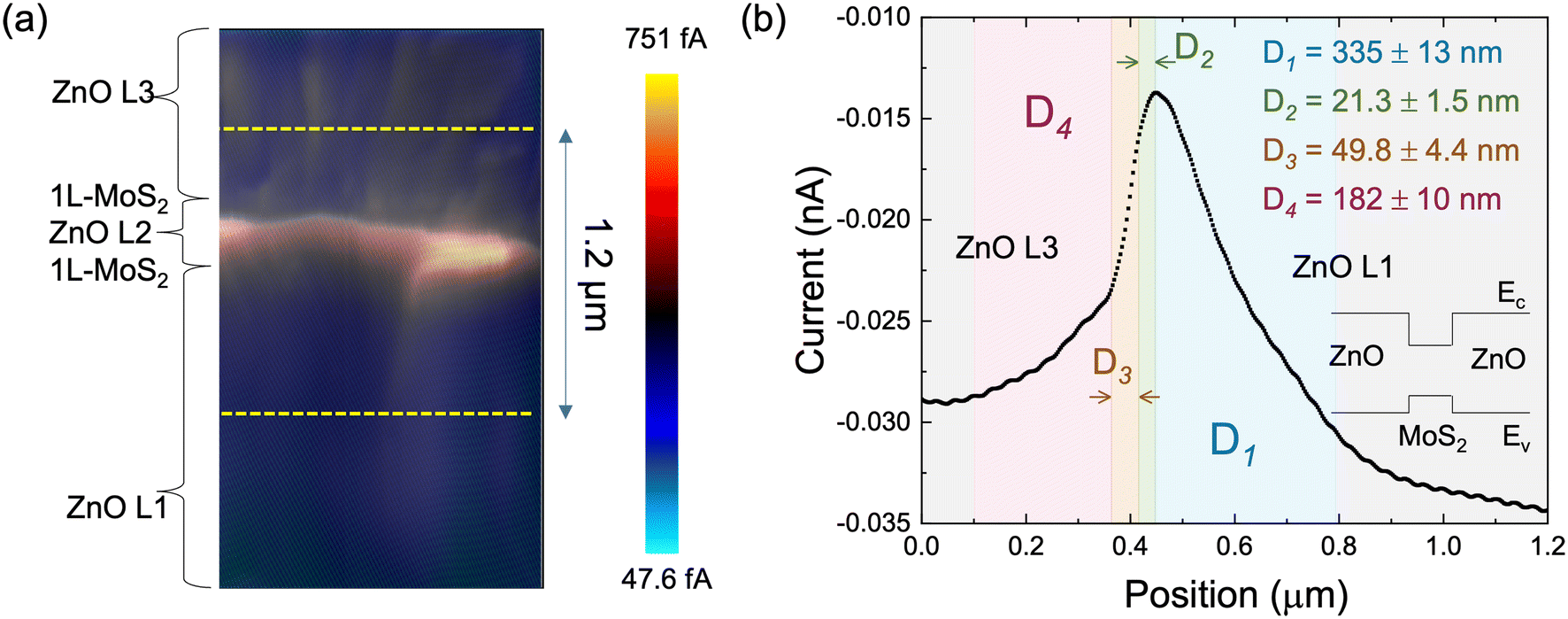 | ||
| Fig. 4 (a) EBAC mapping of the ZnO/1L-MoS2/ZnO/1L-MoS2/ZnO stack. (b) Current distribution curve across the scanned area at the interface. D1–D4 represent calculated current diffusion lengths. The inset is a schematic illustration of the heterojunction and its electronic band profile. | ||
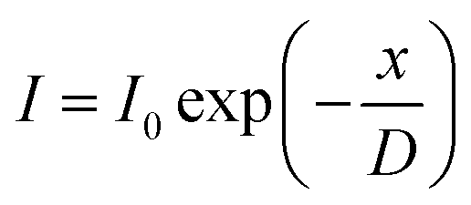
Considering each ZnO layer as a single medium and assuming isotropic electron diffusion in a ZnO layer, the carrier diffusion length can be estimated from EBAC data, as a function of the distance between an electron beam spot and an EBAC peak, as follows:
Conclusions
We designed an architecture composed of multiple ZnO and 1L-MoS2 layers to study the growth behaviors of a 2D/3D heterostructure using means other than remote and vdW epitaxy. Microscopic analysis at the atomic scale indicated clean interfaces at each of ZnO/1L-MoS2. ZnO L1 on a crystalline c-Al2O3 showed conventional epitaxy behavior. Meanwhile, ZnO L2 and L3 grown on 1L-MoS2 layers showed column-to-column alignment and inversion of the crystallinity along the growth direction, which can be explained by combinatorial epitaxy with a compliant substrate. The crystallinity of individual ZnO layers correlated with specific carrier diffusion lengths, as estimated by EBAC. The heterojunction of ZnO/1L-MoS2/ZnO/1L-MoS2/ZnO showed a highly concentrated EBAC that could be of great importance to the design of complex optoelectronic heterostructures. Fundamentally, this study provides insight into the 2D/3D heterostructure, its associated interfaces, and techniques to evaluate various layers, to facilitate the realization of other material systems using similar methods.Author contributions
J.Y. conceived and directed the main experimental idea; X.W. and A.C. performed ZnO deposition; X.W., B.K.D., G.A.C., and J.H. performed X-TEM sample preparation, HRTEM, and STEM. M.P. conducted Raman mapping and analyses with X.W.; T.M. conducted EBAC measurements and analyses with J.Y.; Y.K. and J.Y. performed MoS2 transfer; J.P. and K.K. prepared monolayer MoS2 thin films; J.Y. is responsible for all research results. X.W. and J.Y. co-wrote the manuscript. All authors discussed and commented on the manuscript.Conflicts of interest
There are no conflicts to declare.Acknowledgements
This research was financially supported by the Laboratory Directed Research and Development Program of Los Alamos National Laboratory (20190224ER). This work was partly performed at CINT, a U.S. Department of Energy, office of Basic Energy Sciences User Facility at Los Alamos National Laboratory (Contract 89233218CNA000001) and Sandia National Laboratories (Contract DE-NA-0003525). G. A. C. and J. H. acknowledge funding support by the National Science Foundation under DMR-2011876.References
- D. Jariwala, T. J. Marks and M. C. Hersam, Nat. Mater., 2017, 16, 170–181 CrossRef CAS PubMed.
- S.-H. Bae, H. Kum, W. Kong, Y. Kim, C. Choi, B. Lee, P. Lin, Y. Park and J. Kim, Nat. Mater., 2019, 18, 550–560 CrossRef CAS PubMed.
- P.-Y. Huang, J.-K. Qin, C.-Y. Zhu, L. Zhen and C.-Y. Xu, J. Phys.: Condens. Matter, 2021, 33, 493001 CrossRef CAS PubMed.
- Y. Feng, X. Yang, Z. Zhang, D. Kang, J. Zhang, K. Liu, X. Li, J. Shen, F. Liu, T. Wang, P. Ji, F. Xu, N. Tang, T. Yu, X. Wang, D. Yu, W. Ge and B. Shen, Adv. Funct. Mater., 2019, 29, 1905056 CrossRef CAS.
- T. Ayari, S. Sundaram, C. Bishop, A. Mballo, P. Vuong, Y. Halfaya, S. Karrakchou, S. Gautier, P. L. Voss, J. P. Salvestrini and A. Ougazzaden, Adv. Mater. Technol., 2019, 4, 1900164 CrossRef CAS.
- J. Yu, L. Wang, Z. Hao, Y. Luo, C. Sun, J. Wang, Y. Han, B. Xiong and H. Li, Adv. Mater., 2020, 32, 1903407 CrossRef CAS.
- J. Jeong, Q. Wang, J. Cha, D. K. Jin, D. H. Shin, S. Kwon, B. K. Kang, J. H. Jang, W. S. Yang, Y. S. Choi, J. Yoo, J. K. Kim, C.-H. Lee, S. W. Lee, A. Zakhidov, S. Hong, M. J. Kim and Y. J. Hong, Sci. Adv., 2020, 6, eaaz5180 CrossRef CAS.
- Y. Kim, J. Watt, X. Ma, T. Ahmed, S. Kim, K. Kang, T. S. Luk, Y. J. Hong and J. Yoo, ACS Nano, 2022, 16, 2399–2406 CrossRef CAS PubMed.
- S. Chae, S. Jang, W. J. Choi, Y. S. Kim, H. Chang, T. I. Lee and J.-O. Lee, Nano Lett., 2017, 17, 1711–1718 CrossRef CAS.
- Y. Kim, S. S. Cruz, K. Lee, B. O. Alawode, C. Choi, Y. Song, J. M. Johnson, C. Heidelberger, W. Kong, S. Choi, K. Qiao, I. Almansouri, E. A. Fitzgerald, J. Kong, A. M. Kolpak, J. Hwang and J. Kim, Nature, 2017, 544, 340–343 CrossRef CAS PubMed.
- Y. Zhang, A. M. Schultz, L. Li, H. Chien, P. A. Salvador and G. S. Rohrer, Acta Mater., 2012, 60, 6486–6493 CrossRef CAS.
- S. Havelia, S. Wang, K. R. Balasubramaniam, A. M. Schultz, G. S. Rohrer and P. A. Salvador, CrystEngComm, 2013, 15, 5434–5441 RSC.
- D. Pravarthana, M. Trassin, J. Haw Chu, M. Lacotte, A. David, R. Ramesh, P. A. Salvador and W. Prellier, Appl. Phys. Lett., 2014, 104, 082914 CrossRef.
- Y. Zhou, D. Kiriya, E. E. Haller, J. W. Ager, A. Javey and D. C. Chrzan, Phys. Rev. B, 2016, 93, 054106 CrossRef.
- S. Keller, S. S. Pasayat, C. Gupta, S. P. DenBaars, S. Nakamura and U. K. Mishra, Phys. Status Solidi RRL, 2021, 15, 2100234 CrossRef CAS.
- A. Heintz, B. Ilahi, A. Pofelski, G. Botton, G. Patriarche, A. Barzaghi, S. Fafard, R. Arès, G. Isella and A. Boucherif, Nat. Commun., 2022, 13, 6624 CrossRef CAS.
- K. Reidy, J. D. Thomsen, H. Y. Lee, V. Zarubin, Y. Yu, B. Wang, T. Pham, P. Periwal and F. M. Ross, Nano Lett., 2022, 22, 5849–5858 CrossRef CAS PubMed.
- K. Reidy, P. E. Majchrzak, B. Haas, J. D. Thomsen, A. Konečná, E. Park, J. Klein, A. J. H. Jones, K. Volckaert, D. Biswas, M. D. Watson, C. Cacho, P. Narang, C. T. Koch, S. Ulstrup, F. M. Ross and J. C. Idrobo, Nano Lett., 2023, 23, 1068–1076 CrossRef CAS PubMed.
- K. Kang, S. Xie, L. Huang, Y. Han, P. Y. Huang, K. F. Mak, C.-J. Kim, D. Muller and J. Park, Nature, 2015, 520, 656–660 CrossRef CAS PubMed.
- T. S. Kim, K. P. Dhakal, E. Park, G. Noh, H.-J. Chai, Y. Kim, S. Oh, M. Kang, J. Park, J. Kim, S. Kim, H. Y. Jeong, S. Bang, J. Y. Kwak, J. Kim and K. Kang, Small, 2022, 18, 2106368 CrossRef CAS PubMed.
- B. K. Meyer, H. Alves, D. M. Hofmann, W. Kriegseis, D. Forster, F. Bertram, J. Christen, A. Hoffmann, M. Straßburg, M. Dworzak, U. Haboeck and A. V. Rodina, Phys. Status Solidi B, 2004, 241, 231–260 CrossRef CAS.
- G. Eda, H. Yamaguchi, D. Voiry, T. Fujita, M. Chen and M. Chhowalla, Nano Lett., 2011, 11, 5111–5116 CrossRef CAS PubMed.
- D. Kaplan, Y. Gong, K. Mills, V. Swaminathan, P. M. Ajayan, S. Shirodkar and E. Kaxiras, 2D Mater., 2016, 3, 015005 CrossRef.
- B. Lin, Z. Fu and Y. Jia, Appl. Phys. Lett., 2001, 79, 943–945 CrossRef CAS.
- R. Cuscó, E. Alarcón-Lladó, J. Ibáñez, L. Artús, J. Jiménez, B. Wang and M. J. Callahan, Phys. Rev. B: Condens. Matter Mater. Phys., 2007, 75, 165202 CrossRef.
- C.-H. Ma, L.-S. Lu, H. Song, J.-W. Chen, P.-C. Wu, C.-L. Wu, R. Huang, W.-H. Chang and Y.-H. Chu, APL Mater., 2021, 9, 051115 CrossRef CAS.
- P. Joensen, E. D. Crozier, N. Alberding and R. F. Frindt, J. Phys. C: Solid State Phys., 1987, 20, 4043 CrossRef CAS.
- Y. Chen, D. M. Bagnall, H.-j. Koh, K.-t. Park, K. Hiraga, Z. Zhu and T. Yao, J. Appl. Phys., 1998, 84, 3912–3918 CrossRef CAS.
- S. I. Park, T. S. Cho, S. J. Doh, J. L. Lee and J. H. Je, Appl. Phys. Lett., 2000, 77, 349–351 CrossRef CAS.
- C. Liu, S. H. Chang, T. W. Noh, M. Abouzaid, P. Ruterana, H. H. Lee, D. W. Kim and J. S. Chung, Appl. Phys. Lett., 2007, 90, 011906 CrossRef.
- P. K, A. P. Bhat, A. S and R. Ramadurai, ACS Appl. Nano Mater., 2020, 3, 11098–11106 CrossRef CAS.
- C. Hwang, R. H. Geiss and J. K. Howard, J. Appl. Phys., 1988, 64, 6115–6117 CrossRef CAS.
- D. Teng and Y. H. Lo, Appl. Phys. Lett., 1993, 62, 43–45 CrossRef CAS.
- A. Bourret, Appl. Surf. Sci., 2000, 164, 3–14 CrossRef CAS.
- S. S. Pasayat, F. Wu, C. Gupta, S. P. DenBaars, S. Nakamura, S. Keller and U. K. Mishra, IEEE J. Quantum Electron., 2022, 58, 1–7 Search PubMed.
- D. E. Ioannou and C. A. Dimitriadis, IEEE Trans. Electron Devices, 1982, 29, 445–450 Search PubMed.
Footnote |
| † Electronic supplementary information (ESI) available. See DOI: https://doi.org/10.1039/d4nr00724g |
| This journal is © The Royal Society of Chemistry 2024 |