
 Open Access Article
 This Open Access Article is licensed under a
 Creative Commons Attribution 3.0 Unported Licence
Revealing large room-temperature Nernst coefficients in 2D materials by first-principles modeling†
S. Emad
Rezaei
 and
Peter
Schindler
*
and
Peter
Schindler
*
Northeastern University, Department of Mechanical and Industrial Engineering, Boston, MA 02115, USA. E-mail: p.schindler@northeastern.edu
First published on 29th February 2024
Abstract
Two-dimensional (2D) materials have attracted significant attention owing to their distinctive electronic, thermal, and mechanical characteristics. Recent advancements in both theoretical understanding and experimental methods have greatly contributed to the understanding of thermoelectric properties in 2D materials. However, thermomagnetic properties of 2D materials have not yet received the same amount of attention. In this work, we select promising 2D materials guided by the physics of the Nernst effect and present a thorough first-principles study of their electronic structures, carrier mobilities, and Nernst coefficients as a function of carrier concentration. Specifically, we reveal that trilayer graphene with an ABA stacking exhibits an exceptionally large Nernst coefficient of 112 μV (KT)−1 at room temperature. We further demonstrate that monolayer graphene, ABC-stacked trilayer graphene, and trilayer phosphorene (AAA stacking) have large Nernst coefficients at room temperature. This study establishes an ab initio framework for the quantitative study of the thermomagnetic effects in 2D materials and demonstrates high fidelity with previous experimental data.
 Peter Schindler | Dr Peter Schindler is leading the Data-Driven Renewables Research (D2R2) group at Northeastern University (d2r2group.com) that seeks to discover novel materials for renewable energy applications using high-throughput, quantum chemistry calculations, and data-driven materials property predictions. He is a scientific advisory board member at Aionics Inc. In his postdoctoral research at Stanford University, he earned the Erwin-Schrödinger fellowship for innovative work in renewable energy materials, combining computational and experimental approaches. He received his Ph.D. in physics from the University of Vienna. His proficiency in experimental synthesis and computational materials simulations allows him to conduct pioneering research at the crossroads of both disciplines. |
1. Introduction
The remarkable discovery of graphene has spurred the emergence of a novel category of materials referred to as two-dimensional (2D) materials. These materials boast distinctive physical and chemical traits, particularly their electrical and optical properties, which offer unique prospects in the development of electronic and optoelectronic devices such as transistors,1 photodetectors,2 light-emitting diodes,3 and solar cells.4,5 Optimistic projections even envision atomically thin 2D materials as a viable post-silicon alternative, particularly as conventional electronics reach the constraints of traditional scaling.6In particular, 2D materials and thin films emerged as encouraging structures to enhance the efficiency of thermoelectric generators (TEGs) because of their extraordinary heat and charge transfer properties.7–9 TEGs aim to convert waste heat into usable electrical energy and work based on the Seebeck effect in which a temperature gradient induces a voltage in the same direction. The ratio of the developed voltage difference to the temperature gradient is known as the Seebeck coefficient. There have been significant recent advancements aimed at enhancing the overall efficiency of TEGs and thermionic energy converters through the discovery of materials with exceptional properties.10–14 As a great illustration, superior thermoelectric conversion efficiencies were reported in thin films,15 2D alloys,16 Janus monolayers,17 high-mobility 2D electron gases,18 layered materials,19,20 superlattices,21,22 graphene TEGs,23 and nanostructured/heterostructured 2D materials.24
Despite the Nernst effect being discovered before the Seebeck effect, it has not received as much attention and study as the Seebeck effect. Walther Nernst observed the “Nernst effect” in bismuth,25 where a transverse voltage arises under a temperature gradient and a perpendicular magnetic field. Similar to the Seebeck coefficient, the Nernst coefficient quantifies the generated voltage relative to the temperature difference. In the presence of a magnetic field, electrons and holes move in opposite directions (due to the Lorentz force,  ), causing an accumulation on opposite sides of the material, resulting in the Nernst voltage. It wasn't until decades later that researchers began to examine the Nernst effect in metals. Smith observed the Nernst signals in rare metals, antimony, nickel, lead, cadmium, and cobalt26,27 followed by studies of bismuth-tin and nickel alloys.28 Later, semiconductors were shown to exhibit larger Nernst signals at room temperature, namely Si,29 Ge,30 and InSb.31
The prevalent technological application of the Nernst effect is cryogenic cooling, widely employed in quantum computing, superconductors, and cryogenic hardening.32,33 Sustaining a system at cryogenic temperatures necessitates ongoing monitoring of heat fluxes.34 A Nernst-Ettingshausen cooler provides more precise temperature control than achieving thermal equilibrium conventionally with a reservoir and liquid nitrogen. Recently, there has been a proposition to develop thermopiles based on the Nernst effect. Nernst-based thermopiles offer advantages over their Seebeck-based counterparts, including greater flexibility in structures, more efficient device architectures, and lower costs.35–37 Lastly, Nernst thermopiles are frequently employed in thermal radiation detection. While they may exhibit lower performance compared to photoconductors, they operate efficiently across a broad spectrum of wavelengths and do not require refrigeration.38
The examination of the Nernst effect in 2D materials has predominantly centered on the anomalous Nernst effect. This effect, originating from a charge current propelled by a temperature gradient, serves as a tool to explore the topological characteristics of materials. Its sensitivity to the Berry curvature in the vicinity of the Fermi level makes it particularly adept at probing these material properties.39 The exploration of the Nernst effect in 2D ferromagnets and antiferromagnets featuring topologically nontrivial electronic band structures holds significant importance. The anomalous Nernst effect has been studied in 2D van der Waals materials such as Fe3GeTe2,39 transition-metal dichalcogenides,40 Co2MnGa,41 FeCl2,42 and WTe2.43 The experimental setup for measuring the Nernst coefficient is more complex than for the Seebeck coefficient, involving the application of an external magnetic field along with a temperature gradient. The Nernst effect hasn't received as much attention as the Seebeck effect and literature on the ordinary Nernst effect in 2D materials is considerably scarce (e.g., 1T-TaS2,44 quasi-two-dimensional CsCa2Fe4As4F2,45 NbSe2,46 graphene,47–49 and Mo1−xWxTe2![[thin space (1/6-em)]](https://www.rsc.org/images/entities/char_2009.gif) 50), particularly at higher temperatures.
50), particularly at higher temperatures.
In this paper, we employ a first principles workflow to study the ordinary Nernst effect of 2D materials at room temperature. After describing our physics-informed materials selection we summarize the experimental data available for Seebeck and Nernst coefficients for the selected materials in the carbon-family (graphene, its bi- and trilayers, and graphite) and phosphor-family (phosphorene, its bi- and trilayers, and black phosphorus). We then utilize density functional theory to study the electronic structure of the selected materials and predict their mobilities and Nernst coefficients as a function of carrier concentration using the established ab initio workflow. We reveal that trilayer graphene with an ABA stacking exhibits an exceptionally large Nernst coefficient of 112 μV (KT)−1 at room temperature. Further, the maximum Nernst coefficients at room temperature are large for monolayer graphene (40 μV (KT)−1), ABC-stacked trilayer graphene (35 μV (KT)−1), and AAA-stacked trilayer phosphorene (44 μV (KT)−1).
2. Theory and computational methods
Solution of the Boltzmann transport equation (BTE) in the presence of a magnetic field within the relaxation time approximation yields a transport distribution function for small magnetic fields: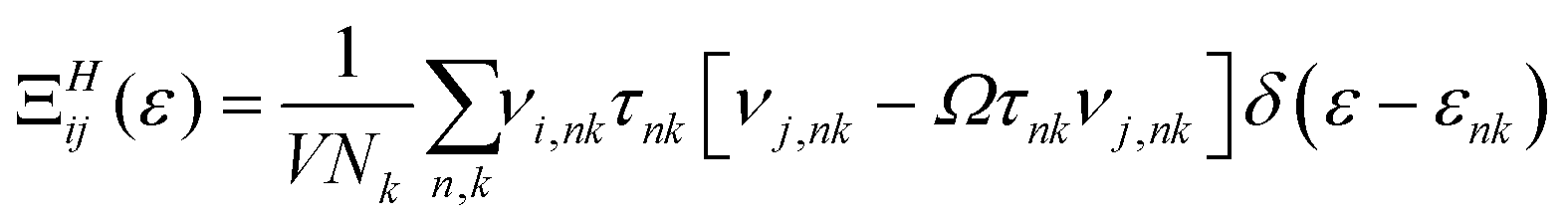 | (1) |
 that operates on velocity and relaxation time. Within BTE, response functions are defined as follows, where f is the Fermi–Dirac distribution and μ the chemical potential:
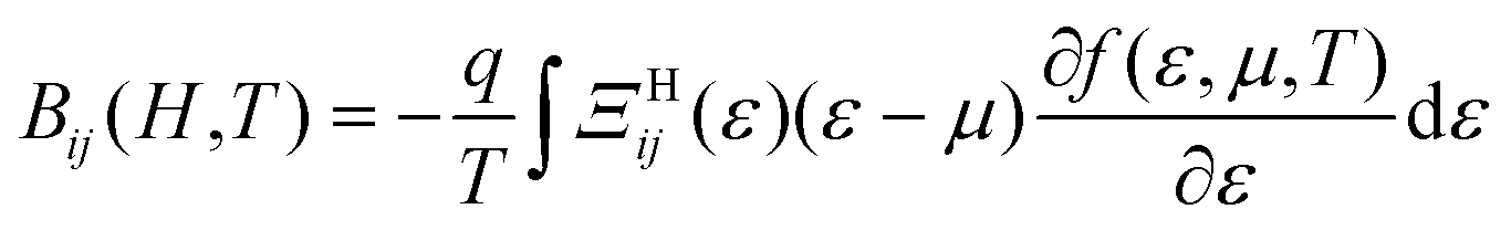 | (2) |
 | (3) |
| [Q(H,T)] = [σ(H,T)]−1[B(H,T)] | (4) |
For a detailed clarification, ref. 51 and 52 should be consulted. Eqn (1) demonstrates that the Nernst coefficient directly depends on the relaxation time which is inversely proportional to the effective mass.53,54 Moreover, analytical models prove that the magnitude of the Nernst coefficient largely grows with carrier mobility.55
First-principles calculations of layered materials were carried out using density functional theory (DFT) with a projector augmented wave method56via the Quantum Espresso package (version 7.1).57 Experimental lattice parameters were taken from the literature and the atomic positions were fully relaxed to reach the minimum energy. Van der Waals correction ‘dft-d’58,59 was applied to handle the cross-plane force between layers. While the van der Waals correction is critical to obtaining the correct interlayer spacings, we demonstrate that this correction does not affect the calculated thermomagnetic properties (cf. ESI†). Moving to the second rung of Jacob's ladder, the Engel–Vosko exchange functional60 was employed for band structure calculations. This exchange–correlation functional appeared to be relatively accurate for band gaps of solids.61 Further details of DFT calculations can be found in the ESI.†
The transport distribution function 1 needs to be assessed on a sufficiently fine mesh which was provided via maximally localized Wannier function (MLWF) basis sets as implemented in the Wannier90 package.62 ElecTra code63 was used to compute carrier mobility where both electron–phonon and ionized impurity scattering mechanisms were taken into account. Inputs to ElecTra (bulk and shear moduli, dielectric constant, phonon frequency, band gap, and deformation potentials) were taken from literature, where available (see ESI† for details). The accuracy of the calculated scattering rates was analyzed by comparing theoretical mobility to the previous experiments. Finally, the Nernst coefficient was calculated using semi-classical BTE in the presence of a magnetic field within relaxation time approximation as implemented in the NERTAW code.51,52Fig. 1 illustrates the workflow used in this work.
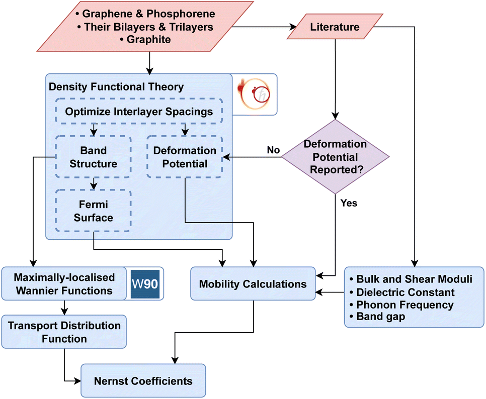 | ||
| Fig. 1 The workflow followed in this work identifies 2D materials with high Nernst coefficients. Optimal interlayer distances, band diagrams, Fermi surfaces, and deformation potential (where not available in literature) were calculated by DFT for 2D materials in the carbon and phosphor families. MLWF was utilized to calculate the transport distribution function. Bulk and shear moduli, dielectric constants, band gaps, and phonon frequencies from literature were collected to calculate the mobility. Lastly, transport distribution function and mobility were integrated to predict the Nernst coefficients in the NERTAW framework.51,52 | ||
3. Results and discussion
First, we will detail the 2D materials selection and discuss the available experimental Seebeck and Nernst effect data for the selected materials. Then we will describe the atomistic and electronic structures of the 2D materials studied and finally analyze the mobility and Nernst properties we calculated.3.1. Materials selection
Based on unique electronic properties or high room temperature Nernst coefficients in the bulk we selected promising 2D material candidates. Graphene exhibits well-known unique electronic properties such as the Dirac cone and a linear dispersion near the K point. For this reason, we consider mono-, bi-, and tri-layer graphene, as well as bulk graphite which has shown a moderately large Nernst coefficient at low temperatures (few Kelvin).64 Further, the Nernst coefficient of black phosphorus has been reported to reach an impressive value of 80 V K−1 at 280 K under a 6 Tesla magnetic field.65 We hence further consider mono-, bi-, and trilayers of black phosphorus in our analysis. Materials with a large bandgap (such as 2D MoS2 or 2D BN) were not considered since a large bandgap typically results in an insufficient presence of opposite charges within the gap and hence a negligible Nernst signal. Furthermore, we excluded 2D materials in which magnetic moments and spin–orbit coupling effects play key roles. There are a few additional 2D candidates that could be of interest for future exploration that we did not consider here due to lack of previous experimental mobility and Nernst data in both the low-dimensional and bulk polymorphs. For example, silicene, germanene, and the MoSi2N4 family66 may be of interest for future studies.Our thermomagnetic calculation workflow (cf.Fig. 1) was performed under a magnetic field of 0.4 T at room temperature (300 K) for all selected materials.
3.2. Previous literature of Seebeck and Nernst effects in selected 2D materials
Due to graphene's weak electron–phonon interaction its mobility is drastically higher than other 2D materials. Comprehensive theoretical analyses and experimental investigations suggest that the Seebeck coefficient in graphene could attain values similar to those observed in bulk semiconductors by reducing the carrier density.67 High mobility and competitive Seebeck coefficient in graphene lead to a substantial thermoelectric power factor.68 Furthermore, phenomena such as the Hall effect, quantum corrections to the conductivity, and the dynamical transport emerged to be extraordinary in graphene.69,70In contrast, there is a limited number of studies on the Nernst effect in graphene. Yan et al.71 probed the Nernst effect in graphene for Dirac fermions subjected to charged impurity scatterings and a weak magnetic field at low temperatures. The transverse thermoelectric power was found to be intricately linked with the Hall conductivity and the longitudinal thermoelectric power. Liu et al.72 introduced a systematic method for adjusting the mobility of identical graphene devices and explored how the thermomagnetic transport properties of graphene depend on carrier mobility. Distinctly enhanced Nernst signals were observed with higher mobility. From an experimental point of view, the majority of the Nernst effect in graphene has been conducted at low temperatures. The Nernst coefficient of graphene at 20 K under a magnetic field of 5 Tesla was measured to be nearly 20 μV K−1.73 In a similar study, the Nernst coefficient of graphene was reported as high as 30 μV K−1 at 200 K. To our knowledge literature lacks a thorough assessment of the thermomagnetic effects in graphene near and above room temperature.
Ma et al.74,75 numerically studied the thermoelectric and thermal transport properties in trilayer graphene with various stacking orders in the presence of a magnetic field and disorder. Specifically, in the case of biased ABA stacking, unique characteristics were observed as a result of the Landau level (LL) crossing between electron and hole bands, which strongly indicated a semimetallic band overlap. Furthermore, thermoelectric conductivities showed clear asymptotic behavior, depending on the ratio of the width of the disorder-broadened LLs to temperature. The calculated Nernst signal exhibited a prominent peak at the central LL with magnitudes on the order of kB/e. Interestingly, the sign of the Nernst signal changed at the other LLs.
Hu et al.65 presented a thorough analysis of the thermoelectric as well as thermomagnetic effects of bulk single-crystalline black phosphorus across a wide range of temperatures and magnetic fields. Below a critical temperature of approximately 250 K, electrical transport was primarily governed by extrinsic charge carriers of the hole type, exhibiting high mobility that surpasses 104 cm2 (V s)−1 at low temperatures. Thermal transport measurements exhibited a peak in-plane thermal conductivity of around 180 W (m K)−1 at roughly 25 K. As noted above, the Nernst coefficient was observed to reach a high value of 80 μV K−1 at 280 K and a 6 Tesla magnetic field. In addition to the experiments, thermomagnetic effects in bulk black phosphorus were numerically analyzed under the impact of both a magnetic field and disorder. The quantized Hall conductivity displayed similarities to that of a traditional 2D electron gas and the Nernst signals were enhanced by applying a voltage between top and bottom layers.76 Phosphorene has surfaced as a promising contender for electronic and optoelectronic devices due to its distinct in-plane anisotropy, high carrier mobility, and a customizable direct band gap.77
3.3. Atomistic and electronic structures
In this section, we will discuss the atomistic and electronic structures of the selected materials. The unit cells are displayed in Fig. 2, and the electronic structures of the carbon-family materials are plotted close to the Fermi level in Fig. 3. The full band diagrams of the carbon-family materials and the electronic structure of trilayer phosphorene are shown in ESI.†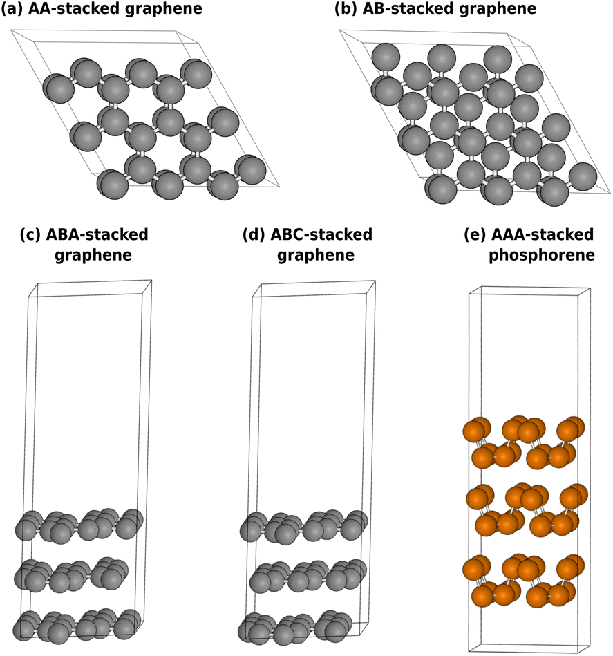 | ||
| Fig. 2 Top view of AA (a) and AB (b) stacked bilayer graphene. Side view of ABA (c) and ABC (d) stacked trilayer graphene. Armchair configuration in AAA stacked trilayer phosphorene (e). For illustration purposes, 3 × 3 × 1 and 2 × 2 × 1 supercells are shown for graphene and phosphorene, respectively. | ||
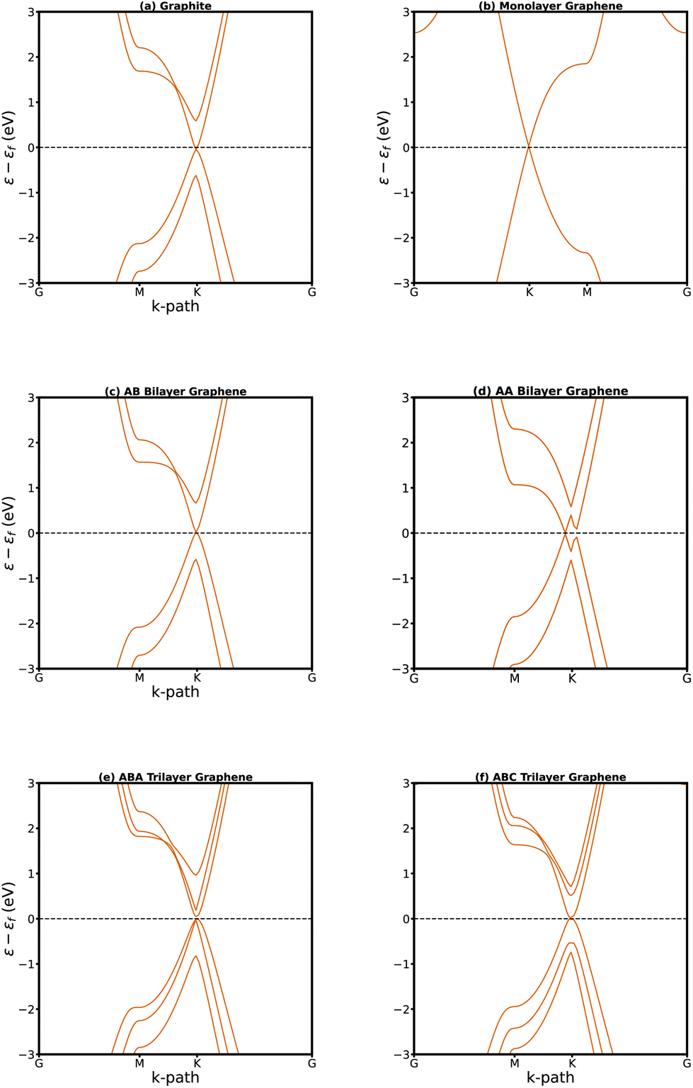 | ||
| Fig. 3 Electronic structure of graphite (a), monolayer (b), AB stacked bilayer (c), AA stacked bilayer (d), ABA stacked trilayer (e), and ABC stacked trilayer graphene (f). In each case zero is the intrinsic Fermi level. | ||
A single-layer sheet of carbon, one atom thick, forms a hexagonal lattice that gives rise to a distinctive band structure. The electronic dispersion of freestanding graphene possesses a unique conical shape near the Fermi energy, wherein the tips of these cones precisely meet at the Fermi level (Fig. 3b). This distinctive feature enables us to describe their behavior through a model of massless fermions that adhere to the principles outlined in the Dirac equation.7,78,79 The Dirac cone gives rise to remarkable charge carrier mobility in graphene.
The AB stacking of bilayer graphene is more stable than the AA stacking by a small energy difference. Unlike AA stacked (Fig. 2a), the AB stacked bilayer is an asymmetric configuration (Fig. 2b) known as Bernal. For the AB stacking, it has been observed that the interlayer coupling disrupts the symmetry and isotropy of its energy bands. This transformation results in the linear bands of monolayer graphene becoming parabolic (Fig. 3c), leading to a notable reduction in the overlap between its valence and conduction bands.80 In an AA bilayer structure, carbon atoms are situated directly above each other in successive layers. AA stacking has been experimentally observed in disordered or pregraphitic carbon, also known as turbostratic graphite.81 The AA configuration exhibits unique electronic properties, characterized by two degenerate electronic and hole bands crossing at the Fermi energy (Fig. 3d).
The ABA stacking of trilayer graphene is more stable than the ABC stacking82 (illustrated in Fig. 2c and d, respectively). It has hence been challenging to synthesize the pure ABC-stacked trilayer phase,82 despite the intriguing properties expected from this configuration. Electronic structure calculations indicate that the electronic states of trilayer graphene exhibit a significant dependence on the stacking sequence. Trilayer graphene with ABA stacking demonstrates three bands in proximity to the Fermi level (εf), with two crossing it at the K point (Fig. 3e) whereas in ABC stacking a parabolic band only touches εf at the K point (Fig. 3f).
Monolayer and bilayer phosphorene have wide band gaps (1.75 and 1.40 eV,83 respectively). However, trilayer phosphorene in the armchair configuration (illustrated in Fig. 2e) possesses a relatively narrower band gap of 1.02 eV.
3.4. Mobility and Nernst coefficient
We calculated the mobility and Nernst coefficients for mono-, bi-, and tri-layers of graphene and phosphorene and also for bulk graphite. The Nernst coefficient of bulk black phosphorus was taken from literature.65 The calculated carrier mobilities are plotted in Fig. 4 against experimental values for graphene, AB stacked bilayer graphene, graphite, and p-type single-layer phosphorene. Our theoretical results for electron mobility of monolayer graphene are in close agreement with the measurements84 at room temperature. As the electron concentration increases, there is a corresponding increase in the probability of scattering, which subsequently leads to a decrease in mobility (Fig. 4b). Similarly, the calculated mobilities of AB stacked bilayer graphene, graphite, and p-type single-layer phosphorene agree reasonably well with experimental data confirming the validity of our theoretical scattering rates.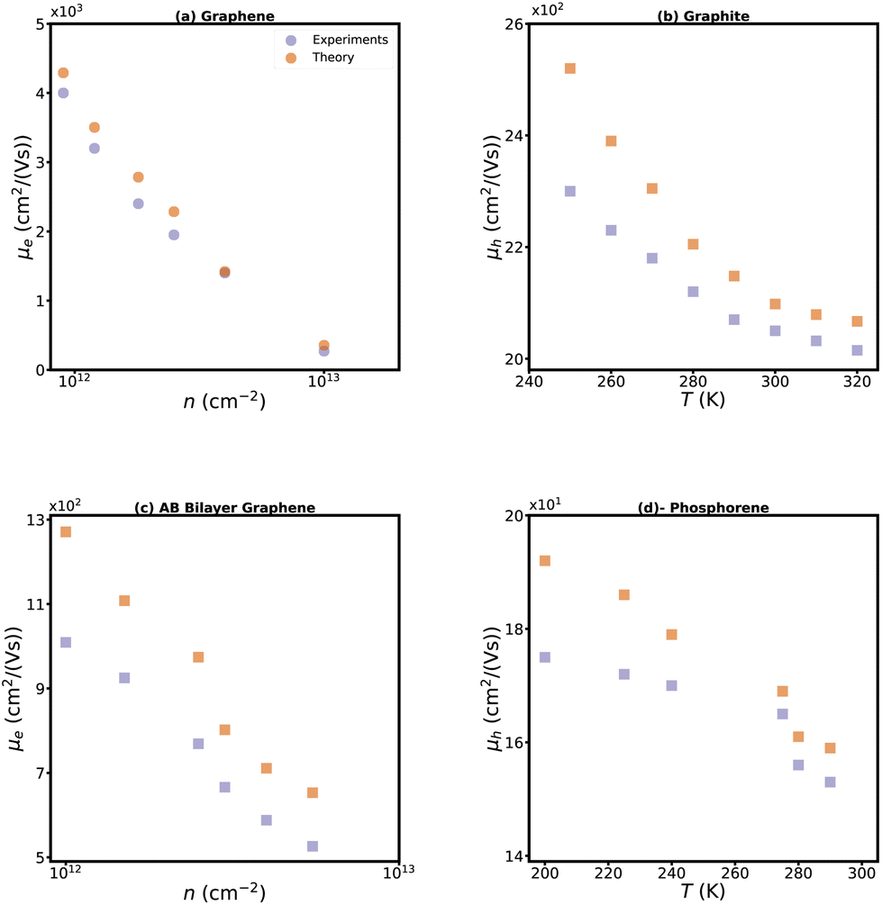 | ||
| Fig. 4 Experimental carrier mobility of monolayer graphene84 (blue circles) at T = 300 K and our theoretical results (red circles) versus carrier concentration (a). Graphite hole mobility versus temperature85 (b). Electron mobility of AB stacked bilayer graphene at room temperature versus carrier concentration86 (c). Mobility of p-type single layer phosphorene versus temperature (d).87 | ||
The maximum Nernst coefficients for each material are summarized in Fig. 5. Among various carbon stacking configurations, the p-type ABA stacked trilayer exhibits the highest Nernst coefficient of 112 μV (KT)−1 significantly larger than ABC stacked graphene (35 μV (KT)−1) and monolayer graphene (40 μV (KT)−1).
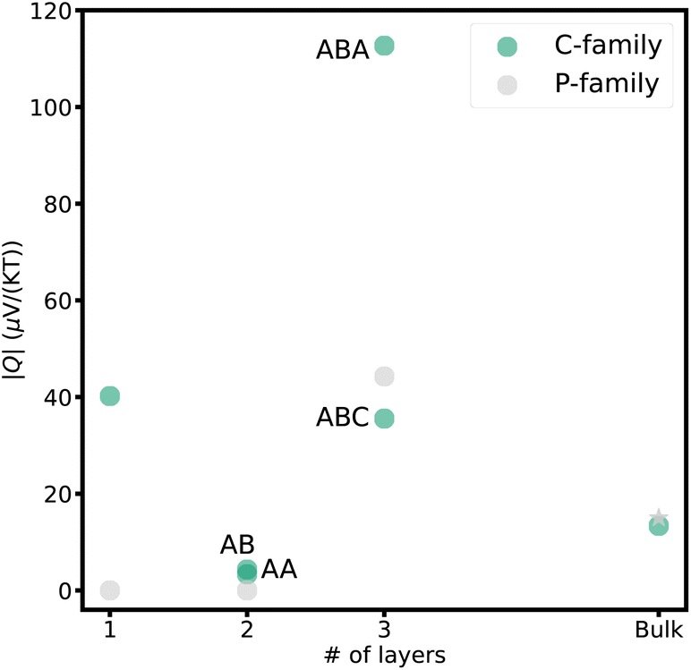 | ||
| Fig. 5 Maximum computed Nernst coefficient (absolute value) versus number of layers for carbon and phosphorous from single layers of graphene and phosphorene to graphite and bulk black phosphorous at T = 300 K. Nernst coefficient of bulk black phosphorus was taken from literature.65 | ||
Both bilayer stackings of graphene exhibit a significantly lower Nernst coefficient (∼4 μV (KT)−1) compared to monolayer graphene. For AB stacking, this is likely due to the notable reduction in the overlap between its valence and conduction bands (discussed in the previous section and shown in Fig. 3c) decreasing the charge carrier mobility. The electronic structure of AA stacked bilayer graphene gives rise to various electron and electron–phonon instabilities, including a shear-shift instability.88 Such instabilities along with the degenerate bands lead to smaller Nernst coefficients.
The exceptionally large Nernst coefficient of ABA-stacked graphene is likely attributed to high hole mobility due to the presence of a Dirac cone89 (linear energy dispersion around εf) at the inner bands and additional bands at the intrinsic Fermi level, resulting in the coexistence of holes and electrons. Substantial carrier mobilities coupled with significant quantities of opposite charges that will be generated lead to an exceptionally large Nernst coefficient. Conversely, in trilayer graphene with ABC stacking, a parabolic band touches εf at the K point (Fig. 3f) which particularly lowers carrier mobility. As a result, the Nernst coefficient becomes smaller than that of the ABA stacked counterpart.
The phosphorene family consists of semiconductors with band gaps that vary significantly depending on the number of layers. Monolayer and bilayer phosphorene have wide band gaps, resulting in insufficient carrier concentrations and hence a Nernst voltage of zero. However, trilayer phosphorene has a narrower band gap of 1.02 eV,83 allowing opposite carriers to coexist in the gap. Additionally, the higher hole mobility87 results in a substantial Nernst voltage in p-doped trilayer phosphorene of 44 μV (KT)−1, which is larger than the experimentally observed Nernst voltage for the bulk, 15 μV (KT)−1.
The detailed dependencies of the Nernst coefficients Q with carrier concentration are plotted in Fig. 6 and 7 for carbon-family materials and trilayer phosphorene, respectively. The maximum Nernst coefficient of Fig. 6 and 7 are summarized in Fig. 5 for each material.
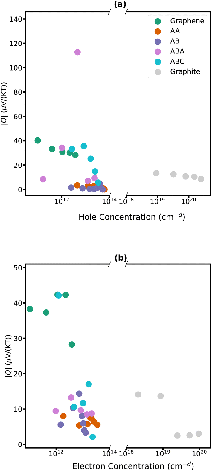 | ||
| Fig. 6 Nernst coefficient of monolayer (green), AA stacked bilayer (orange), AB stacked bilayer (blue), ABA stacked trilayer (pink), ABC stacked trilayer (cyan) graphene, and graphite (silver) for a range of hole concentrations (a) and electron concentrations (b) at T = 300 K. Concentrations are in units of cm−d where d is 3 for graphite and 2 for all other materials. | ||
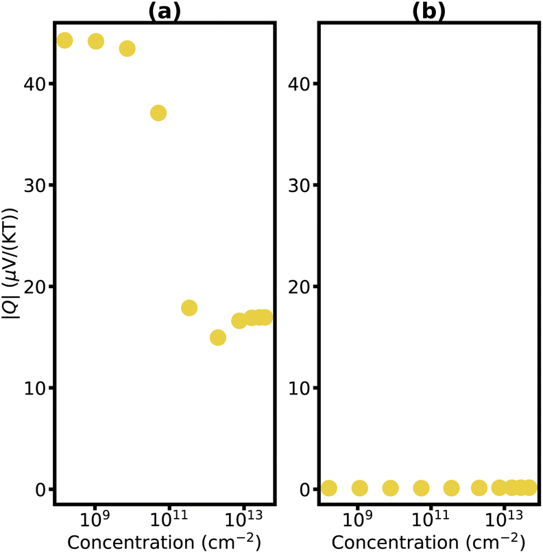 | ||
| Fig. 7 Nernst coefficient of AAA stacked trilayer phosphorene versus charge carrier concentration for p-type (a) and n-type (b) at T = 300 K. | ||
Eqn (1) demonstrates that the Nernst coefficient depends on not only the band features and the number of states but also the relaxation time. A large Nernst coefficient in semiconductors is typically associated with the coexistence of both charge carriers, electrons and holes. As the chemical potential delves too deep into the bands, one type of charge carriers becomes dominant – holes in the valence bands and electrons in the conduction band. This transition results in a decrease in the magnitude of the Nernst coefficient at high carrier concentrations, and larger Nernst signals at semiconductors are frequently observed near the intrinsic Fermi level.90 It is interesting to note, that for trilayer phosphorene as the holes become the dominant carriers and their concentration rises, there is a subsequent decrease in mobility, causing a diminution of the Nernst coefficient (Fig. 7b).
4. Conclusions
In this work, we have selected promising 2D materials and revealed that few-layer graphene and phosphorene exhibit large Nernst coefficients at room temperature. Specifically, the largest Nernst coefficient was predicted for trilayer graphene with the ABA stacking (112 μV (KT)−1), followed by trilayer phosphorene (44 μV (KT)−1) and then monolayer graphene (40 μV (KT)−1) and trilayer graphene with the ABC stacking (35 μV (KT)−1). Our first-principles calculations have shown that the layer stacking order in trilayer graphene significantly affects the magnitude of the Nernst effect due to the distinct band structure features close to the Fermi level. Moreover, our predicted mobilities agree well with experimentally observed mobilities in the 2D materials, validating our ab initio calculation framework. This work paves the way toward large Nernst effect materials in next-generation cryogenic cooling devices and facilitates materials selection for thermomagnetic and thermoelectric applications.Author contributions
S. Emad Rezaei: Investigation (lead); methodology (lead); visualization (equal); writing – original draft preparation (lead); writing – review and editing (equal); conceptualization (equal). Peter Schindler: Supervision (lead); conceptualization (equal); visualization (equal); writing – review and editing (equal); resources (lead).Conflicts of interest
There are no conflicts to declare.Acknowledgements
The authors acknowledge the start-up funding from the Department of Mechanical and Industrial Engineering at Northeastern University. This work was completed in part using the Discovery cluster, supported by Northeastern University's Research Computing team.References
- G. Iannaccone, F. Bonaccorso, L. Colombo and G. Fiori, Nat. Nanotechnol., 2018, 13, 183–191 CrossRef CAS PubMed.
- K. F. Mak and J. Shan, Nat. Photonics, 2016, 10, 216–226 CrossRef CAS.
- P. Chen, T. L. Atallah, Z. Lin, P. Wang, S.-J. Lee, J. Xu, Z. Huang, X. Duan, Y. Ping and Y. Huang, et al., Nature, 2021, 599, 404–410 CrossRef CAS PubMed.
- A. Gupta, T. Sakthivel and S. Seal, Prog. Mater. Sci., 2015, 73, 44–126 CrossRef CAS.
- A. Pospischil, M. M. Furchi and T. Mueller, Nat. Nanotechnol., 2014, 9, 257–261 CrossRef CAS PubMed.
- V. K. Sangwan and M. C. Hersam, Annu. Rev. Phys. Chem., 2018, 69, 299–325 CrossRef CAS PubMed.
- S. Lee, D. Broido, K. Esfarjani and G. Chen, Nat. Commun., 2015, 6, 6290 CrossRef CAS PubMed.
- X. Wang, M. Zebarjadi and K. Esfarjani, Sci. Rep., 2018, 8, 9303 CrossRef PubMed.
- E. R. Antoniuk, Y. Yue, Y. Zhou, P. Schindler, W. A. Schroeder, B. Dunham, P. Pianetta, T. Vecchione and E. J. Reed, Phys. Rev. B, 2020, 101, 235447 CrossRef CAS.
- G. S. Na and H. Chang, npj Comput. Mater., 2022, 8, 1–11 CrossRef.
- P. Schindler, D. C. Riley, I. Bargatin, K. Sahasrabuddhe, J. W. Schwede, S. Sun, P. Pianetta, Z.-X. Shen, R. T. Howe and N. A. Melosh, ACS Energy Lett., 2019, 4, 2436–2443 CrossRef CAS PubMed.
- P. Schindler, E. R. Antoniuk, G. Cheon, Y. Zhu and E. J. Reed, Discovery of materials with extreme work functions by high-throughput density functional theory and machine learning, 2020, arXiv:2011.10905.
- Y. Ouyang, Z. Zhang, D. Li, J. Chen and G. Zhang, Ann. Phys., 2019, 531, 1800437 CrossRef CAS.
- L. Yang, Z.-G. Chen, M. S. Dargusch and J. Zou, Adv. Energy Mater., 2018, 8, 1701797 CrossRef.
- B. Hinterleitner, I. Knapp, M. Poneder, Y. Shi, H. Müller, G. Eguchi, C. Eisenmenger-Sittner, M. Stöger-Pollach, Y. Kakefuda and N. Kawamoto, et al., Nature, 2019, 576, 85–90 CrossRef CAS PubMed.
- Q. Wang, R. Quhe, Z. Guan, L. Wu, J. Bi, P. Guan, M. Lei and P. Lu, RSC Adv., 2018, 8, 21280–21287 RSC.
- A. Patel, D. Singh, Y. Sonvane, P. Thakor and R. Ahuja, ACS Appl. Mater. Interfaces, 2020, 12, 46212–46219 CrossRef CAS PubMed.
- H. Ohta, S. W. Kim, S. Kaneki, A. Yamamoto and T. Hashizume, Adv. Sci., 2018, 5, 1700696 CrossRef PubMed.
- M. Markov and M. Zebarjadi, Nanoscale Microscale Thermophys. Eng., 2019, 23, 117–127 CrossRef CAS.
- Y. Pang, E. Rezaei, D. Chen, S. Li, Y. Jian, Q. Wang, Z. Wang, J. Duan, M. Zebarjadi and Y. Yao, Phys. Rev. Mater., 2020, 4, 094205 CrossRef CAS.
- D.-Y. Chung, T. Hogan, P. Brazis, M. Rocci-Lane, C. Kannewurf, M. Bastea, C. Uher and M. G. Kanatzidis, Science, 2000, 287, 1024–1027 CrossRef CAS PubMed.
- R. Venkatasubramanian, E. Siivola, T. Colpitts and B. O′quinn, Nature, 2001, 413, 597–602 CrossRef CAS PubMed.
- J. Duan, X. Wang, X. Lai, G. Li, K. Watanabe, T. Taniguchi, M. Zebarjadi and E. Y. Andrei, Proc. Natl. Acad. Sci. U. S. A., 2016, 113, 14272–14276 CrossRef CAS PubMed.
- Q.-Y. Li, Q. Hao, T. Zhu and M. Zebarjadi, Eng. Sci., 2020, 13, 24–50 Search PubMed.
- A. Ettingshausen and W. Nernst, Ann. Phys. Chem., 1886, 265, 343 CrossRef.
- A. W. Smith, Phys. Rev., 1911, 33(Series I), 295 Search PubMed.
- A. W. Smith, Phys. Rev., 1916, 8, 79 CrossRef CAS.
- A. W. Smith, Phys. Rev., 1921, 17, 23 CrossRef CAS.
- H. Mette, W. W. Gärtner and C. Loscoe, Phys. Rev., 1960, 117, 1491 CrossRef CAS.
- H. Mette, W. W. Gärtner and C. Loscoe, Phys. Rev., 1959, 115, 537 CrossRef CAS.
- H. N. H. Nakamura, K. I. K. Ikeda and S. Y. S. Yamaguchi, Jpn. J. Appl. Phys., 1999, 38, 5745 CrossRef CAS.
- M. Yazdani-Asrami, A. Sadeghi and M. D. Atrey, Int. J. Refrig., 2022, 140, 70–81 CrossRef.
- F. Jazaeri, A. Beckers, A. Tajalli and J.-M. Sallese, 2019 MIXDES-26th International Conference “Mixed Design of Integrated Circuits and Systems”, 2019, pp. 15–25.
- M. M. H. Polash and D. Vashaee, Phys. Rev. Appl., 2021, 15, 014011 CrossRef CAS.
- Y. Sakuraba, K. Hasegawa, M. Mizuguchi, T. Kubota, S. Mizukami, T. Miyazaki and K. Takanashi, Appl. Phys. Express, 2013, 6, 033003 CrossRef.
- Y. Sakuraba, Scr. Mater., 2016, 111, 29–32 CrossRef CAS.
- M. Mizuguchi and S. Nakatsuji, Sci. Technol. Adv. Mater., 2019, 20, 262–275 CrossRef CAS PubMed.
- H. Goldsmid and K. Sydney, J. Phys. D: Appl. Phys., 1971, 4, 869 CrossRef CAS.
- J. Xu, W. A. Phelan and C.-L. Chien, Nano Lett., 2019, 19, 8250–8254 CrossRef CAS PubMed.
- G. Sharma, Phys. Rev. B, 2018, 98, 075416 CrossRef CAS.
- S. N. Guin, K. Manna, J. Noky, S. J. Watzman, C. Fu, N. Kumar, W. Schnelle, C. Shekhar, Y. Sun and J. Gooth, et al., NPG Asia Mater., 2019, 11, 16 CrossRef CAS.
- R. Syariati, S. Minami, H. Sawahata and F. Ishii, APL Mater., 2020, 8, 041105 CrossRef CAS.
- T. Song, Y. Jia, G. Yu, Y. Tang, P. Wang, R. Singha, X. Gui, A. J. Uzan, M. Onyszczak, K. Watanabe, et al., arXiv preprint arXiv:2303.06540, 2023.
- S. M. Wu, A. Luican-Mayer and A. Bhattacharya, Appl. Phys. Lett., 2017, 111, 223109 CrossRef.
- M. Li, Z. Wang, D. Zhao, Y. Liu, C. Jiang, T. Wu, Q. Tao, G.-H. Cao and Z.-A. Xu, Phys. Rev. B, 2022, 105, 104512 CrossRef CAS.
- T. Zhu, P. M. Litwin, M. G. Rosul, D. Jessup, M. S. Akhanda, F. F. Tonni, S. Krylyuk, A. V. Davydov, P. Reinke and S. J. McDonnell, et al., Mater. Today Phys., 2022, 27, 100789 CrossRef CAS.
- P. Dollfus, V. H. Nguyen and J. Saint-Martin, J. Phys.: Condens. Matter, 2015, 27, 133204 CrossRef PubMed.
- Y. Xing, Q.-F. Sun and J. Wang, Phys. Rev. B: Condens. Matter Mater. Phys., 2009, 80, 235411 CrossRef.
- J. G. Checkelsky and N. Ong, Phys. Rev. B: Condens. Matter Mater. Phys., 2009, 80, 081413 CrossRef.
- M. S. Akhanda, S. Krylyuk, D. A. Dickie, A. V. Davydov, F. Han, M. Li and M. Zebarjadi, Mater. Today Phys., 2022, 29, 100918 CrossRef CAS.
- S. E. Rezaei, M. Zebarjadi and K. Esfarjani, Comput. Mater. Sci., 2022, 210, 111412 CrossRef CAS.
- S. E. Rezaei, M. Zebarjadi and K. Esfarjani, Comput. Mater. Sci., 2023, 225, 112193 CrossRef CAS.
- Theory of electron transport in semiconductors: a pathway from elementary physics to nonequilibrium Green functions, ed. C. Jacoboni, Springer Science & Business Media, New York, 2010 Search PubMed.
- M. Lundstrom, Fundamentals of carrier transport, Cambridge university press, 2009 Search PubMed.
- M. Zebarjadi, S. E. Rezaei, M. S. Akhanda and K. Esfarjani, Phys. Rev. B, 2021, 103, 144404 CrossRef CAS.
- P. E. Blöchl, Phys. Rev. B: Condens. Matter Mater. Phys., 1994, 50, 17953 CrossRef PubMed.
- P. Giannozzi, S. Baroni, N. Bonini, M. Calandra, R. Car, C. Cavazzoni, D. Ceresoli, G. L. Chiarotti, M. Cococcioni and I. Dabo, et al., J. Phys.: Condens. Matter, 2009, 21, 395502 CrossRef PubMed.
- V. Barone, M. Casarin, D. Forrer, M. Pavone, M. Sambi and A. Vittadini, J. Comput. Chem., 2009, 30, 934–939 CrossRef CAS PubMed.
- S. Grimme, J. Comput. Chem., 2006, 27, 1787–1799 CrossRef CAS PubMed.
- E. Engel and S. H. Vosko, Phys. Rev. B: Condens. Matter Mater. Phys., 1993, 47, 13164 CrossRef CAS PubMed.
- P. Borlido, J. Schmidt, A. W. Huran, F. Tran, M. A. Marques and S. Botti, npj Comput. Mater., 2020, 6, 96 CrossRef CAS.
- A. A. Mostofi, J. R. Yates, Y.-S. Lee, I. Souza, D. Vanderbilt and N. Marzari, Comput. Phys. Commun., 2008, 178, 685–699 CrossRef CAS.
- P. Graziosi, Z. Li and N. Neophytou, Comput. Phys. Commun., 2023, 287, 108670 CrossRef CAS.
- Z. Zhu, H. Yang, B. Fauque, Y. Kopelevich and K. Behnia, Nat. Phys., 2010, 6, 26–29 Search PubMed.
- S. Hu, J. Xiang, M. Lv, J. Zhang, H. Zhao, C. Li, G. Chen, W. Wang and P. Sun, Phys. Rev. B, 2018, 97, 045209 CrossRef CAS.
- B. Mortazavi, B. Javvaji, F. Shojaei, T. Rabczuk, A. V. Shapeev and X. Zhuang, Nano Energy, 2021, 82, 105716 CrossRef CAS.
- J. Duan, X. Wang, X. Lai, G. Li, K. Watanabe, T. Taniguchi, M. Zebarjadi and E. Y. Andrei, Proc. Natl. Acad. Sci. U. S. A., 2016, 113, 14272–14276 CrossRef CAS PubMed.
- M. Markov and M. Zebarjadi, Nanoscale Microscale Thermophys. Eng., 2019, 23, 117–127 CrossRef CAS.
- T. Ando, Phys. E, 2007, 40, 213–227 CrossRef CAS.
- B. K. Sharma, Emerging Mater. Res., 2020, 9, 564–617 CrossRef.
- X.-Z. Yan and C. Ting, Phys. Rev. B: Condens. Matter Mater. Phys., 2010, 81, 155457 CrossRef.
- X. Liu, D. Wang, P. Wei, L. Zhu and J. Shi, Phys. Rev. B: Condens. Matter Mater. Phys., 2012, 86, 155414 CrossRef.
- J. G. Checkelsky and N. Ong, Phys. Rev. B: Condens. Matter Mater. Phys., 2009, 80, 081413 CrossRef.
- R. Ma, L. Sheng, M. Liu and D. Sheng, Phys. Rev. B: Condens. Matter Mater. Phys., 2012, 86, 115414 CrossRef.
- R. Ma and L. Wang, Eur. Phys. J. B, 2012, 85, 1–5 CrossRef.
- R. Ma, S. Liu, M. Deng, L. Sheng, D. Xing and D. Sheng, Phys. Rev. B, 2018, 97, 075407 CrossRef.
- C. Chowdhury and A. Datta, J. Phys. Chem. Lett., 2017, 8, 2909–2916 CrossRef CAS PubMed.
- B. Liao, M. Zebarjadi, K. Esfarjani and G. Chen, Phys. Rev. B: Condens. Matter Mater. Phys., 2013, 88, 155432 CrossRef.
- I. Pletikosić, M. Kralj, P. Pervan, R. Brako, J. Coraux, A. N′diaye, C. Busse and T. Michely, Phys. Rev. Lett., 2009, 102, 056808 CrossRef PubMed.
- Y. Xu, X. Li and J. Dong, Nanotechnology, 2010, 21, 065711 CrossRef PubMed.
- E. Silva, M. Santos, J. Skelton, T. Yang, T. Santos, S. Parker and A. Walsh, Mater. Today: Proc., 2020, 20, 373–382 CAS.
- K. Sugawara, N. Yamamura, K. Matsuda, W. Norimatsu, M. Kusunoki, T. Sato and T. Takahashi, NPG Asia Mater., 2018, 10, e466–e466 CrossRef CAS.
- J. Island and A. Castellanos-Gomez, 2D Materials, Elsevier, 2016, vol. 95, pp. 279–303 Search PubMed.
- J. H. Gosling, O. Makarovsky, F. Wang, N. D. Cottam, M. T. Greenaway, A. Patanè, R. D. Wildman, C. J. Tuck, L. Turyanska and T. M. Fromhold, Commun. Phys., 2021, 4, 30 CrossRef CAS.
- C. A. Klein and W. D. Straub, Phys. Rev., 1961, 123, 1581 CrossRef CAS.
- S. Xiao, J.-H. Chen, S. Adam, E. D. Williams and M. S. Fuhrer, Phys. Rev. B: Condens. Matter Mater. Phys., 2010, 82, 041406 CrossRef.
- H. Liu, A. T. Neal, Z. Zhu, Z. Luo, X. Xu, D. Tománek and P. D. Ye, ACS Nano, 2014, 8, 4033–4041 CrossRef CAS PubMed.
- A. Rakhmanov, A. Rozhkov, A. Sboychakov and F. Nori, Phys. Rev. Lett., 2012, 109, 206801 CrossRef CAS PubMed.
- W. Zhu, V. Perebeinos, M. Freitag and P. Avouris, Phys. Rev. B: Condens. Matter Mater. Phys., 2009, 80, 235402 CrossRef.
- M. S. Akhanda, S. E. Rezaei, K. Esfarjani, S. Krylyuk, A. V. Davydov and M. Zebarjadi, Phys. Rev. Mater., 2021, 5, 015403 CrossRef CAS PubMed.
Footnote |
| † Electronic supplementary information (ESI) available. See DOI: https://doi.org/10.1039/d3nr06127b |
| This journal is © The Royal Society of Chemistry 2024 |