DOI:
10.1039/D3NR05904A
(Paper)
Nanoscale, 2024,
16, 7225-7236
GeSn-on-GaAs with photoconductive carrier lifetime >400 ns: role of substrate orientation and atomistic simulation
Received
20th November 2023
, Accepted 15th March 2024
First published on 15th March 2024
Abstract
Group IV GeSn quantum material finds application in electronics and silicon-compatible photonics. Synthesizing these materials with low defect density and high carrier lifetime is a potential challenge due to lattice mismatch induced defects and tin segregation at higher growth temperature. Recent advancements in the growth of these GeSn materials on Si, Ge, GaAs, and with substrate orientations, demonstrated different properties using epitaxial and chemical deposition methods. This article addresses the effect of GaAs substrate orientation and misorientation on the materials’ properties and carrier lifetimes in epitaxial Ge0.94Sn0.06 layers. With starting GaAs substrates of (100)/2°, (100)/6°, (110) and (111)A orientations, Ge0.94Sn0.06 epitaxial layers were grown with an intermediate Ge buffer layer by molecular beam epitaxy and analyzed by several analytical tools. X-ray analysis displayed good crystalline quality, and Raman spectroscopy measurements showed blue shifts in phonon wavenumber due to biaxial compressive strain in Ge0.94Sn0.06 epilayers. Cross-sectional transmission electron microscopy analysis confirmed the defect-free heterointerface of Ge0.94Sn0.06/Ge/GaAs heterostructure. Minority carrier lifetimes of the unintentionally doped n-type Ge0.94Sn0.06 epilayers displayed photoconductive carrier lifetimes of >400 ns on (100)/6°, 319 ns on (100)/2°, and 434 ns on (110) GaAs substrate at 1500 nm excitation wavelength. On the other hand, Ge0.94Sn0.06 layer showed poor carrier lifetime on (111)A GaAs substrate. The observed differences in carrier lifetimes were correlated with the formation energy of the Ge on (100)/6° and (100)/2° GaAs heterointerface using Stillinger–Weber interatomic potential model-based atomistic simulation with different heterointerfacial bonding by Synopsys QuantumATK tool. Total energy computation of 6280-atom Ge/GaAs supercell on (100)/6° leads to lower formation energy than (100)/2°, making it more thermodynamically stable. Hence, the growth of the GeSn/III–V material system using misoriented (100) substrates that are more thermodynamically stable will enhance the performances of optoelectronic devices.
1. Introduction
Group IV based semiconductors are widely used for silicon-compatible photonics and recently pushed for long wavelength photodetector applications.1–14 Among these semiconductors, germanium-tin (GeSn) material with tunable Sn composition is at the forefront to achieve high-performance detectors and lasers. Several growth methods were developed to produce high Sn compositional Ge1−ySny materials.4–8,10,12,14,15 However, device quality Ge1−ySny materials on silicon (Si) with low defect density and high carrier lifetime are in their infancy. Researchers are looking for an alternative approach to produce GeSn materials with high carrier lifetimes: either lattice matched to underlying substrate or buffer layer16–18 or compressively strained GeSn layers.7,8,14 Among these approaches, substrate orientation and misorientation mediated GeSn materials with high carrier lifetime and low defect density have never been demonstrated. There are variations in the semiconductor properties like carrier lifetime (τ), mobility (μ), conductivity, surface state density (Nss), and density of interface states (Dit), based on crystal orientation.19–23 For instance, it is noted that among (100), (110), and (111) crystal orientations, the (110) surface is least conductive in Si, Ge, and GaAs wafers, and Nss is least for (100) surfaces in Ge and Si.19,21 In addition, the epitaxial Ge layers when grown on oriented and misoriented GaAs substrates exhibit different materials properties24–26 and metal–oxide-semiconductor capacitor properties.27,28 For instance, carrier lifetime can affect optoelectronic device performances such as internal quantum efficiency, responsivity, and heterojunction leakage in a photodetector,1,2,17 and internal/external quantum efficiency, optical gain, and material loss in a laser.1,2 In addition, high carrier lifetime signifies low leakage current due to Dit and Nss in a transistor.20,23,27 Moreover, the current Si non-planar devices like fin field effect transistors (FinFETs), gate-all-around FETs, and nanosheet FETs utilize (100) and (110) orientations.29–36 Furthermore, substrate misorientations (100)/2° towards 〈110〉 direction have an impact on these properties,37–39 which becomes crucial in heterostructure material systems.
In this work, the substrate orientation mediated epitaxial GeSn layers were grown on GaAs substrates with (100)/2°, (100)/6°, (110) and (111)A orientations using interconnected solid source molecular beam epitaxy (MBE). An intermediate Ge buffer layer was grown in between GeSn and GaAs substrate. The main objective is to improve the carrier lifetime in GeSn materials and its relationship with orientation and misorientation of the starting GaAs substrates. Epitaxial GeSn materials were characterized by several analytical tools such as X-ray analysis for composition and materials quality, cross-sectional transmission electron microscopy (TEM) for defect microstructure and heterointerface of GeSn/Ge/GaAs, Raman spectroscopy for GeSn vibrational properties, and microwave-reflection photoconductive decay (μ-PCD) technique for carrier lifetime. In addition to these measurements, carrier lifetimes were extracted as a function of orientation and misorientation with two different excitation wavelengths: 1500 nm and 1800 nm. To relate these excitation wavelengths, density functional theory (DFT) calculations were performed using Synopsys QuantumATK tool, determining the energy band gaps from the electronic band structure of GeSn-based heterostructures studied here. Minority carrier lifetimes of the unintentionally doped n-type Ge0.94Sn0.06 epilayers displayed carrier lifetimes of >400 ns on (100)/6°, 319 ns on (100)/2°, and 434 ns on (110) GaAs substrate at 1500 nm excitation wavelength. The observed differences in carrier lifetimes with misorientation were correlated with the formation energy of the Ge on (100)/6° and (100)/2° GaAs substrates using Stillinger–Weber interatomic potential model-based atomistic simulation with different heterointerfacial bonding by Synopsys QuantumATK tool.40,41 Total energy computation of 6280-atom Ge/GaAs supercell on (100)/6° leads to lower formation energy than (100)2°, making it more thermodynamically stable and hence higher carrier lifetime. The heterointerface atomic bonding and its formation energy will open an opportunity to implement on other semiconductors substrate orientation mediated material systems.
2. Experimental
2.1. Material synthesis
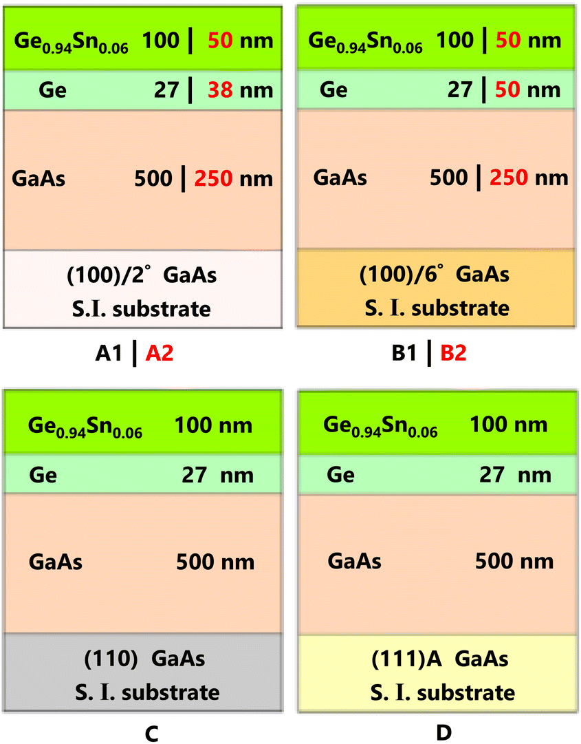
Heteroepitaxial Ge0.94Sn0.06/Ge layers were grown over (100)/2°, (100)/6°, (110), and (111)A semi-insulating GaAs substrates using a dual chamber vacuum interconnected solid source MBE system. The substrate offcut (i.e., misorientation) degrees noted here are towards the [110] direction, and (111)A denotes Ga-terminated substrate. Note that there were no misorientation angles associated with the (110) and (111)A GaAs substrates. Group IV and III–V growth chambers are interconnected but isolated via an ultra-high-vacuum transfer chamber to prevent mutual interdiffusion originating from either of the chambers as well as prevent oxidation of the III–V surface prior to either Ge or GeSn layer growth. Fig. 1 presents the schematic of each Ge0.94Sn0.06/Ge/GaAs heterostructure material system analyzed in this work, beginning with: (i) sample A1 (A2) – 100 (50) nm thick epitaxial Ge0.94Sn0.06 grown on 27 (38) nm Ge buffer on (100)/2° GaAs substrate; (ii) sample B1 (B2) – 100 (50) nm thick epitaxial Ge0.94Sn0.06 grown on 27 (50) nm Ge buffer on (100)/6° GaAs substrate; (iii) samples C and D – each has 100 nm thick epitaxial Ge0.94Sn0.06 grown on 27 nm Ge buffer on (110) and (111)A GaAs substrates, respectively. The epitaxial Ge0.94Sn0.06 layers are pseudomorphic with ∼0.81% compressive strain and an unintentional doping of n-type with donor concentration ∼1018 cm−3 determined via Hall effect measurement using the van der Pauw method.
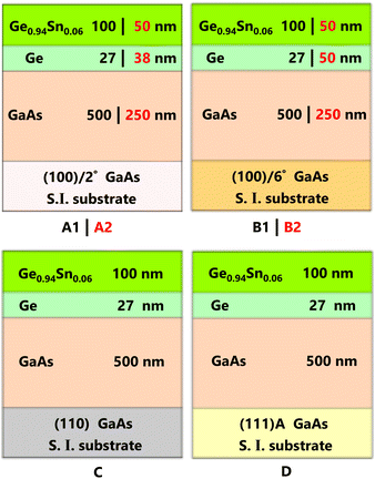 |
| | Fig. 1 Cross-sectional schematics of Ge0.94Sn0.06/Ge/GaAs heterostructures with differently orientated and misoriented semi-insulating (S.I.) GaAs substrates, analyzed in this work: A1 (A2) – 100 (50) nm thick epitaxial Ge0.94Sn0.06 layer grown on 27 (38) nm Ge buffer with (100)/2° orientation; B1 (B2) – 100 (50) nm thick epitaxial Ge0.94Sn0.06 layer grown on 27 (50) nm Ge buffer with (100)/6° orientation; C and D – 100 nm thick Ge0.94Sn0.06 grown on 27 nm Ge buffer with (110) and (111)A orientations, respectively. The Ge0.94Sn0.06 epilayers are ∼0.81% compressively strained. | |
GaAs substrates oxide desorption was performed in the temperature range of 750 °C to 765 °C with arsenic overpressure of ∼10−5 torr, and reflection high energy electron diffraction (RHEED) system was used to monitor the surface reconstruction during oxide desorption as well as GaAs layer growth. The temperature referred to here is the thermocouple temperature. Arsenic (As2) overpressure of ∼10−5 torr was maintained during the oxide desorption to compensate volatile escape of arsenic from the surface of the GaAs substrate. While samples A2-(100)/2° and B2-(100)/6° were grown separately on a 3-inch substrate, to have a leveling point of comparison: samples A1-(100)/2°, B1-(100)/6°, C-(110) and D-(111)A were mounted together on a molybdenum plate with indium. The lower oxide desorption temperature (750 °C) was set for samples grown on epi-ready 3-inch GaAs wafers (A2 and B2) than other samples (A1, B1, C, D) under As2 overpressure. During this process, surface reconstruction of (2 × 4) was monitored using RHEED, and the substrate temperature was decreased to ∼650 °C for undoped homoepitaxial GaAs layer growth. The growth rate of 0.50 μm h−1 and As2/Ga flux ratio of ∼32 was maintained during growth for all the samples studied here. Streaky (2 × 4) surface reconstruction was observed from the surface of (100)GaAs after the homoepitaxial growth of GaAs. After the growth, each sample was cooled down to 300 °C under arsenic overpressure and then further cooled down below 150 °C prior to transfer to the group IV chamber via vacuum interconnected transfer chamber under ultra-high vacuum of ∼ 4 × 10⁻¹⁰ torr for Ge and Ge0.94Sn0.06 layer growth.
The 400 g SUMO® Ge effusion cell and standard tin effusion cell were used for the Ge and GeSn layer growth. The growth rate of Ge thin film was calibrated to be ∼0.1 Å s−1. Samples A1-(100)/2°, B1-(100)/6°, C-(110) and D-(111)A were grown at the substrate temperature of 150 °C for the 27 nm Ge layer. The 100 nm Ge0.94Sn0.06 layer for samples A1, B1, C and D was grown at two-step growth temperature (50 nm at 150 °C and 50 nm at 185 °C), as shown in Table 1. Whereas for sample A2-(100)/2° it was maintained at 195 °C during the growth of 38 nm Ge and bottom 25 nm Ge0.94Sn0.06, and 190 °C for the topmost 25 nm Ge0.94Sn0.06 layer. For sample B2-(100)/6°, a constant temperature of 225 °C was maintained for both 50 nm Ge and 50 nm GeSn epilayers. After GeSn layer growth, each sample was cooled down below 50 °C at a ramp rate of ∼5 °C min−1 to avoid thermal cracking due to differences in thermal expansion coefficient mismatch of different materials used in the layer stack.
Table 1 Ge0.94Sn0.06/Ge/GaAs heterostructure material systems with different orientation
| Sample |
GaAs substrate |
Thickness (nm) Ge0.94Sn0.06/Ge /GaAs |
Ge0.94Sn0.06 growth temp. (°C) |
|
A1
|
(100)/2° |
100/27/500 |
50 nm
|
185 |
|
B1
|
(100)/6° |
|
C
|
(110) |
50 nm
|
150 |
|
D
|
(111)A |
|
A2
|
(100)/2° |
50/38/250 |
25 nm
|
190 |
|
25 nm
|
195 |
|
B2
|
(100)/6° |
50/50/250 |
225 |
2.2. Material analysis
X-ray analysis was performed on selected samples to determine the Sn and strain composition as well as the overall structural quality of the layer using PANalytical X'Pert Pro X-ray unit equipped with pixel and proportional detector. Vibrational properties of the materials were studied using Raman spectroscopy at room temperature. The measurements were carried out in the backscattering geometry utilizing the JY Horiba LabRam HR800 instrument setup. This system uses an Ar+ (514.48 nm) laser that operates with ∼65 mW output power at the source, and the laser power that irradiates the sample surface was ∼7 mW. A 100× objective lens was used to focus the laser on each sample surface, and the size of the diffraction grating to detect the scattered light was 1800 g mm−1 (grooves per millimeter). A standard silicon sample was used to calibrate the instrument prior to measuring the intended GeSn samples: the Si–Si LO (longitudinal optical) phonon peak was found at ω0,Si = 520.67 cm−1 (ref. 42) at a spectral shift resolution of 0.003 cm−1. This inelastic Stokes scattering phenomenon was recorded by collecting the data for 10 seconds each time and then averaged over 3 iterations. To precisely assign the peaks to the respective LO phonons, the spectra of all samples were normalized from 0 to 1 and fitted mathematically to the Lorentzian distribution function to avoid artifacts. A bulk Ge substrate (n-type, dopant concentration of ∼2 × 1017 cm−3) was measured and the Ge–Ge LO phonon peak of ω0,Ge = 300.25 ± 0.005 cm−1 was used as a standard. Deviation of the LO phonon peak with respect to this position is determined as the strain state (compressive or tensile) of the layer.43,44 Strain-induced Raman wavenumber shifts due to the phononic deformation potentials were determined by taking the lattice matched Ge0.94Sn0.06 sample as a reference,17 that was synthesized in the same MBE system as the other associated strained Ge0.94Sn0.06 samples (A1, B2, and C), studied in this work. Cross-sectional transmission electron microscopy analysis was performed on sample A2, as a representative material quality characterization, using the Thermo Scientific Themis 300 G3 instrument having an accelerating voltage of 300 kV and a point resolution of 0.2 nm. For TEM sample preparation, we coated the top layer with metal to get high contrast during TEM imaging.
Minority carrier lifetimes of each Ge0.94Sn0.06 epitaxial layer were measured using μ-PCD technique at the laser excitation wavelength of 1500 nm (Ephoton ≈ 0.83 eV) and 1800 nm (Ephoton ≈ 0.69 eV), which excites the electrons from the valence band to both L- and Γ-valleys of the conduction band in the compressively strained Ge0.94Sn0.06 epitaxial layers (ELg ≈ 0.59 eV, EΓg ≈ 0.66 eV (ref. 7)). The μ-PCD measurement was carried out at the National Renewable Energy Laboratory (NREL). Wherein, the top of each sample surface was irradiated by a laser source with 10 pulses per second (pulse width = 5 ns) at 1.8 mW to 18 mW for 1500 nm and 10 mW for 1800 nm excitation wavelengths. The measurement setup is such that a sample is placed beneath a rectangular waveguide (WR-42, dimension: ∼4.3 mm × 10.7 mm) that guides a 20 GHz microwave signal to reflect from the sample surface while it is irradiated by the laser source from the top. Allowing 3 ns for the generated carriers to diffuse away from the sample surface after this laser excitation, the intensity of the guided microwave reflected signal from the sample surface was recorded to monitor its decay as μ-PCD signal. This is correlated to the excess carrier density that maps the photoconductivity changes in the sample. Through this μ-PCD technique, minority carrier lifetimes of the Ge0.94Sn0.06 epitaxial layers were extracted using a single exponential decay curve-fit function. The effective minority carrier lifetime referred to here is obtained after the initial surface recombination related decay, also called the short lifetime component region; details of the extraction technique are explained elsewhere.45
Atomistic simulation using Synopsys QuantumATK tool41 was performed to elucidate the differences in minority carrier lifetime of epitaxial Ge0.94Sn0.06 layers grown on (100) GaAs substrate misoriented by 2° and 6° towards [110] crystal direction. Where (100)/2° and (100)/6° oriented crystal planes were obtained using the surface cleave tool in this simulation: (28 1 0) plane makes an angle of ∼2° with (1 0 0) towards [1 1 0] direction, and (9 1 0) plane makes an angle of ∼6° with (1 0 0) towards [1 1 0] direction. Further, an interface builder applies the coincidence site lattice (CSL) method46 to form a matched interface supercell47 with a minimum strain of 0.044% between the Ge and the GaAs surfaces of the respective orientations. In the structures studied here, Ge was used to form the interface with GaAs, and Ge0.94Sn0.06 layer was grown on top of the Ge layer. By the CSL method, (100)/2° surface needed 3140-atoms to form a unit surface cell, whereas (100)/6° surface needed only 164-atoms. It is important to note that in the case of metals, polycrystals, and oxide materials, the minimal dimension of the unit surface cell, known as grain boundary in these materials, is self-sufficient to decide the thermodynamic stability of the respective orientations.48 However, in the case of semiconductors, this conclusion based on the CSL method is not self-sufficient since the thermodynamic stability also depends on the nature of the bonding environment at the heterointerface of two semiconductors. In the present work, the homoepitaxial growth of the GaAs layer on either of the substrates is such that, both the III–V surfaces have As-termination. In the present work, three heterointerfacial bonding environments were selected for atomistic computation covering two aspects: interfacial charge and atomic interdiffusion at the heterointerface. Moreover, the size of the heterointerfacial supercell on which the total energy computation is carried out using ATK-ForceField calculator,49 is fixed at 6280-atoms. This is the minimum size of the supercell resulting from the Ge-GaAs(100)/2° heterointerface. For the Ge-GaAs(100)/6° heterointerface supercell, the 328-atom unit supercell is repeated keeping the thickness of the cell the same as (100)/2° case to have a fair comparison with the 6280-atoms supercell. This assumption enables us to compute the total energy and deduce the formation energy of the material system under thermodynamical stability at each interface.
3. Results and discussion
3.1. Structural and compositional analysis of epitaxial GeSn
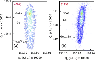
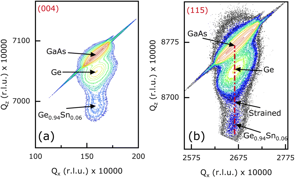
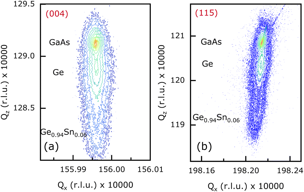
Structural quality and pseudomorphic nature of the epitaxial Ge0.94Sn0.06 layers in samples A1 {(100)/2°}, B1 {(100)/6°}, and C {(110)} were characterized using high-resolution X-ray diffraction (HR-XRD) analysis. Characterization of sample D with (111)A crystal orientation was not performed as it has a low carrier lifetime (discussed below). Reciprocal space maps (RSMs) of each Ge0.94Sn0.06/Ge/GaAs heterostructure material system are shown in Fig. 2–4 (samples A1, B1, and C). This was recorded using PANalytical X-pert Pro system equipped with PIXcel and proportional detectors. The reciprocal lattice point (RLP) of each layer is shown in these figures. Qz-separation between the RLP contours of Ge0.94Sn0.06, Ge, and (100)/2° GaAs substrate, shown in symmetric (004) RSM of Fig. 2(a), confirms different out-of-plane lattice constants of each layer, whereas their Qx alignment shows that they have same in-plane lattice constants. Ge0.94Sn0.06 RLP contour in the bottom part of the figure depicts a larger separation between the (004) planes than in the Ge epilayer. Despite epitaxial Ge being a thinner layer than Ge0.94Sn0.06, Ge RLP contours have higher intensity due to its lattice parameters matching closely to the GaAs substrate with cubic crystal structure, whereas Ge0.94Sn0.06 layer is compressively strained with tetragonal crystal structure. The alignment of Qz along the same line in both (004) and (115) {see Fig. 2(b)} RSMs shows that the Ge0.94Sn0.06 epitaxial layer is compressively strained on Ge layer and GaAs substrate, representing its pseudomorphic nature. The narrow RSMs confirm the good crystalline quality of the epitaxial layer.16 Similar observations can be noted for the 100 nm thick pseudomorphic Ge0.94Sn0.06 epitaxial layer grown on 27 nm Ge layer on a (100)/6° GaAs substrate, as shown in Fig. 3. It is also observed that the Ge0.94Sn0.06 RLPs in both the (100)/2° and (100)/6° samples are symmetric, a quality exhibiting crystalline nature. However, note that the diffraction intensity of the Ge0.94Sn0.06 RLP in (100)/2° is higher than (100)/6°. This does not hold a relation with regards to the quality of the epitaxial layers in comparison to samples A1 and B1. It is reported that the (004) RSM has a higher intensity for the less misoriented substrates, especially for GaAs50 by experiment and simulation. Our results reported here are conclusive evidence of GeSn sample with higher intensity on (100)/2° than (100)/6° orientation. Thus, there is no correlation between the relative intensity of the RSMs with substrate misorientation. Similar conclusions can be drawn from the RSM of sample C, shown in Fig. 4, where 100 nm Ge0.94Sn0.06 was grown on 27 nm Ge over (110) GaAs substrate. Note that the in-plane strain is in the (110) plane (not the (004) plane), leading to no strain calculation from the X-ray analysis. To further analyze the material quality of these epitaxial Ge0.94Sn0.06 layers, carrier lifetimes were measured using μ-PCD technique.
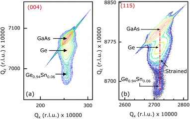 |
| | Fig. 2 Reciprocal space maps (RSMs) taken along the (a) (004) and (b) (115) orientations, that shows ∼0.81% compressive strain in the 100 nm thick Ge0.94Sn0.06 epitaxial layer (sample A1) grown on 27 nm Ge/(100)/2° GaAs substrate. | |
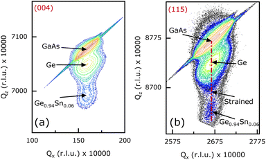 |
| | Fig. 3 Reciprocal space maps (RSMs) taken along the (a) (004) and (b) (115) orientations, that shows ∼0.81% compressive strain in the 100 nm thick Ge0.94Sn0.06 epitaxial layer (sample B1) grown on 27 nm Ge layer/(100)/6° GaAs substrate. | |
 |
| | Fig. 4 Reciprocal space maps (RSMs) taken along the (a) (004) and (b) (115) orientations show 100 nm thick Ge0.94Sn0.06 epitaxial layer (sample C) grown on 27 nm Ge layer/(110) GaAs substrate. | |
3.2. Heterostructure analysis via TEM
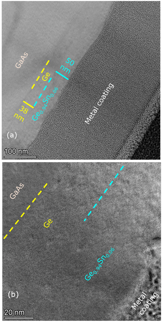
Cross-sectional TEM measurement and analysis of a representative Ge0.94Sn0.06/Ge/GaAs(100)/2° heterostructure sample A2 (similar to samples A1–D), was performed. Fig. 5(a) displays a low-resolution TEM micrograph showing a 50 nm epitaxial Ge0.94Sn0.06 on a 38 nm thick Ge grown over a (100)/2° GaAs substrate. Note that the dashed lines demarcating the Ge and Ge0.94Sn0.06 epilayers guide to a very subtle difference in shades of these layers since Ge and Ge0.94Sn0.06 have similar structure factors and atomic scattering amplitudes. Fig. 5(b) depicts a higher resolution TEM micrograph that implicitly confirms smooth, abrupt heterointerface and good crystalline homogeneity. No visible defects or dislocations are observed in this pseudomorphic heterostructure material system due to the in-plane compressive strain within the Ge0.94Sn0.06 epilayer. Hence, the superior structural quality, as evident by both X-ray and TEM analyses, will corroborate the high minority carrier lifetimes of these epitaxial Ge0.94Sn0.06 materials.
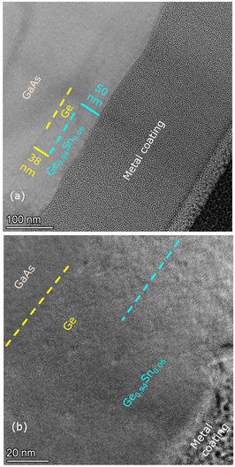 |
| | Fig. 5 Cross-sectional TEM micrographs of sample A2: (a) Ge0.94Sn0.06/Ge/(100)/2° GaAs heterostructure representing good quality growth of 50 nm Ge0.94Sn0.06 grown over 38 nm thick Ge layer grown on GaAs, where broken lines demarcate similar structure factored Ge and Ge0.94Sn0.06 epilayers, and (b) HR-TEM micrograph affirms the fine quality of the GeSn/Ge heterostructure system. | |
3.3. Raman spectroscopic analysis of epitaxial GeSn
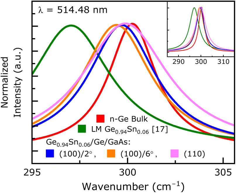
Raman spectroscopy has been widely used by semiconductor industries as well as researchers to analyze the structural and vibrational properties of semiconductor materials for electronic and photonic device applications.42–44,51 When a cubic semiconductor undergoes compressive (tensile) strain due to the underlying stressors, there is invariably a positive (negative) shift observed in the Raman frequencies that denotes the change in vibrational properties (phononic oscillations) of the material under study. This Raman wavenumber shift, Δω together with the material parameter, b, accounts for phononic deformation potential values, and compliance tensor elements that lead to stress-dependent tetragonal distortion in a cubic semiconductor. Unstrained GeSn crystal Raman wavenumber (ω0) is used to calculate the in-plane biaxial strain (ε||) in a crystal lattice using the relation Δω = −b·ε|| cm−1.43,44 Wherein, a widely accepted standard value of b for GeSn material is not available owing to multiple factors elaborated previously that requires decoupling the strain and composition related components.44 One way to address this b value for GeSn has been demonstrated previously by Lin et al.52 for 4.7 ± 0.4% Sn composition, giving b = −563 ± 34 cm−1. In that study, GeSn was grown with varying strains at a fixed Sn composition using different underlying buffer layers, that helped decoupling the composition component involved in the Raman shifts.
In the present work, the amount of compressive strain in epitaxial Ge0.94Sn0.06 layer of sample A1 is calculated using the b value of a lattice matched Ge0.94Sn0.06/In0.12Al0.88As/GaAs(100)/2° heterostructure system, previously demonstrated,17 that has an unstrained crystal lattice of 350 nm Ge0.94Sn0.06 layer in which the measured LO phonon Raman wavenumber was determined as, ω0 = 297.05 ± 0.03 cm−1. The lattice matched Ge0.94Sn0.06 sample referred to above is the same substrate orientation of sample A1 (compressive), enabling us to calculate the biaxial compressive strain. The Raman wavenumber from sample A1 was determined to be ωA1 = 299.71 ± 0.026 cm−1 as shown in Fig. 6, giving ΔωA1 = 2.66 cm−1. Using bGe0.94Sn0.06 = 314.81 ± 14 cm−1 from ref. 17, the in-plane biaxial compressive strain is calculated to be ∼0.84 ± 0.03%, which is in agreement with the strain value of ∼0.81% from X-ray analysis above (Fig. 2). In addition, a new b parameter is required for each orientated sample for calculating strain via Raman measurement. Furthermore, strain-induced phononic oscillations in (100) backscattering geometry split into a singlet LO mode and a doublet transverse optical (TO) mode.53 The Raman shifts on LO mode due to the applied stress from the underlying layer is twice that observed on the TO peak shifts.53 Thus, the strain calculations carried out in this work using the reference sample with (100)/2° orientation cannot be directly applied to the other backscattering geometries like (110) {TO} or (111) {both LO and TO} due to different phononic deformation potential. The orientation dependent strain calculations from Raman spectroscopy in a backscattering geometry are outside the scope of this work due to lattice matched GeSn standard needed for each orientation. Samples A1{(100)/2°}, B2{(100)/6°} and C{(110)} Raman wavenumbers were extracted from Fig. 6 as ωA1 = 299.71 ± 0.026 cm−1, ωB2 = 299.42 ± 0.026 cm−1, and ωC = 299.89 ± 0.036 cm−1, respectively. The full width at half maximum (FWHM) of n-type bulk Ge was 3.26 cm−1 and for samples A1, B2, and C were 4.4 cm−1, 4.31 cm−1, and 5.466 cm−1, respectively, and lower the value better the quality of the sample. Comparing the FWHM of Ge0.94Sn0.06 epitaxial layers grown on oriented GaAs substrates, one can find that the Ge0.94Sn0.06 layer grown on a (100)/6° GaAs exhibits a lower value, which signifies good quality material.
 |
| | Fig. 6 Raman spectra recorded from epitaxial Ge0.94Sn0.06 layers of samples A1, B2 and C (compressively strained heterostructures), selectively chosen with different orientations alongside a lattice matched Ge0.94Sn0.06 epilayer.17 Positive Raman wavenumber shifts (representing compressively strained states) are observed on all three samples A1: (100)/2°, B2: (100)/6°, and C: (110). | |
3.3. Minority carrier lifetime by μ-PCD technique
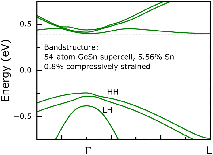
Minority carrier lifetime of a semiconductor continues to be a critical parameter in evaluating the quality of a material. There are several techniques available to determine the lifetime of a carrier, such as time-resolved photoluminescence (TRPL), transient free carrier absorption (TFCA), resonant couple photoconductive decay (RCPCD), μ-PCD, etc.45,54 Here, the minority carrier lifetimes of epitaxial (unintentionally doped n-type) Ge0.94Sn0.06 layers in samples A1 to D {except sample A2, presented in ref. 16} were evaluated using μ-PCD technique at room temperature as a function of excitation wavelengths and laser power, shown in Fig. 8–10. At photon wavelengths of 1500 nm (Eph ≈ 0.83 eV) and 1800 nm (Eph ≈ 0.69 eV), the photogenerated carriers were excited to both L- and Γ-valley conduction bands of epitaxial Ge0.94Sn0.06 layers. These excitation wavelengths excite the carriers to both L- and Γ-valley conduction bands, as shown by electronic band structure using DFT calculations over a 54-atom GeSn supercell configuration with 5.56% Sn in Fig. 7. Generalized gradient approximation (GGA) exchange–correlation functional PBE55 and SG15 pseudopotential56 were used in a linear combination of atomic orbitals (LCAO) basis sets approach with Monkhorst–Pack 3 × 3 × 3 k-point grid. This DFT computation method was calibrated with 54-atom Ge giving direct and indirect band gaps of 0.802 eV and 0.673 eV, respectively. A compressive strain of ∼0.8% was applied using −1.12 GPa stress.1 The fundamental direct (Eg,Γ) and indirect (Eg,L) band gaps were determined to be 0.645 eV and 0.628 eV, respectively, at 300 K, shown in Fig. 7. These values were in close agreement with the band gaps of 0.8% compressively strained Ge0.94Sn0.06/Ge heterostructure reported in the literature.7,57 Note that there are accuracy limitations in the energy band gaps determined using DFT, nevertheless 1500 nm and 1800 nm wavelengths will excite carriers to L- and Γ-valley.
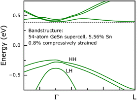 |
| | Fig. 7 Electronic band structure of a 54-atom GeSn supercell with 5.56% Sn, and 0.8% compressive strain. Computed using GGA. PBE exchange–correlation and SG15 pseudopotential in Synopsys QuantumATK tool, the direct, Eg,Γ = 0.645 eV and indirect Eg,L = 0.628 eV band gap values at 300 K are accurate to the limitations of the DFT method employed. Correlating to 1500 nm (Eph = 0.83 eV) and 1800 nm (Eph = 0.69 eV) excitation wavelengths, the photogenerated carriers are excited to the Γ- and L-valleys. | |
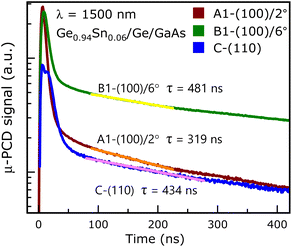 |
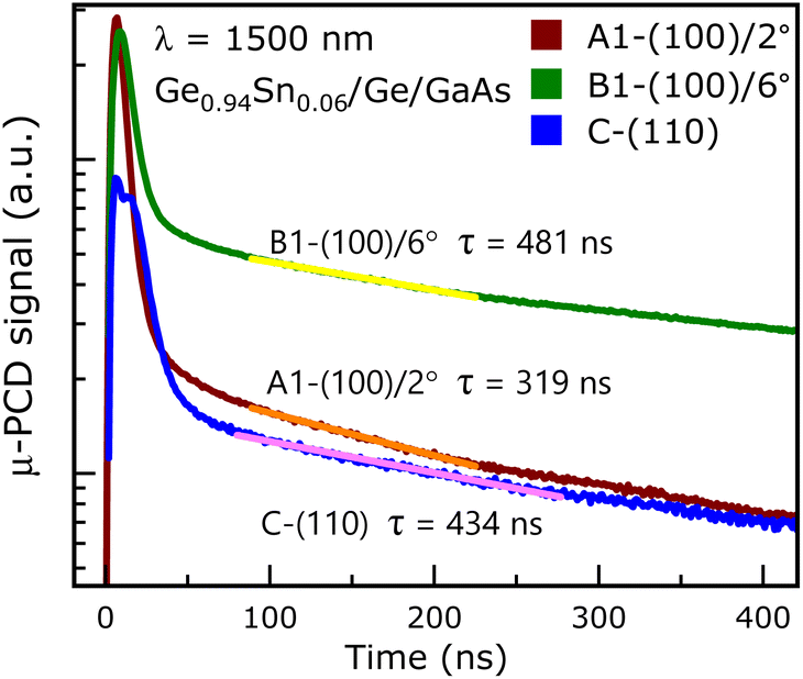
| | Fig. 8 μ-PCD signal versus time acquired at 300 K with 1500 nm excitation wavelength from samples A1 [(100)/2° Ge0.94Sn0.06], B1 [(100)/6° Ge0.94Sn0.06] and C [(110) Ge0.94Sn0.06]. The corresponding minority carrier lifetimes of ∼319 ns, ∼481 ns and ∼434 ns were obtained by fitting to exponential decay after the initial surface recombination induced decay. | |
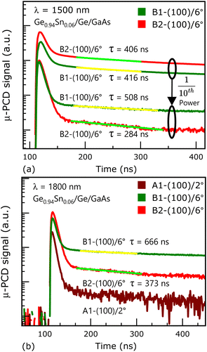 |
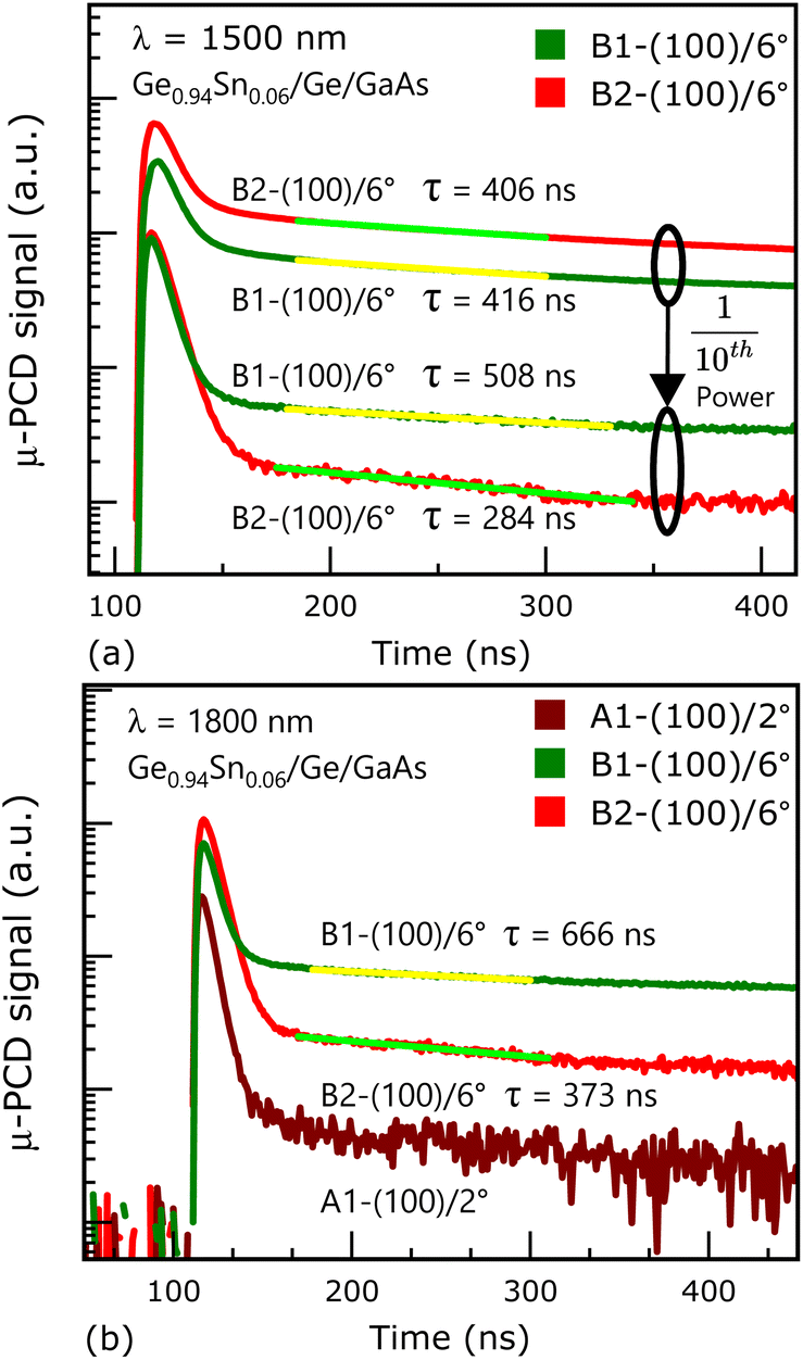
| | Fig. 9 μ-PCD measurement data acquired from (100)/6° Ge0.94Sn0.06 samples B1 and B2 at 300 K using: (a) 1500 nm excitation wavelength with an order of difference in excitation power; (b) 1800 nm excitation wavelength, where sample A1 is also shown. The minority carrier lifetimes obtained for sample B1 (100 nm thick epilayer was grown at 185/150 °C) is higher than sample B2 (50 nm thick epilayer was grown at 225 °C) at both excitation wavelengths, due to thickness and growth temperature.16 It is observed that for sample A1 (100)/2°, the signal is too noisy to extract the lifetime further indicating that (100)/6° orientation offers better quality growth of GeSn epitaxy. | |
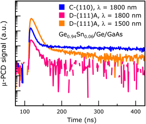 |
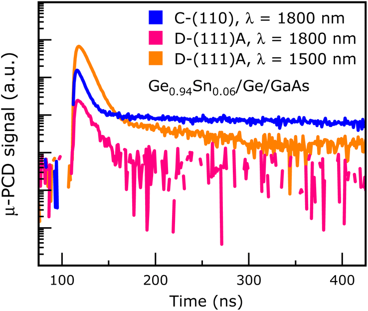
| | Fig. 10 μ-PCD measurement data acquired with 1800 nm excitation wavelength for samples C-(110) and D-(111)A. High surface recombination induced noisy signals make the curve inconducive to single exponential fit, with R2 fitting parameter reaching only 0.41 with 1 as the perfect fit. Similar results are observed at 1500 nm for D-(111)A orientation, indicating its high electrical conductivity, irrespective of excitation wavelength. | |
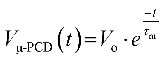
The photogenerated carriers undergo surface states induced carrier recombination prior to their diffusion (deeper) into the bulk-like epitaxial region of the sample. This surface recombination is evident from the fast initial decay below 50 ns (see Fig. 8). The higher energy photons (here, 1500 nm) have stronger absorption, and this photoexcitation leads to a different initial excess carrier distribution where more carriers are generated near the surface. This would lead to more surface recombination and a decay curve more dominated by the initial steep decay. The rate of diffusion towards the bulk region is impacted by the excess carriers remaining after the initial surface recombination, i.e., high surface recombination is related to a high diffusion rate, which gives rise to low minority carrier lifetimes. The minority carrier lifetimes were extracted from the μ-PCD versus time decay curve by fitting the curve to the single exponential decay function  , after the initial surface recombination related fast decay component, where τm is the minority carrier lifetime and Vo is a constant related to the μ-PCD signal's peak intensity. A carrier lifetime value extracted from deep into the μ-PCD signal intensity represents the bulk carrier lifetime, which is higher than an effective carrier lifetime that takes into account the initial decay and diffusion from the near-surface region of the sample.
The μ-PCD lifetimes for the Ge0.94Sn0.06/Ge/GaAs heterostructure samples: A1-(100)/2°, B1-(100)/6° and C (110) were extracted to be 319 ns, 481 ns and 434 ns, respectively, at 1500 nm excitation wavelength, as shown in Fig. 8. The sample surfaces were irradiated by photon fluence of ∼1 × 10⁸ photons per cm2 per pulse, where the associated photoconductivity was recorded 3 ns after 10 pulses per second (each 5 ns wide) were impinged on the sample surface. The μ-PCD signal from sample B1 shows less surface recombination induced decay than of samples A1 and C, which leads to more photogenerated carriers available to diffuse deep into sample B1. Thus, with less rate of diffusion, more carriers are available for conduction before they are lost by recombination and hence high carrier lifetime is obtained from sample B1. The reason behind (100)/6° oriented sample exhibiting a higher carrier lifetime than (100)/2° could be attributed to the reduced charged interface. Whereas the surface of (110) oriented GaAs is nonpolar and has dipoles arranged in a direction parallel to the interface, leading to zero electrostatic potential gradient along the growth direction. This leads to better epitaxy due to thermodynamic stability58–60 at the heterointerface of GeSn/Ge/(100)6° GaAs and GeSn on (110)GaAs substrates. As evident from the literature,61 even a 0.37° offcut in the substrate gives rise to effective thermal stability during an atom-by-atom growth by MBE.
To further verify the effect of misorientation in the (100)/6° GeSn epitaxial layer on the minority carrier lifetimes, the μ-PCD experiment was carried out with two fluences at 1500 nm excitation wavelength, and at a fixed fluence at 1800 nm. The carrier lifetimes and related parameters are summarized in Table 2. Such an experimental result further substantiates the positive effect of 6° offcut on the superior quality of the epitaxial Ge0.94Sn0.06. Samples B1 and B2 showed μ-PCD lifetimes of 406 ns and 416 ns at a fluence of ∼1.8 × 10⁸ photons per cm2 per pulse and 284 ns and 508 ns at a fluence of ∼1 × 10⁷ photons per cm2 per pulse, at 1500 nm wavelength excitation, respectively, as shown in Fig. 9(a). Whereas the same samples have μ-PCD lifetimes of 373 ns and 666 ns with 1800 nm excitation at a fluence of ∼1 × 10⁸ photons per cm2 per pulse, as shown in Fig. 9(b). Sample B1 has a 100 nm Ge0.94Sn0.06 layer, whereas it is 50 nm in B2, the thickness dependent lifetime increase is notable here. This increase in lifetime is due to both the thickness and the growth temperature, as shown in Table 1. However, μ-PCD signal from sample A1 {(100)/2°}, shown in Fig. 9(b) for 1800 nm excitation has high surface recombination (more than other samples) and the signal was too noisy to extract lifetime. The fitting parameter (R2), also known as the coefficient of determination, near 1 gives a mathematical fit with perfect closeness to a long single exponential tail. Low excitation power gives rise to carrier excitations to the lower states of the L- and Γ-valleys of conduction band2 leading to the mathematical fitting away from the perfect R2 values achieved for the high fluence or excitation power. Also, optical excitations closer to the energy band gap of a semiconductor have higher lifetimes.2 At longer excitation wavelengths (here, 1800 nm), photons undergo weaker absorption, and since the epitaxial GeSn layers are thin, the initial excess carrier profile is more uniform, and the carriers near the surface recombine leaving carriers deeper into the bulk to dominate the μ-PCD signal later.
Table 2 Minority carrier lifetimes of epitaxial Ge0.94Sn0.06 layers grown with different orientation and misorientations using microwave-reflection photoconductive decay (μ-PCD) technique
| Sample |
GaAs Substrate |
Ge0.94Sn0.06 thickness (nm) |
Excitation wavelength (nm) |
∼Photon fluence (photons per cm2) per pulse |
μ-PCD lifetime (ns) |
Adj. R2 (fitting) |
| A1 |
(100)/2° |
100 |
1500 |
1 × 10⁸ |
319 |
0.9947 |
| B1 |
(100)/6° |
100 |
481 |
0.9966 |
| C |
(110) |
100 |
434 |
0.9848 |
| B1 |
(100)/6° |
100 |
1.8 × 10⁸ |
406 |
0.997 |
| B2 |
50 |
416 |
0.9946 |
| B1 |
(100)/6° |
100 |
1 × 10⁷ |
284 |
0.9177 |
| B2 |
50 |
508 |
0.9512 |
| B1 |
(100)/6° |
100 |
1800 |
1 × 10⁸ |
373 |
0.9018 |
| B2 |
50 |
666 |
0.9606 |
To observe the effects of (111)A orientation, μ-PCD lifetime of sample D was measured, as shown in Fig. 10, at 1500 nm and 1800 nm excitation wavelengths. It is clear that, irrespective of the wavelength of excitation, the GeSn layer on (111)A GaAs surface orientation exhibits poor photoconductivity, and the μ-PCD signal decays faster than other orientations in the same time windows. This could be attributed to high electrical conductivity.19,21 This effect is widely noted for epitaxial Ge on (111)A GaAs with and without surface passivation,23 possibly ruling out the use of (111)A oriented epitaxial GeSn active layer in optoelectronics.
Nevertheless, the considerable aspect here is that the (100) oriented epitaxial GeSn samples that were grown on 6° offcut (100)GaAs substrates have superior minority carrier lifetimes even at a reduced fluence by 1 order and a long wavelength of 1800 nm excitation. One could achieve a 2-fold benefit while synthesizing a device-quality GeSn epitaxial material on a III–V buffer layer by using misoriented (100)/6° substrates: (i) mitigation of electrostatic potential gradient near the non-polar on polar interface;24,58–60 and (ii) annihilation of APDs at the polar on non-polar interface;24,58–60 both giving the much-needed radiative recombination enhancements in optical applications. The thermodynamic stability comparison between (100)/2° and (100)/6° orientations is presented in the next section with the help of interatomic potential model-based atomistic simulation to elucidate the difference in formation energy and stability of Ge on misoriented GaAs substrates, which explains different carrier lifetimes on (100)/2° and (100)/6° substrates.
3.4. Formation energy computation by atomistic simulation
Atomistic simulation has gained immense popularity and made a huge difference to materials research over the years, as the material properties and parameters at the microscopic scale do not hold level in the atomic scale.41,59 In decreasing order of precision and computation cost involved: quantum chemical calculations, density functional theory, and force field calculations are employed for investigating the atomic level material properties using atomistic simulation.62 In the present work, interatomic potential model-based ATK-ForceField calculations have been carried out on the Ge/GaAs heterointerface with different misorientations, and 6280-atoms in the heterointerface supercell. ZBLStiwePotential is the potential method used in the ATK-ForceField calculator. This is based on the Stillinger–Weber interatomic potential model used for computations in the diamond, zinc blende, and wurtzite crystal semiconductors, where the interatomic bonds are tetrahedral.40 The geometry optimization (also known as energy minimization technique)47,49 is carried out with the maximum force tolerance of 1 meV Å−1. The total energy of the 2-heterointerface structures: (i) Ge-GaAs(100)/2° and (ii) Ge-GaAs(100)/6° were computed to comparatively underscore a more thermodynamically stable system among the two and the formation energy is related as follows:41,63| |  | (1) |
where, Eform is the energy required to dissociate a material into its individual component x, and Etotal is the total energy of the material. For instance, the formation energy of GaAs semiconductor is given as:41,63| | | EGaAsform = EGaAstotal − EGatotal/nGa − EAstotal/nAs | (2) |
where, nGa and nAs are the number of Ga and As atoms in the unit cell.
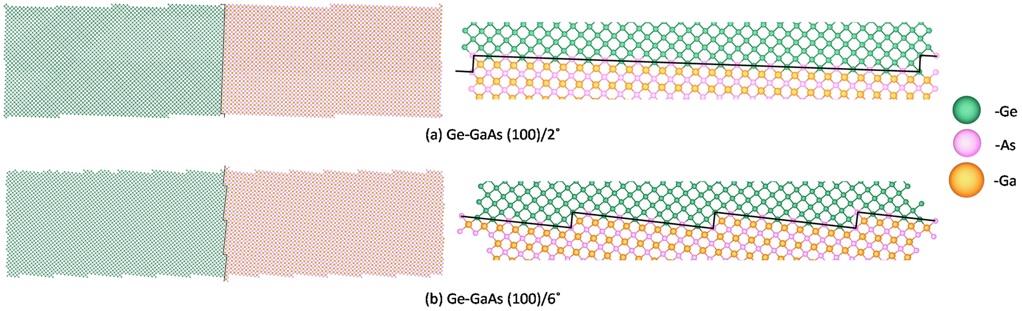
As shown in Fig. 11, both the Ge-GaAs (100)/2° and (100)/6° supercells have 6280-atoms: 3140 Ge-atoms {green}, 1570 Ga-atoms {brown}, and 1570 As-atoms {pink}. The formation energy of each heterointerfacial supercell is derived from its total energy with the rest of the terms on the right-hand side of the equation staying the same for both orientations. As tabulated in Table 3, there are three interfacial bonding environments considered for both Ge-GaAs (100)/6° and Ge-GaAs (100)/2° system: two growth cases where GaAs surface is As-terminated, and one theoretical case where GaAs surface is equally terminated by As- and Ga-atoms. In the first case, shown in Table 3, only Ge–As bonds are present at the interface, making it a charged interface. In the second scenario (theoretical case), there are equal Ge–As and Ge–Ga bonds with no interdiffusion and a neutral interface. Whereas in the third scenario, the GaAs surface is As-terminated with Ge diffused to 1 atomic layer of GaAs making equal number of Ge–Ga and Ge–As bonds, i.e., a neutral interface (as shown in Fig. 11). In all three bonding environment conditions, it is observed that the (100)/6° system has lower total energy and hence lower formation energy. One could attribute this to two reasons: (i) higher density of surface steps on a (100)/6° substrate than the (100)/2° substrate. This is also advantageous as it is widely known that double-stepped surfaces help in the self-annihilation of anti-phase domains24,58–60 when further growth of III–V semiconductor on group IV semiconductor is done; (ii) a smaller number of atoms in the formation of the interfacial supercell, by the CSL method, has been proven to give a thermodynamically stable system. Though this study has been limited to the materials systems having metals, polycrystals, and oxides, however, in the case of semiconductors the nature of the bonding environment makes a significant difference to the thermodynamic stability of the system.48 Herein, by considering the computation of three different bonding environments it was shown that Ge grown on GaAs on the (100)/6° substrate is thermodynamically more stable.
 |
| | Fig. 11 6280-atoms heterointerface supercell of Ge on GaAs (100) surface: (a) misoriented by 2° towards [110] direction having 1 step in 1 unit supercell; (b) misoriented by 6° towards [110] having 3 steps in same sized supercell as (a). It is observed that, both the supercells have double-steps with “As-termination”, however the 6° misorientation has higher density of surface steps than the 2° misorientation substrate, aiding better elimination of antiphase domains when further growth of GaAs will be done on Ge. Note that for the case under consideration here, GaAs heteroepitaxy is As-terminated and the interface is neutral with 1 atomic layer at the interface having alternating Ge and As atoms that form equal number of Ge–As and Ge–Ga bonds to neutralize the charge imbalance at the interface. Schematic drawn using Vesta.64 | |
Table 3 Total Energy of Ge-GaAs heterointerfacial supercell of (100) substrate misoriented by 2° and 6° towards [110] direction with different bonding environments
| Type of heterointerfacial bonding |
Total energy of 6280-atom Ge-GaAs heterointerface supercell (eV) |
Difference in total energy (eV) |
| Bonds |
Interface |
(100)/2° |
(100)/6° |
(100)/2°–(100)/6° |
| #Ge–As |
Charged, no8pt interdiffusion |
3.38 |
1.89 |
1.49 |
| #Ge–Ga = #Ge–As |
Neutral, no8pt interdiffusion |
6.19 |
5.3 |
0.89 |
| #Ge–Ga = #Ge–As |
Neutral, 1 atomic layer interdiffusion |
2.77 |
2.31 |
0.46 |
Further, when Ge0.94Sn0.06 is grown on the (100)/6° system, it has a higher carrier lifetime than on the (100)/2° GaAs substrate. This was observed in 2 separate growths, sample B1 and B2 [both (100)/6°] have 406 ns and 481 ns μ-PCD lifetime, respectively, at 1500 nm excitation, whereas sample A1 [(100)/2°] has μ-PCD lifetime of 319 ns, as discussed in section B. Moreover, when the μ-PCD lifetime measurement was carried out at 1800 nm excitation (i.e., lower energy), it could not excite sufficient carriers to calculate the μ-PCD lifetime in (100)/2° but it was possible in (100)/6°, as shown in Table 2. Hence, one way to overcome the growth challenges faced by epitaxial GeSn materials systems in terms of device quality is to synthesize them on the misoriented substrates that are more thermodynamically stable compared to non-offcut substrates.
4. Conclusions
Tunable tin compositional GeSn materials find applications for silicon-compatible photonics. Extending its reach to further enhance the quantum efficiencies needs synthesizing virtually defect-free and high carrier lifetime GeSn materials. In this work, compressively strained Ge0.94Sn0.06 materials were grown on (100)/2°, (100)/6°, (110), and (111)A GaAs substrates with an intermediate Ge buffer layer by vacuum interconnected solid source molecular beam epitaxy system. High-resolution X-ray analysis displayed 0.81% compressive strain in Ge0.94Sn0.06 layers, which is further corroborated by Raman spectroscopy. In addition, the full width at half maximum of Raman spectral peak from Ge0.94Sn0.06 epitaxial layer on (100)/6° GaAs is smaller than (100)/2° GaAs, indicating superior quality in the former. The defect-free heterointerface of Ge0.94Sn0.06/Ge/GaAs heterostructure was demonstrated by cross-sectional transmission electron microscopy analysis. Minority carrier lifetimes of Ge0.94Sn0.06 epilayers were measured using microwave photoconductive decay technique and displayed high carrier lifetimes of 319 ns (2° offcut) to 481 ns (6° offcut) at 1500 nm excitation wavelength. This carrier lifetime value was enhanced to ∼ 600 ns at 1800 nm excitation wavelength on (100)/6° GaAs substrate. The differences in carrier lifetimes on (100)/6° and (100)/2° GaAs substrates were linked with the formation energy of the Ge/GaAs heterointerface using atomistic simulation with different heterointerfacial bonding. Lower formation energy on (100)/6° is attributed to a higher density of surface steps in 6° and 20× smaller number of atoms in a supercell of 6° by the coincidence site lattice method with different interfacial bonding environments. Total energy computation of 6280-atom Ge/GaAs supercell on (100)/6° leads to lower formation energy (2.31 eV) than (100)2° (2.77 eV), making it more thermodynamically stable. Hence, a misoriented substrate with better thermodynamic stability will aid in realizing device-quality GeSn materials with superior carrier lifetimes, which will boost the performances of optoelectronic devices.
Author contributions
Sengunthar Karthikeyan: conceptualization, data analysis, curation, investigation, visualization, atomistic simulation, writing original draft, review, and editing; Steven W. Johnston: resources, lifetime data collection, investigation, writing – review and editing; Dhammapriy Gayakwad, Suddhasatta Mahapatra: cross-section TEM measurement, review and editing; Robert Bodnar, Jing Zhao: resources, Raman spectroscopy measurement, review and editing; Rutwik Joshi: X-ray measurement, review and editing; Mantu K. Hudait: resources, supervision, project administration, funding acquisition, methodology, analysis, writing – review and editing.
Conflicts of interest
There are no conflicts to declare.
Acknowledgements
M. K. H. and S. K. acknowledge partial support from the NSF under grant number ECCS-2042079, a US-Ireland Joint R&D Program, Virginia Tech Nanofabrication facilities for assistance during materials analysis and A. Laha, SAIF and IRCC (IIT Bombay) for facilitating TEM sample preparation and analysis. S. J acknowledges that the views expressed herein do not necessarily represent the views of the U.S. Department of Energy or the United States Government.
References
-
Photonics and Electronics with Germanium, ed. K. Wada and L. C. Kimerling, Wiley-VCH, 2015 Search PubMed.
-
Silicon Photonics IV Topics in Applied Physics, ed. D. Lockwood and L. Pavesi, Springer Nat., 2021 Search PubMed.
- L. Zhang, A. M. Agarwal, L. C. Kimerling and J. Michel, Nanophotonics, 2014, 3, 247–268 CAS.
- S. Xu, W. Wang, Y.-C. Huang, Y. Dong, S. Masudy-Panah, H. Wang, X. Gong and Y.-C. Yeo, Opt. Express, 2019, 27, 5798–5813 CrossRef PubMed.
- H. Tran, T. Pham, J. Margetis, Y. Zhou, W. Dou, P. Grant, J. M. Grant, S. Al-Kabi, G. Sun, R. A. Soref, J. Tolle, Y.-H. Zhang, W. Du, B. Li, M. Mortazavi and S.-Q. Yu, ACS Photonics, 2019, 6, 2807–2815 CrossRef CAS.
- K.-C. Lee, M.-X. Lin, H. Li, H.-H. Cheng, G. Sun, R. Soref, J. Hendrickson, K.-M. Hung, P. Scajev and A. Medvids, Appl. Phys. Lett., 2020, 117, 012102 CrossRef CAS.
- R. Chen, S. Gupta, Y.-C. Huang, Y. Huo, C. Rudy, E. Sanchez, Y. Kim, T. Kamins, K. C. Saraswat and J. S. Harris, Nano Lett., 2014, 14, 37–43 CrossRef CAS PubMed.
- O. Moutanabbir, S. Assali, X. Gong, E. O'Reilly, C. A. Broderick, B. Marzban, J. Witzens, W. Du, S.-Q. Yu, A. Chelnokov, D. Buca and D. Nam, Appl. Phys. Lett., 2021, 118, 110502 CrossRef CAS.
- C.-Y. Chang, R. Bansal, K.-C. Lee, G. Sun, R. Soref, H. H. Cheng and G.-E. Chang, Opt. Lett., 2021, 46, 3316–3319 CrossRef CAS PubMed.
- D. Rainko, Z. Ikonic, A. Elbaz, N. V. d. Driesch, D. Stange, E. Herth, P. Boucaud, M. E. Kurdi, D. Grützmacher and D. Buca, Sci. Rep., 2019, 9, 259 CrossRef PubMed.
- J. Liu, X. Sun, D. Pan, X. Wang, L. C. Kimerling, T. L. Koch and J. Michel, Opt. Express, 2007, 15, 11272 CrossRef CAS PubMed.
- G. Sun, R. A. Soref, J. Khurgin, S.-Q. Yu and G.-E. Chang, Opt. Express, 2022, 30, 42385–42393 CrossRef CAS PubMed.
- R. Douhan, K. Lozovoy, A. Kokhanenko, H. Deeb, V. Dirko and K. Khomyakova, Technology, 2023, 11, 17 Search PubMed.
- M. Li, J. Zheng, X. Liu, Y. Zhu, C. Niu, Y. Pang, Z. Liu, Y. Zuo and B. Cheng, Appl. Phys. Lett., 2022, 120, 121103 CrossRef CAS.
- A. N. Lemire, K. A. Grossklaus and T. Vandervelde, J. Vac. Sci. Technol., 2023, 41, 052701 CrossRef CAS.
- M. K. Hudait, S. W. Johnston, M. B. Clavel, S. Bhattacharya, S. Karthikeyan and R. Joshi, J. Mater. Chem. C, 2022, 10, 10530–10540 RSC.
- S. Karthikeyan, R. Joshi, J. Zhao, R. J. Bodnar, B. A. Magill, Y. Pleimling, G. A. Khodaparast and M. K. Hudait, J. Mater. Chem. C, 2023, 11, 9472–9485 RSC.
- J. S. Harris, H. Lin, R. Chen, Y. Huo, E. Fei, S. Paik, S. Cho and T. Kamins, ECS Trans., 2012, 50, 601 CrossRef.
- C.-S. Tan, M.-Y. Lu, W.-H. Peng, L.-J. Chen and M. H. Huang, J. Phys. Chem. C, 2020, 124, 13304 CrossRef CAS.
- K. Alam, S. Takagi and M. Takenaka, IEEE Trans. Electron Devices, 2014, 61, 3594–3600 CAS.
- C.-S. Tan, Y. Zhao, R.-H. Guo, W.-T. Chuang, L.-J. Chen and M. H. Huang, Nano Lett., 2020, 20, 1952 CrossRef CAS PubMed.
- M. K. Hudait and S. W. Johnston, Mater. Adv., 2022, 3, 5034–5042 RSC.
- M. K. Hudait, S. W. Johnston, M. R. Das, S. Karthikeyan, P. P. Sahu, J. Das, J. Zhao, R. J. Bodnar and R. Joshi, ACS Appl. Electron. Mater., 2023, 5, 3350 CrossRef CAS.
- M. K. Hudait, Y. Zhu, N. Jain and J. L. Hunter Jr., J. Vac. Sci. Technol., B: Nanotechnol. Microelectron.: Mater., Process., Meas., Phenom., 2013, 31, 011206 Search PubMed.
- M. K. Hudait and Y. Zhu, J. Appl. Phys., 2013, 113, 114303 CrossRef.
- M. K. Hudait, Y. Zhu, D. Maurya, S. Priya, P. K. Patra, A. W. K. Ma, A. Aphale and I. Macwan, J. Appl. Phys., 2013, 113, 134311 CrossRef.
- P. D. Nguyen, M. B. Clavel, J.-S. Liu and M. K. Hudait, IEEE Trans. Electron Devices, 2017, 64, 4457 CAS.
- P. D. Nguyen, M. B. Clavel, A. Ghosh and M. K. Hudait, Microelectron. Eng., 2018, 199, 80–86 CrossRef CAS.
- Y.-S. Wu and P. Su, IEEE Trans. Electron Devices, 2010, 57, 3312–3317 CAS.
- Y.-S. Wu, M.-L. Fan and P. Su, Silicon Nanoelectron. Workshop, 2010, 1–2 Search PubMed.
- C. D. Young, K. Akarvardar, M. O. Baykan, K. Matthews, I. Ok, T. Ngai, K.-W. Ang, J. Pater, C. E. Smith, M. M. Hussain, P. Majhi and C. Hobbs, Solid State Electrochem., 2012, 78, 2–10 CrossRef CAS.
- R. Joshi, S. Karthikeyan and M. K. Hudait, IEEE Trans. Electron Devices, 2022, 69, 4175–4182 CAS.
- P. Ye, T. Ernst and M. Khare, IEEE Spectrum, 2019, 56, 30 Search PubMed.
- E. Capogreco, L. Witters, H. Arimura, F. Sebaai, C. Porret, A. Hikavyy, R. Loo, A. P. Milenin, G. Eneman, P. Favia, H. Bender, K. Wostyn, E. D. Litta, A. Schulze, C. Vrancken, A. Opdebeeck, J. Mitard, R. Langer, F. Holsteyns, N. Waldron, K. Barla, V. De Heyn, D. Mocuta and N. Collaert, IEEE Trans. Electron Devices, 2018, 65, 5145–5150 CAS.
- D. Nagy, G. Indalecio, A. J. GarcíA-Loureiro, M. A. Elmessary, K. Kalna and N. Seoane, IEEE Trans. Electron Devices, 2018, 6, 332–340 CAS.
- R. Joshi, S. Karthikeyan and M. K. Hudait, IEEE Trans. Electron Devices, 2023, 70, 899–907 CAS.
- K. H. Lee, Y. H. Tan, A. Jandl, E. A. Fitzgerald and C. S. Tan, J. Electron. Mater., 2013, 42, 1133–1139 CrossRef CAS.
- G. B. Galiev, I. S. Vasil'evskii, E. A. Klimov, S. S. Pushkarev, A. N. Klochkov, P. P. Maltsev, M. Yu. Presniakov, I. N. Trunkin and A. L. Vasiliev, J. Cryst. Growth, 2014, 392, 11–19 CrossRef CAS.
- R. S. Goldman, K. Kavanagh, H. Wieder, S. Ehrlich and R. M. Feenstra, J. Appl. Phys., 1998, 83, 5137 CrossRef CAS.
- F. H. Stillinger and T. A. Weber, Phys. Rev. B: Condens. Matter Mater. Phys., 1985, 31, 5262 CrossRef CAS PubMed.
- QuantumATK version U-2022.12-SP1, Synopsys. https://www.synopsys.com/silicon/quantumatk.html.
- W. S. Yoo, H. Harima and M. Yoshimoto, ECS J. Solid State Sci. Technol., 2015, 4, 356 CrossRef.
- C.-Y. Peng, C.-F. Huang, Y.-C. Fu, Y.-H. Yang, C.-Y. Lai, S.-T. Chang and C. W. Liu, J. Appl. Phys., 2009, 105, 083537 CrossRef.
- C. Chang, H. Li, T.-P. Chen, W.-K. Tseng, H. Cheng, C.-T. Ko, C.-Y. Hsieh, M.-J. Chen and G. Sun, Thin Solid Films, 2015, 593, 40–43 CrossRef CAS.
- S. Johnston, K. Zaunbrecher, R. Ahrenkiel, D. Kuciauskas, D. Albin and W. Metzger, IEEE Photovoltaic, 2014, 4, 1295–1300 Search PubMed.
- M. A. Fortes, Phys. Status Solidi B, 1972, 54, 311–319 CrossRef CAS.
- D. Stradi, L. Jelver, S. Smidstrup and K. Stokbro, J. Phys.: Condens. Matter, 2017, 29, 185901 CrossRef PubMed.
- D. Brandon, Mater. Sci. Technol., 2010, 26, 762–773 CrossRef CAS.
- J. Schneider, J. Hamaekers, S. T. Chill, S. Smidstrup, J. Bulin, R. Thesen, A. Blom and K. Stokbro, Modell. Simul. Mater. Sci. Eng., 2017, 25, 085007 CrossRef.
- L. Zhiwei, Y. Zeng, Y. Song, J. Zhang, Y. Zhou, Y. Ning, L. Qin and L. Wang, Appl. Sci., 2021, 11, 8639 CrossRef.
- J. H. Parker Jr., D. W. Feldman and M. Ashkin, Phys. Rev., 1967, 155, 712 CrossRef.
- H. Lin, R. Chen, Y. Huo, T. I. Kamins and J. S. Harris, Appl. Phys. Lett., 2011, 98, 261917 CrossRef.
-
E. Anastassakis and M. Cardona, High Pressure in Semiconductor Physics II, Academic Press, San Diego, CA, 1998, ch. 3, p. 55 Search PubMed.
- S. Johnston, R. Ahrenkiel, P. Dippo, Matt Page and Wyatt Metzger, MRS Online Proc. Libr., 2006, 994, 09940704 CrossRef.
- W. Kohn and L. J. Sham, Phys. Rev., 1965, 140, A1133 CrossRef.
- S. Smidstrup, D. Stradi, J. Wellendorff, P. A. Khomyakov, U. G. Vej-Hansen, M. E. Lee, T. Ghosh, E. Jónsson, H. Jónsson and K. Stokbro, Phys. Rev. B, 2017, 96, 195309 CrossRef.
- A. A. Tonkikh, C. Eisenschmidt, V. G. Talalaev, N. D. Zakharov, J. Schilling, G. Schmidt and P. Werner, Appl. Phys. Lett., 2013, 103, 032106 CrossRef.
- W. A. Harrison, E. A. Kraut, J. R. Waldrop and R. W. Grant, Phys. Rev. B: Condens. Matter Mater. Phys., 1978, 18, 4402 CrossRef CAS.
- W. E. Pickett, S. G. Louie and M. L. Cohen, Phys. Rev. B: Condens. Matter Mater. Phys., 1978, 17, 815 CrossRef CAS.
- R. W. Grant, J. R. Waldrop and E. A. Kraut, Phys. Rev. Lett., 1978, 40, 656 CrossRef CAS.
- P. R. Pukite, J. M. Van Hove and P. I. Cohen, J. Vac. Sci. Technol., B: Microelectron. Process. Phenom., 1984, 2, 243–248 CrossRef CAS.
- S. Smidstrup, T. Markussen, P. Vancraeyveld, J. Wellendorff, J. Schneider, T. Gunst, B. Verstichel, D. Stradi, P. A. Khomyakov, U. G. Vej-Hansen, M.-E. Lee, S. T. Chill, F. Rasmussen, G. Penazzi, F. Corsetti, A. Ojanperä, K. Jensen, M. L. N. Palsgaard, U. Martinez, A. Blom, M. Brandbyge and K. Stokbro, J. Phys.: Condens. Matter, 2020, 32, 015901 CrossRef CAS PubMed.
- F. El-Mellouhi and N. Mousseau, Phys. Rev. B: Condens. Matter Mater. Phys., 2005, 71, 125207 CrossRef.
- K. Momma and F. Izumi, J. Appl. Crystallogr., 2011, 44, 1272–1276 CrossRef CAS.
|
| This journal is © The Royal Society of Chemistry 2024 |
Click here to see how this site uses Cookies. View our privacy policy here. 
 Open Access Article
 This Open Access Article is licensed under a Creative Commons Attribution-Non Commercial 3.0 Unported Licence
 a,
Steven W.
Johnston
a,
Steven W.
Johnston

 , after the initial surface recombination related fast decay component, where τm is the minority carrier lifetime and Vo is a constant related to the μ-PCD signal's peak intensity. A carrier lifetime value extracted from deep into the μ-PCD signal intensity represents the bulk carrier lifetime, which is higher than an effective carrier lifetime that takes into account the initial decay and diffusion from the near-surface region of the sample.