
 Open Access Article
 This Open Access Article is licensed under a
 Creative Commons Attribution 3.0 Unported Licence
Optical spectroscopic detection of Schottky barrier height at a two-dimensional transition-metal dichalcogenide/metal interface†
Du
Chen
 ab,
Surendra B.
Anantharaman
c,
Jinyuan
Wu
bd,
Diana Y.
Qiu
bd,
Deep
Jariwala
c and
Peijun
Guo
*ab
ab,
Surendra B.
Anantharaman
c,
Jinyuan
Wu
bd,
Diana Y.
Qiu
bd,
Deep
Jariwala
c and
Peijun
Guo
*ab
aDepartment of Chemical and Environmental Engineering, Yale University, New Haven, CT 06520, USA. E-mail: peijun.guo@yale.edu
bEnergy Sciences Institute, Yale University, West Haven, CT 06516, USA
cDepartment of Electrical and Systems Engineering, University of Pennsylvania, Philadelphia, PA 19104, USA
dDepartment of Mechanical Engineering and Materials Science, Yale University, New Haven, CT 06520, USA
First published on 23rd February 2024
Abstract
Atomically thin two-dimensional transition-metal dichalcogenides (2D-TMDs) have emerged as semiconductors for next-generation nanoelectronics. As 2D-TMD-based devices typically utilize metals as the contacts, it is crucial to understand the properties of the 2D-TMD/metal interface, including the characteristics of the Schottky barriers formed at the semiconductor-metal junction. Conventional methods for investigating the Schottky barrier height (SBH) at these interfaces predominantly rely on contact-based electrical measurements with complex gating structures. In this study, we introduce an all-optical approach for non-contact measurement of the SBH, utilizing high-quality WS2/Au heterostructures as a model system. Our approach employs a below-bandgap pump to excite hot carriers from the gold into WS2 with varying thicknesses. By monitoring the resultant carrier density changes within the WS2 layers with a broadband probe, we traced the dynamics and magnitude of charge transfer across the interface. A systematic sweep of the pump wavelength enables us to determine the SBH values and unveil an inverse relationship between the SBH and the thickness of the WS2 layers. First-principles calculations reveal the correlation between the probability of injection and the density of states near the conduction band minimum of WS2. The versatile optical methodology for probing TMD/metal interfaces can shed light on the intricate charge transfer characteristics within various 2D heterostructures, facilitating the development of more efficient and scalable nano-electronic and optoelectronic technologies.
 Peijun Guo | Peijun Guo received his B.S. from Tsinghua University and his M.S. and Ph.D. from Northwestern University, all in Materials Science and Engineering. After spending three years at Argonne National Laboratory as an Enrico Fermi Named Postdoc Fellow, he joined the Department of Chemical and Environmental Engineering at Yale University in the year 2020, and he is also an affiliated faculty member at the Energy Sciences Institute. He has authored and coauthored more than 90 peer-reviewed journal publications and has been recognized with the Materials Research Society Graduate Student Gold Award, the SPIE Education Scholarship, and the AFOSR Young Investigator Award. His research is focused on the design and synthesis of inorganic and hybrid materials for enhanced light–matter interactions, and time-resolved optical studies of excited-state dynamics in complex material systems for energy conversion, optoelectronics, and information science. |
Introduction
Transition metal dichalcogenides (TMDs) are a family of emerging two-dimensional (2D) materials featuring many attractive properties. Compared with previously well-established 2D materials like graphene and hexagonal boron nitride (h-BN), the presence of appropriate band gaps in TMDs make them promising candidates for various electronic and optoelectronic applications, such as field-effect transistors,1,2 valleytronics,3,4 photodetectors,5–7 photovoltaics,8,9 and light-emitting diodes.10–13 One common issue limiting the performance of these applications is the contact resistance at the TMD-metal interface,14,15 which mainly originates from the Schottky barrier formed between the TMDs and metals.16,17The formation of the Schottky barrier is primarily attributed to the energy band alignments between the TMDs and metals,14 and metal-induced gap states.18 A minimal or even zero Schottky barrier height (SBH) is favorable in most applications. Although many theoretical studies and calculations are available,19–22 experimental measurements of the SBH often require complex gated-transistor structures,18,23–25 or specialized atomic force microscopies.14,15,26 The extraction of SBH by the above-mentioned methods is based on the electrical I–V curve or contact potential measurement. Here, we demonstrate an optical, pump–probe spectroscopy-based approach to achieve non-contact measurement of the SBH, using WS2–Au interface as a model system.
Gold is one of the most widely used electrode materials and is known to form a Schottky contact with sulfide-based TMDs, e.g., MoS2 and WS2,14,24,27,28 since gold has a work function of approximately 5.3 eV,29 exceeding the electron affinity of WS2 (∼4.5 eV).30 This energy difference leads to an SBH of approximately 0.8 eV. In a heterostructure formed by WS2 and gold, electrons in the gold experience a potential barrier and are hindered from flowing into the WS2. It has been reported that light can excite electrons with energies large enough to overcome the barrier and be injected into the WS2, which then form excitons or recombine with the intrinsic holes within the WS2.28,31 In this paper, we employ near-infrared (NIR) pump that lies below the bandgap of WS2 to induce hot-electron injection from gold to WS2. Owing to the strong absorption bleaching by photoexcited free carriers and excitons,32 a broadband probe is applied to monitor the carrier populations within the WS2. By sweeping the energy of the pump photons, we observe certain thresholds, below which the energy of the pump photon is insufficient to induce significant amount of electron injection into WS2, permitting the extraction of the SBH. Our work demonstrates an alternative, all-optical, non-contact method to measure the SBH between TMDs and metals, and sheds light into the electron transport channels at the TMD-metal interface.
Results and discussion
We mechanically exfoliated monolayer and few-layer WS2 onto smooth gold substrates (see Fig. S1a†). The thickness of the flakes was determined using atomic force microscopy (AFM), revealing layer numbers of 1, 5, and 10 (see Fig. S1b†), assuming a monolayer thickness of 0.6 nm.33 Pump–probe transient reflection (TR) experiments were carried out on these samples under ambient conditions. We utilized an optical objective to focus probe pulses onto the sample with a sub-5 μm spot size. The pump source, ranging from 1100 nm (1.12 eV) to 2700 nm (0.46 eV), was generated using an optical parametric amplifier (OPA) powered by a Pharos amplifier. The Pharos amplifier produces a fundamental output wavelength of 1030 nm and a pulse duration of 170 fs at a repetition rate of 2 kHz. Supercontinuum probe pulses (530–720 nm) were generated by focusing a small portion of the 1030 nm fundamental output onto a 4-mm thick YAG crystal (see Fig. S2†). Steady-state optical reflectance was measured using the same pump–probe microscopy setup, with the pump light turned off. All the optical measurements were performed at ambient conditions.We observed two distinct resonant dips in the reflectance spectra (Fig. 1a), corresponding to the A and B excitons in WS2 at the K point. These resonant dips display a redshift with increasing layer number, consistent with findings from a previous band-structure study on WS2.34 The TR experimental results for a 1L-WS2/Au sample under 400 nm excitation are presented in Fig. 1b, expressed in terms of ΔR/R. Here, ΔR/R is defined as [R(t) − R(0)/R(0)], where R(0) represents the reflectance without pump excitation, and R(t) is the reflectance at delay time t after the pump excitation. The kinetics of ΔR/R extracted at the resonant dip wavelength, as shown in Fig. 1b, exhibits a typical photobleaching response. This suggests the rapid formation of free electron–hole pairs within the first 500 fs, followed by the creation of excitons from thermally equilibrated hot carriers.35 The TR results distill a high sensitivity of reflectance to an excess density of charge carriers and excitons, indicating the possibility for detecting additional charge carriers injected from gold to WS2 when overcoming the Schottky barrier.
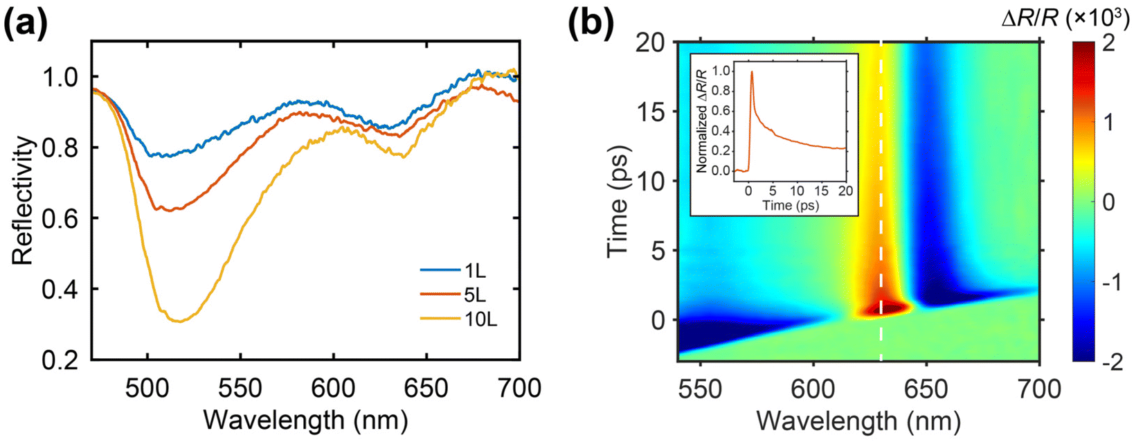 | ||
| Fig. 1 (a) Steady-state reflectance spectra of 1L, 5L and 10L-WS2 on gold; the reflectance were normalized by the gold substrate. (b) Transient ΔR/R spectral map of 1L-WS2/Au excited by above-bandgap pump with a wavelength of 400 nm. Note that the chirp of the TR data hasn't been corrected, which however doesn't change the conclusion. The inset shows the kinetics of ΔR/R extracted at 640 nm, corresponding to the positive peak of photon bleaching features (indicated by the white-dashed line in the figure). | ||
We then performed TR experiments on both an Au/glass sample and the 1L-WS2/Au/glass sample using a pump wavelength of 1100 nm, and the resulting transient spectral maps of ΔR/R are shown in Fig. 2a and b, respectively. The pump photon energy of approximately 1.1 eV is notably below the bandgap of WS2.34 In Fig. 2a, a robust and broad transient ΔR/R signal is observed on the bare gold film. Fig. 2b presents the ΔR/R transient spectral map collected on the 1L-WS2/Au sample. Notably, the ΔR/R comprises a broadband bleaching response consistent with the TR result obtained from gold, along with a prominent positive lobe of ΔR/R centered at approximately 642 nm, corresponding to the WS2 A-exciton resonance.
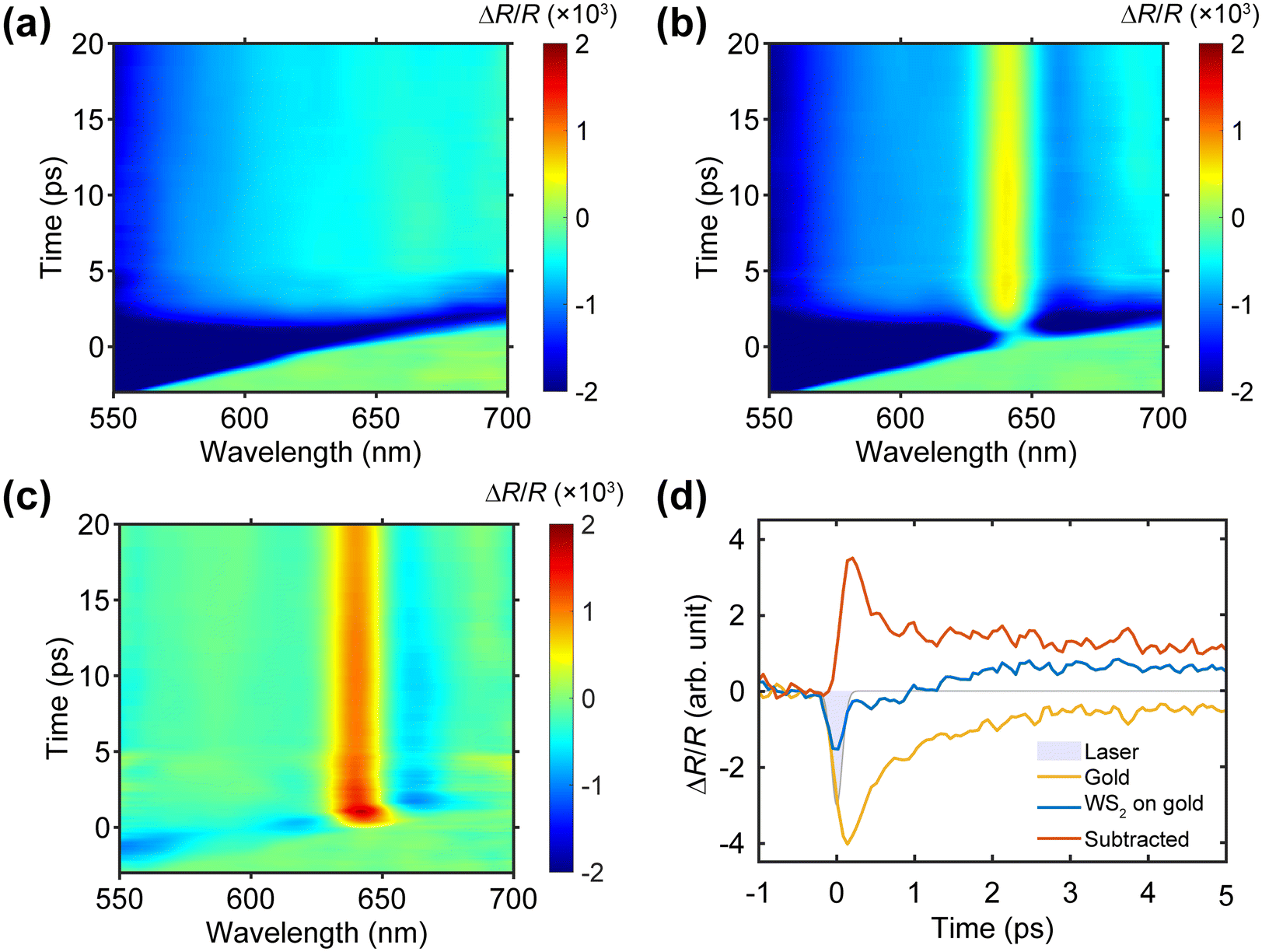 | ||
| Fig. 2 (a) Transient ΔR/R spectral map of the bare gold substrate obtained with pump excitation at 1100 nm. (b) Transient ΔR/R spectral map for the 1L-WS2/Au sample with a pump wavelength of 1100 nm. (c) ‘Background-corrected’ transient ΔR/R spectral map for the 1L-WS2/Au sample obtained by subtraction of the gold substrate response. (d) Kinetics of ΔR/R extracted at the positive peak of WS2 for bare gold substrate (yellow line) and 1L-WS2/Au (blue line), yielding the ‘background-corrected’ kinetics (orange line). The instrument response is shown by the gray area. | ||
To isolate the true transient response originating from 1L-WS2, we subtracted the ΔR/R response (Fig. 2a) of the bare gold film from that of 1L-WS2/Au (Fig. 2b). The resultant ΔR/R spectral map, shown in Fig. 2c, distills the distinct feature arising from the monolayer WS2 alone. We extracted the temporal kinetics of ΔR/R using the data in Fig. 2c at the wavelength of 640 nm and present the results in Fig. 2d. Interestingly, our analysis shows that the ‘background-corrected’ ΔR/R kinetics of 1L-WS2 exhibits a biexponential decay, resembling the response with above-bandgap pump excitation (see Fig. 1b). Similar transient reflectance spectra were also obtained for both 5L-WS2/Au and 10L-WS2/Au samples as illustrated in Fig. S3.† All three samples with different thicknesses of WS2 feature a band renormalization effect at the first 1 ps that can be attributed to a high concentration of excess free electrons present. As such, the TR response under 1100 nm pump excitation can be ascribed to pump-induced charge carrier injection into WS2.28,36–38 To explore this further, we conducted pump fluence-dependent measurements on both the 1L-WS2/gold sample and a sample with few-layer WS2 on gold. As summarized in Fig. S4,† we observed a linear relationship between the peak value of ΔR/R and the pump fluence. This linear relationship rules out the possibility of multi-photon absorption of the 1100-nm pump photons by WS2, thereby confirming the charge injection-induced ΔR/R response from gold to WS2 with 1100-nm, below-bandgap pump excitation.
In a low-perturbative regime, the alteration in reflectance of a semiconductor near its bandgap can be approximated as  , where ΔT denotes the temperature rise, Eg is the bandgap, and ΔN represents the change in the charge-carrier concentration of the semiconductor.39 Following the pump excitation, the initial response of ΔR/R is dominated by the dynamics of charge carrier, succeeded by the slower decay of lattice temperature. In the case of the 1L-WS2/Au sample, the lattice heating in both gold and WS2 is evident in the long-lived ΔR/R signal, persisting for hundreds of picoseconds (ps) after pump excitation, as illustrated in Fig. S5.† This extended feature of ΔR/R, emerging relatively late and peaking around 1000 ps, arises from a redshift of the exciton resonance of WS2 with an increasing temperature.40 This temperature rise in WS2 is induced by heat transfer from the nearby photothermally excited gold, as well as relaxation of hot carriers injected from gold.
In the initial time window (i.e., the first 20 ps after pump excitation), the ‘background-corrected’ signal of ΔR/R is primarily influenced by the change in charge carrier concentration in WS2. Consequently, the rapid rise of ΔR/R following pump excitation is associated with a growing concentration of injected electrons in the WS2. A similar response of ΔR/R was observed for three selected samples (i.e., 1L, 5L and 10L-thick WS2 on gold). We then extracted ‘background-corrected’ ΔR/R kinetics at the resonance reflectance dips for the three samples, namely 630 nm, 635 nm, and 640 nm, as illustrated in Fig. 1a. Informed by earlier studies, which demonstrated that the charge transfer between WS2 and graphene occurs within the first 20 fs,41 we anticipate that the charge injection dynamics cannot be resolved by our TR experiments. Nevertheless, as summarized in Fig. 3, the ΔR/R kinetics display a rapid rise upon pump excitation, followed by a bi-exponential decay comprising both fast and slow components with distinct time constants.
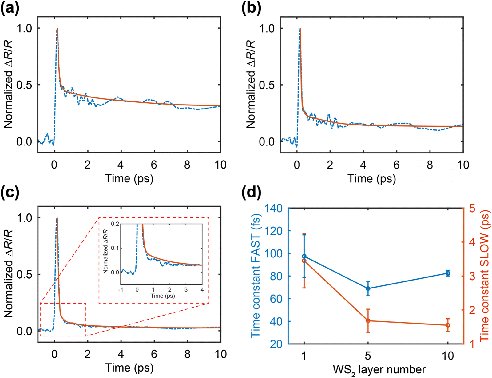 | ||
| Fig. 3 Normalized ΔR/R kinetics and its bi-exponential fitting for (a) 1L-WS2/Au, (b) 5L-WS2/Au, and (c) 10L-WS2/Au extracted at the corresponding A exciton wavelengths. The inset in (c) shows the zoom-in view of the ΔR/R signals after the initial 1 ps. (d) The fitted exponential time constants for the fast (left axis) and slow (right) components of the dynamics for the three samples. | ||
We fitted the ΔR/R kinetics using a bi-exponential function,  , where τf and τs represent the time constants for the fast and slow components, as summarized in Fig. 3d. The fast decay time constant τf, ranging from 70 to 100 fs, can be attributed to the cooling of injected hot electrons from a non-thermalized to a thermalized distribution. This timescale of τf aligns with prior literature reports on hot carrier thermalization in few-layer TMDs.42,43 Briefly, when the pump photon energy exceeds the SBH (denoted as ϕB), the injected electrons initially possess a non-thermal Gaussian distribution determined by the difference between pump photon energy and ϕB. The hot electrons undergo carrier-carrier scattering and rapidly reach a Fermi–Dirac distribution in the low-dimensional WS2 with reduced dielectric screening.
After relaxing to the conduction band edge, the thermalized electrons in WS2 traverse the WS2/Au interface, eventually decaying back to the gold substrate. This process is captured by the slow time constant, τs, which ranges from 1.5 to 3.4 ps and decreases with an increasing layer number of WS2. Similar processes have been observed in WS2/graphene heterostructures, where a carrier back-flow from WS2 to graphene takes approximately 1 ps.36,37,44–46 It is worth noting that the interlayer charge transfer time τs is, unlike τf, influenced by the interface of WS2 and gold rather than WS2 alone. The faster charge transfer observed in thicker WS2 can be attributed to improved contact between WS2 and gold, as well as a lower Schottky barrier, as discussed later. A more prolonged ΔR/R signal, persisting for hundreds to thousands of ps, follows the initial two exponential decay components; we attribute this long-lived ΔR/R component to the slow decay in lattice temperature in WS2 due to hot carrier relaxation, and potentially the extended trapping of electrons at the surface states.37 In the subsequent discussion, our focus is solely on the first 20 ps, which provides insights into the charge injection process of interest. We note that at this early time range, the significant heating effect in WS2 caused by the heat transfer from gold can be neglected.
As discussed earlier, the SBH at the WS2/Au interface is approximately 0.8 eV. This determination is drawn from literature reports on a threshold behavior in the current–voltage curves. Specifically, substantial drain–source currents were only detected when the bias voltage between the TMD and gold exceeded the Schottky barrier.15,18,24,25,47 Here, we hypothesize that the efficiency of pump-induced gold-to-WS2 charge injection varies with the pump photon energy. By sweeping the pump photon energy from above to below the SBH, we expect the charge injection efficiency to decrease substantially, thereby permitting the determination of the SBH.
We then performed TR experiments on the three WS2/Au samples (i.e., 1L, 5L and 10L-thick WS2 on gold) with systematically varied pump wavelengths under a fixed pump fluence. The ‘background-corrected’ ΔR/R kinetics are summarized in Fig. 4. Notably, the 1100-nm pump excitation induces ΔR/R signals in all three samples, and the magnitude of ΔR/R decreases with increasing pump wavelength. Importantly, we observed different threshold behaviors for the three samples. In the case of 1L-WS2/Au, the charge-transfer-induced ΔR/R signal is barely recognizable under 1200 nm pump wavelength (Fig. 4a). However, for 5L-WS2/Au, we observe ΔR/R even at 2000-nm pump excitation (Fig. 4b). For 10L-WS2/Au, a pump wavelength of 2400 nm still results in a discernable ΔR/R signal associated with charge carrier injection. Since the absolute magnitude of the ΔR/R signal at the initial time (<0.5 ps) is proportional to the concentration of injected electrons, these results imply that the three WS2 sample of different thicknesses possess different SBHs, with thicker (thinner) WS2 forming a lower (higher) Schottky barrier with gold.
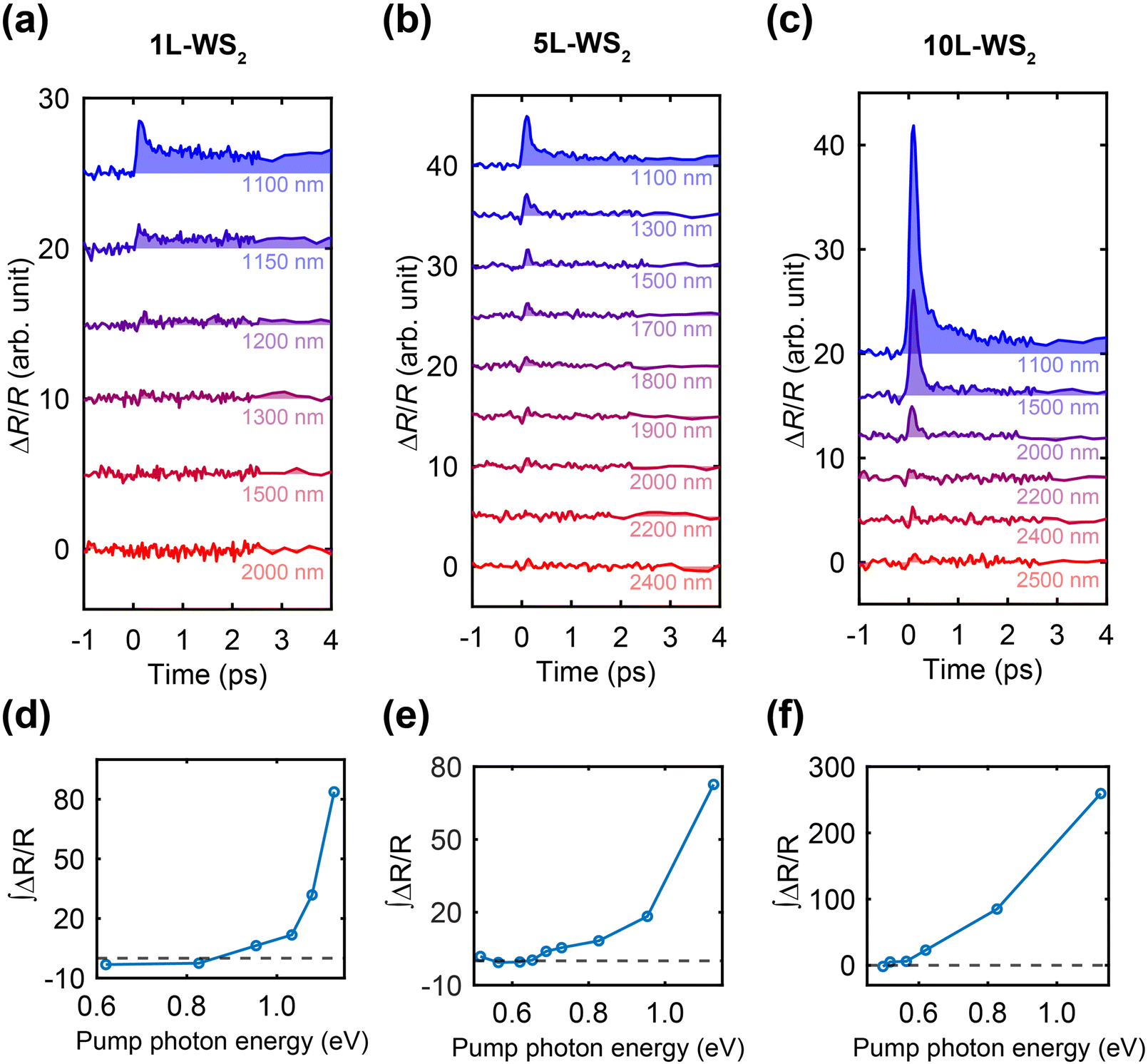 | ||
| Fig. 4 The pump-wavelength dependent kinetics of (a) 1L-WS2/Au, (b) 5L-WS2/Au, and (c) 10L-WS2/Au, extracted at the corresponding A exciton wavelengths. The kinetics are offset for clarify of presentation. The ΔR/R kinetics are integrated over the first 4 ps for (d) 1L-WS2/Au, (e) 5L-WS2/Au, and (f) 10L-WS2/Au, with pump wavelength converted to pump photon energy in eV. | ||
To extract the SBH, we plotted the trend of integrated ΔR/R with the pump photon energy in Fig. 4d–f for the three samples. In these plots, we integrated ΔR/R over a short, early time window (i.e., the first 4 ps) to exclude effects due to interface-trapped electrons and material heating. As expected, a threshold behavior in the pump photon energy is observed for all three samples, and no ΔR/R signal and the associated charge injection are observed below the respective threshold pump photon energy for each sample. Based on the cut-off pump photon energy, we can extract the SBHs for the three samples with 1L, 5L and 10L WS2 to be approximately 0.85 eV, 0.65 eV and 0.50 eV. Note that the measurements for each sample under a certain pump photon energy are repeated three times and then averaged out. The standard errors of the integrated kinetics (see Fig. S6†) indicate a good reproducibility.
In addition to the decreasing trend of SBH with the thickness of WS2, a distinct kink is evident in Fig. 4d and f for 1L-WS2 and 5L-WS2, respectively. In these cases, the rise in integrated ΔR/R with pump photon energy displays two different slopes. Notably, such a trend is not observed in the thicker, 10L-WS2. We attribute this observation to the evolution of the WS2 band structure with increasing layer number, as the SBH at the WS2/Au interface correlates with the conduction band of WS2. Considering a simple Schottky barrier formed at this interface, neglecting surface states and Fermi level pinning, the SBH of the junction, ϕB, depends solely on the difference between the work function of gold (Wau) and the electron affinity of WS2 (χe), given by ϕB = Wau − χe.15,48 WS2 undergoes a crossover from an indirect to a direct bandgap as the thickness increases from a monolayer to multilayer. Consequently, the bandgap experiences a redshift with an increasing layer number due to the lowering of the local conduction band minimum (CBM) at the midpoint between the Γ and the K points of the Brillouin zone, namely the Q valley.15,34,49 This shift of CBM with layer number is responsible for the observed decrease in ϕB from TR experiments on thicker WS2 interfaced with gold. We note that similar trend of SBH with the number of TMD layer has been reported on the MoS2/Au interface, where the ϕB decreases from 0.8 eV to 0.2 eV when the layer number goes from one to five.15
We hypothesize that the observed kinks in the 1L-WS2/Au and 5L-WS2/Au samples (Fig. 4d and e), contrasted with their absence in the 10L-WS2/Au sample (Fig. 4f), stem from variations in the density of states (DOS) near the CBM of WS2. Specifically, we anticipate that the injection probability of pump-excited hot electrons from gold to WS2, surmounting the Schottky barrier, should exhibit a linear dependence on the available states in WS2. To test this hypothesis, we performed density functional theory (DFT) calculations of the band structures and DOS of 1L- and 5L-WS2, as presented in Fig. 5a and b, respectively. In the DFT results, the CBM was chosen as the zero-energy point, hence the vertical axis indicates the excess energy of injected hot electrons. The maximal excess energy of injected hot electrons is equal to the pump photon energy minus the SBH.
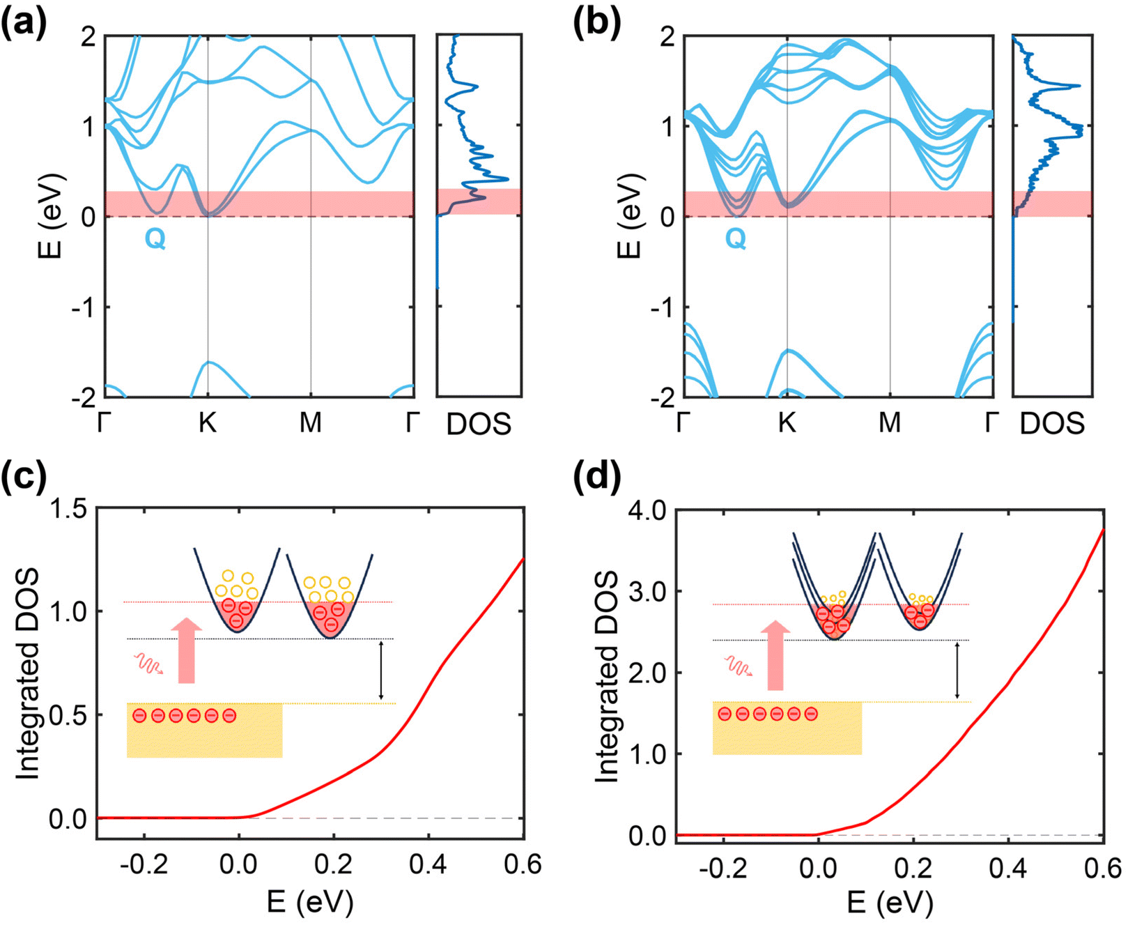 | ||
| Fig. 5 Calculated DFT band structures and conduction-band density of states (DOS) of (a) 1L-WS2 and (b) 5L-WS2. The conduction band minimum at each diagram is set as the zero-energy point. The shadow indicates the available states for injected electrons with energy larger than the Schottky barrier. The DOS integrated over the shadowed energy window are shown in (c) for 1L-WS2 and (d) for 5L-WS2. | ||
Assuming equal probability of injection for hot electrons into any lower-lying energy states, we integrated the DOS with respect to energy below the maximum excess energy level. This integration yields the total number of states available for electron injection. The energy cutoff in the integration corresponds directly to the pump photon energy. The results of this integration are shown in Fig. 5c for 1L-WS2 and in Fig. 5d for 5L-WS2. Notably, and in line with the TR experiments, a distinctive kink is evident in the plot of integrated DOS versus energy for 1L-WS2, stemming from the peak in the DOS corresponding to an M0-type van Hove singularity occurring at the six-fold degenerate valley along the Λ high-symmetry path from Gamma to K (sometimes referred to as the Q valley). In contrast, such a kink is absent in the plot for 5L-WS2, attributable to its smoothly varying DOS with energy. Qualitatively, this disparity between 1L-WS2 and 5L-WS2 arises from the near continuum of conduction bands in the latter, providing a greater, and more smoothly varying pool of available DOS for hosting the injected electrons.
Conclusion
In summary, we have introduced and validated an all-optical method for probing the SBH at interfaces between 2D-TMDs and metals, utilizing the WS2/Au interface as a representative model system. Through nuanced comparison of transient reflection results obtained from WS2/Au and a bare gold substrate, we identified the spectral and temporal signatures associated with interfacial charge transfer. By systematically varying the pump wavelength across the near- to mid-infrared range, traversing the SBH, we quantified the SBHs for WS2/Au samples with varying WS2 thicknesses from monolayer to 10 layers, and discussed how the charge injection efficiency correlates with the DOS in WS2. Importantly, this non-contact approach is versatile and can be generalized for investigating the energy alignment of diverse 2D-TMD/metal interfaces, providing insights into their interfacial quality, and advancing the understanding and control of 2D materials in the context of nanoelectronic and nanophotonic applications.Author contributions
P. G. and D. J. conceived the project. P. G. supervised the project. D. C. performed optical measurements. S. B. A. and D. J. fabricated the samples. J. W. and D. Y. Q. performed DFT calculations. D. C. wrote the manuscript with inputs from co-authors.Conflicts of interest
There are no conflicts of interest to declare.Acknowledgements
This material is based upon work supported by the National Science Foundation under Grant No. CBET-2315077. P. G. acknowledges the partial support from the Air Force Office of Scientific Research under Grant No. FA9550-22-1-0209. D. J. and S. B. acknowledge partial support from Asian Office of Aerospace Research and Development of the Air Force Office of Scientific Research (AFOSR) (FA2386-21-1-4063) and the Office of Naval Research (N00014-23-1-203). Theoretical calculations by J. W. and D. Y. Q. were supported by the National Science Foundation (NSF) Condensed Matter and Materials Theory (CMMT) program under Grant DMR-2114081.References
- B. Radisavljevic, A. Radenovic, J. Brivio, V. Giacometti and A. Kis, Nat. Nanotechnol., 2011, 6, 147–150 CrossRef CAS PubMed.
- J. Y. Lim, M. Kim, Y. Jeong, K. R. Ko, S. Yu, H. G. Shin, J. Y. Moon, Y. J. Choi, Y. Yi, T. Kim and S. Im, npj 2D Mater. Appl., 2018, 2, 37 CrossRef.
- D. Xiao, G.-B. Liu, W. Feng, X. Xu and W. Yao, Phys. Rev. Lett., 2012, 108, 196802 CrossRef PubMed.
- T. Cao, G. Wang, W. Han, H. Ye, C. Zhu, J. Shi, Q. Niu, P. Tan, E. Wang, B. Liu and J. Feng, Nat. Commun., 2012, 3, 887 CrossRef PubMed.
- B. W. H. Baugher, H. O. H. Churchill, Y. Yang and P. Jarillo-Herrero, Nat. Nanotechnol., 2014, 9, 262–267 CrossRef CAS PubMed.
- O. Lopez-Sanchez, D. Lembke, M. Kayci, A. Radenovic and A. Kis, Nat. Nanotechnol., 2013, 8, 497–501 CrossRef CAS PubMed.
- N. Perea-López, A. L. Elías, A. Berkdemir, A. Castro-Beltran, H. R. Gutiérrez, S. Feng, R. Lv, T. Hayashi, F. López-Urías, S. Ghosh, B. Muchharla, S. Talapatra, H. Terrones and M. Terrones, Adv. Funct. Mater., 2013, 23, 5511–5517 CrossRef.
- M. M. Furchi, A. Pospischil, F. Libisch, J. Burgdörfer and T. Mueller, Nano Lett., 2014, 14, 4785–4791 CrossRef CAS PubMed.
- C.-H. Lee, G.-H. Lee, A. M. van der Zande, W. Chen, Y. Li, M. Han, X. Cui, G. Arefe, C. Nuckolls, T. F. Heinz, J. Guo, J. Hone and P. Kim, Nat. Nanotechnol., 2014, 9, 676–681 CrossRef CAS PubMed.
- A. Pospischil, M. M. Furchi and T. Mueller, Nat. Nanotechnol., 2014, 9, 257–261 CrossRef CAS PubMed.
- S. Jo, N. Ubrig, H. Berger, A. B. Kuzmenko and A. F. Morpurgo, Nano Lett., 2014, 14, 2019–2025 CrossRef CAS PubMed.
- O. Lopez-Sanchez, E. A. Llado, V. Koman, A. Fontcuberta i Morral, A. Radenovic and A. Kis, ACS Nano, 2014, 8, 3042–3048 CrossRef CAS PubMed.
- F. Withers, O. Del Pozo-Zamudio, A. Mishchenko, A. P. Rooney, A. Gholinia, K. Watanabe, T. Taniguchi, S. J. Haigh, A. K. Geim, A. I. Tartakovskii and K. S. Novoselov, Nat. Mater., 2015, 14, 301–306 CrossRef CAS PubMed.
- E. Pollmann, S. Sleziona, T. Foller, U. Hagemann, C. Gorynski, O. Petri, L. Madauß, L. Breuer and M. Schleberger, ACS Omega, 2021, 6, 15929–15939 CrossRef CAS PubMed.
- H. Lee, S. Deshmukh, J. Wen, V. Z. Costa, J. S. Schuder, M. Sanchez, A. S. Ichimura, E. Pop, B. Wang and A. K. M. Newaz, ACS Appl. Mater. Interfaces, 2019, 11, 31543–31550 CrossRef CAS PubMed.
- P.-C. Shen, C. Su, Y. Lin, A.-S. Chou, C.-C. Cheng, J.-H. Park, M.-H. Chiu, A.-Y. Lu, H.-L. Tang, M. M. Tavakoli, G. Pitner, X. Ji, Z. Cai, N. Mao, J. Wang, V. Tung, J. Li, J. Bokor, A. Zettl, C.-I. Wu, T. Palacios, L.-J. Li and J. Kong, Nature, 2021, 593, 211–217 CrossRef CAS PubMed.
- J. R. Lince, D. J. Carré and P. D. Fleischauer, Phys. Rev. B: Condens. Matter Mater. Phys., 1987, 36, 1647–1656 CrossRef CAS PubMed.
- C. Kim, I. Moon, D. Lee, M. S. Choi, F. Ahmed, S. Nam, Y. Cho, H.-J. Shin, S. Park and W. J. Yoo, ACS Nano, 2017, 11, 1588–1596 CrossRef CAS PubMed.
- J. Su, N. Li, Y. Zhang, L. Feng and Z. Liu, AIP Adv., 2015, 5, 077182 CrossRef.
- Y. Guo, D. Liu and J. Robertson, ACS Appl. Mater. Interfaces, 2015, 7, 25709–25715 CrossRef CAS PubMed.
- Y. Liu, P. Stradins and S.-H. Wei, Sci. Adv., 2016, 2, e1600069 CrossRef PubMed.
- I. Popov, G. Seifert and D. Tománek, Phys. Rev. Lett., 2012, 108, 156802 CrossRef PubMed.
- S. Das, H.-Y. Chen, A. V. Penumatcha and J. Appenzeller, Nano Lett., 2013, 13, 100–105 CrossRef CAS PubMed.
- N. Kaushik, A. Nipane, F. Basheer, S. Dubey, S. Grover, M. M. Deshmukh and S. Lodha, Appl. Phys. Lett., 2014, 105, 113505 CrossRef.
- H. Qiu, L. Pan, Z. Yao, J. Li, Y. Shi and X. Wang, Appl. Phys. Lett., 2012, 100, 123104 CrossRef.
- K. Jo, P. Kumar, J. Orr, S. B. Anantharaman, J. Miao, M. J. Motala, A. Bandyopadhyay, K. Kisslinger, C. Muratore, V. B. Shenoy, E. A. Stach, N. R. Glavin and D. Jariwala, ACS Nano, 2021, 15, 5618–5630 CrossRef CAS PubMed.
- M. Fontana, T. Deppe, A. K. Boyd, M. Rinzan, A. Y. Liu, M. Paranjape and P. Barbara, Sci. Rep., 2013, 3, 1634 CrossRef PubMed.
- K. R. Keller, R. Rojas-Aedo, H. Zhang, P. Schweizer, J. Allerbeck, D. Brida, D. Jariwala and N. Maccaferri, ACS Photonics, 2022, 9, 2683–2690 CrossRef CAS PubMed.
- W. M. H. Sachtler, G. J. H. Dorgelo and A. A. Holscher, Surf. Sci., 1966, 5, 221–229 CrossRef CAS.
- S. H. Lee, D. Lee, W. S. Hwang, E. Hwang, D. Jena and W. J. Yoo, Appl. Phys. Lett., 2014, 104, 193113 CrossRef.
- Z. Li, G. Ezhilarasu, I. Chatzakis, R. Dhall, C.-C. Chen and S. B. Cronin, Nano Lett., 2015, 15, 3977–3982 CrossRef CAS PubMed.
- S. Schmitt-Rink, D. S. Chemla and D. A. B. Miller, Phys. Rev. B: Condens. Matter Mater. Phys., 1985, 32, 6601–6609 CrossRef CAS PubMed.
- M. Okada, N. Okada, W.-H. Chang, T. Endo, A. Ando, T. Shimizu, T. Kubo, Y. Miyata and T. Irisawa, Sci. Rep., 2019, 9, 17678 CrossRef PubMed.
- W. Zhao, Z. Ghorannevis, L. Chu, M. Toh, C. Kloc, P.-H. Tan and G. Eda, ACS Nano, 2013, 7, 791–797 CrossRef CAS PubMed.
- F. Ceballos and H. Zhao, Adv. Funct. Mater., 2017, 27, 1604509 CrossRef.
- C. Trovatello, G. Piccinini, S. Forti, F. Fabbri, A. Rossi, S. De Silvestri, C. Coletti, G. Cerullo and S. Dal Conte, npj 2D Mater. Appl., 2022, 6, 24 CrossRef CAS.
- S. Fu, I. du Fossé, X. Jia, J. Xu, X. Yu, H. Zhang, W. Zheng, S. Krasel, Z. Chen, Z. M. Wang, K.-J. Tielrooij, M. Bonn, A. J. Houtepen and H. I. Wang, Sci. Adv., 2021, 7, eabd9061 CrossRef CAS PubMed.
- A. Chernikov, C. Ruppert, H. M. Hill, A. F. Rigosi and T. F. Heinz, Nat. Photonics, 2015, 9, 466–470 CrossRef CAS.
- P. Guo, A. Mannodi-Kanakkithodi, J. Gong, Y. Xia, C. C. Stoumpos, D. H. Cao, B. T. Diroll, J. B. Ketterson, G. P. Wiederrecht, T. Xu, M. K. Y. Chan, M. G. Kanatzidis and R. D. Schaller, Nat. Commun., 2019, 10, 482 CrossRef PubMed.
- D. Chen, M. Fortin-Deschênes, Y. Lou, H. Lee, J. Xu, A. A. Sheikh, K. Watanabe, T. Taniguchi, Y. Xia, F. Xia and P. Guo, J. Phys. Chem. C, 2023, 127, 9121–9128 CrossRef CAS.
- M. Massicotte, P. Schmidt, F. Vialla, K. Watanabe, T. Taniguchi, K. J. Tielrooij and F. H. L. Koppens, Nat. Commun., 2016, 7, 12174 CrossRef CAS PubMed.
- Z. Nie, R. Long, L. Sun, C.-C. Huang, J. Zhang, Q. Xiong, D. W. Hewak, Z. Shen, O. V. Prezhdo and Z.-H. Loh, ACS Nano, 2014, 8, 10931–10940 CrossRef CAS PubMed.
- T. Wang, T. R. Hopper, N. Mondal, S. Liu, C. Yao, X. Zheng, F. Torrisi and A. A. Bakulin, ACS Nano, 2023, 17, 6330–6340 CrossRef CAS PubMed.
- S. Aeschlimann, A. Rossi, M. Chávez-Cervantes, R. Krause, B. Arnoldi, B. Stadtmüller, M. Aeschlimann, S. Forti, F. Fabbri, C. Coletti and I. Gierz, Sci. Adv., 2020, 6, eaay0761 CrossRef CAS PubMed.
- Y. Chen, Y. Li, Y. Zhao, H. Zhou and H. Zhu, Sci. Adv., 2019, 5, eaax9958 CrossRef CAS PubMed.
- L. Yuan, T.-F. Chung, A. Kuc, Y. Wan, Y. Xu, Y. P. Chen, T. Heine and L. Huang, Sci. Adv., 2018, 4, e1700324 CrossRef PubMed.
- W. Zhai, J. Qi, C. Xu, B. Chen, Z. Li, Y. Wang, L. Zhai, Y. Yao, S. Li, Q. Zhang, Y. Ge, B. Chi, Y. Ren, Z. Huang, Z. Lai, L. Gu, Y. Zhu, Q. He and H. Zhang, J. Am. Chem. Soc., 2023, 145, 13444–13451 CrossRef CAS PubMed.
- A. M. Cowley and S. M. Sze, J. Appl. Phys., 2004, 36, 3212–3220 CrossRef.
- J. Kang, S. Tongay, J. Zhou, J. Li and J. Wu, Appl. Phys. Lett., 2013, 102, 012111 CrossRef.
Footnote |
| † Electronic supplementary information (ESI) available. See DOI: https://doi.org/10.1039/d3nr05799b |
| This journal is © The Royal Society of Chemistry 2024 |