
 Open Access Article
 This Open Access Article is licensed under a Creative Commons Attribution-Non Commercial 3.0 Unported Licence
Quantifying the effect of nanosheet dimensions on the piezoresistive response of printed graphene nanosheet networks†
Eoin
Caffrey
 a,
Jose M.
Munuera
ab,
Tian
Carey
a and
Jonathan N.
Coleman
*a
a,
Jose M.
Munuera
ab,
Tian
Carey
a and
Jonathan N.
Coleman
*a
aSchool of Physics, CRANN & AMBER Research Centres, Trinity College Dublin, Dublin 2, Ireland. E-mail: colemaj@tcd.ie; Tel: +353 (0) 1 8963859
bPhysics Department, University of Oviedo, C/Federico García Lorca no 18, 33007 Oviedo, Spain
First published on 31st July 2024
Abstract
Printed networks of 2D nanosheets have found a range of applications in areas including electronic devices, energy storage systems and sensors. For example, the ability to print graphene networks onto flexible substrates enables the production of high-performance strain sensors. The network resistivity is known to be sensitive to the nanosheet dimensions which implies the piezoresistance might also be size-dependent. In this study, the effect of nanosheet thickness on the piezoresistive response of nanosheet networks has been investigated. To achieve this, we liquid-exfoliated graphene nanosheets which were then subjected to centrifugation-based size selection followed by spray deposition onto flexible substrates. The resultant devices show increasing resistivity and gauge factor with increasing nanosheet thickness. We analyse the resistivity versus thickness data using a recently reported model and develop a new model to fit the gauge factor versus thickness data. This analysis allowed us to differentiate between the effect of strain on inter-nanosheet junctions and the straining of the individual nanosheets within the network. Surprisingly, our data implies the nanosheets themselves to display a negative piezo response.
New conceptsWhile many papers have reported experimental data on the piezoresistance of graphene-based films and composites, much less has been done to understand the piezoresistive mechanism. We have very recently reported models explaining how the resistivity of printed graphene networks depends on the nanosheet dimensions as well as experiments supporting those models. These new insights imply that the network piezoresistance should also be nanosheet size-dependent. Here we demonstrate this to be the case and derive a model to explain the data. Surprisingly, fitting the data to the model implies the nanosheets to have negative piezoresistance, which is unexpected. This approach is novel because most papers on piezo resistance of nano networks report the results of measurements without any theoretical framework to aid understanding. Here, combining experiments with a model gives added insights into the piezo resistive mechanism. Moreover, it provides the unexpected result that the nanosheets themselves have negative piezo resistance. |
Introduction
In recent years, 2D materials have been much studied because of their combination of exciting physical properties and applications potential.1–4 Liquid phase exfoliation (LPE) provides a scalable, cost-effective technique to convert layered materials to few layer nanosheets in large quantities.5,6 This technique was applied first to graphene,5 but subsequently to a whole host of layered materials including h-BN,7 TMDs,8 BP9 and even layered silicates.10 LPE produces nanosheets of relatively low aspect ratios (∼10–100)11 which are suspended in liquid media. These inks are ideal for subsequent processing. For example, a technique known as liquid cascade centrifugation can be used to size select the nanosheets either for characterisation or for subsequent applications.12–14 Alternatively, these nanosheet inks can be mixed with polymers or other nanomaterials to form nanocomposites.15–17 The nanosheets can be deposited onto substrates using techniques such as inkjet printing,18,19 aerosol jet printing20 and spray coating.21 Printing yields thin films of nanosheets, often referred to as networks.The properties of nanosheet networks are strongly influenced by their morphologies.22,23 For example, low aspect ratio nanosheets produced by LPE tend to form disordered, poorly aligned, highly porous networks. These networks are characterised by inter nanosheet junctions which hinder charge transport.24 To cross a junction, charge carriers must overcome a potential barrier, resulting in the presence of a junction resistance. The magnitude of the junction resistance is determined by the network morphology and effectively controls the mobility and so conductivity of charge carriers within the network. Printed nanosheet networks have been used to fabricate a range of electronic devices including transistors,25 solar cells26 and diodes.27 The junction resistance is an important factor which limits the performance of these devices.
One important property of nanosheet networks is piezoresistivity.21,28–30 This effect describes the change in resistance of a material in response to mechanical deformation. It is now well known that applying strain in the plane of a nanosheet network results in a measurable change in the electrical resistance of the network.21 Similar behaviour is seen in a range of networks, including those consisting of nanosheets or nanotubes embedded in polymer matrices (i.e. nanocomposites).16,31–33 This resistance change is almost always attributed to the effect of strain on the junction resistance,34–37 although network morphology effects23 as well as geometrical Poisson effects have been discussed.35
The magnitude of the piezoresistive effect can be quantified using a metric known as the gauge factor (G), which is defined as the fractional change in resistance from the unstrained position, per unit strain:38
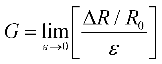 | (1) |
Clearly, large values of G are associated with a large piezoresistive effect. In practical terms, the gauge factor is an important material parameter such that materials with high values of G could be used to fabricate sensitive strain sensors.30,39 The piezoresistive phenomenon in nanosheet networks, particularly conductive networks of graphene nanosheets, has previously been exploited to fabricate piezoresisitve films and nanocomposite materials for applications in strain sensing.21,40–46 Conversely, material with very small G could find application in flexible electronic devices47 or strain invariant electrical interconnects.48 Developing and controlling this effect will be critical if the vision of high sensitivity sensors or flexible electronics technology based on networks of 2D nanosheets is to be realised.
Much research has been conducted to optimise and maximise the gauge factor in various network materials.17,30,43,49 One fruitful approach has been to combine theoretical modelling with experimental data to understand the factors controlling G in piezoresistive nanosheet networks. It has become clear that there is a well-defined link between network conductivity or resistivity and the gauge factor of the network. Recent studies have modulated the network conductivity either by controlling the nanosheet content in polymer–graphene nanocomposites,50 by controlling the composition of mixtures of conducting and semiconducting nanosheets40 or by controlling the thickness of very thin nanosheet networks.23 In each case, the link between G and conductivity has been established experimentally and understood theoretically. These studies have cast significant light on both conductive and piezoresistive processes in these systems.
However, there is one very obvious parameter that should affect the piezoresistance in nanosheet networks that has not been explored: nanosheet size and thickness. FIB–SEM nanotomography has shown that network morphology varies with nanosheet size.22 In addition, various papers have shown that varying the nanosheet dimensions have a substantial impact on network resitivity.22,51,52 Significantly, a very recent paper has reported a simple model which quantifies the relationship between network resistivity and nanosheet dimensions as well as the effect of parameters associated with network morphology such as junction resistance, porosity and tortuosity.53
Here we study the effect of nanosheet dimensions, specifically thickness, on the piezoresistive properties of printed graphene nanosheet networks. By focusing on networks with thickness of a micron or more, we can ensure that they display bulklike resistivity without any percolative effects.23 In this way the piezoresistive response will be free from effects associated with the effect of strain on the structure of the network. By combining experiments with simple theoretical models, we will show that the network piezoresistivity is limited by the effect of strain on both the inter-nanosheet junctions and the resistivity of the nanosheets themselves.
Results and discussion
Material characterisation
Dispersions of graphene nanosheets were produced by liquid phase exfoliation (LPE)5,54,55 of graphite powder in n-methyl-2-pyrollidone (NMP). The resultant dispersions were then size selected into various fractions using liquid cascade centrifugation,14 a process based on repeated centrifugation and separation steps which is shown schematically in Fig. 1A. Shown in Fig. 1B is a photograph of the resulting size selected fractions after solvent exchange into isopropanol (IPA). An ink concentration of 0.1 mg mL−1 was chosen for spray coating. Although all inks looked to be identical black liquids, differences between them can be observed by measuring their extinction spectra in the UV-visible region as shown in Fig. 1C. Here, the characteristic π–π* transition peak at ∼267 nm observed as well as the long wavelength plateau.56 Notably, as the centrifugation speed used to sediment the nanosheets increases, and the nanosheets in the ink become smaller and thinner, the amplitude of the peak relative to the plateau value increases in line with observations by Backes et al.57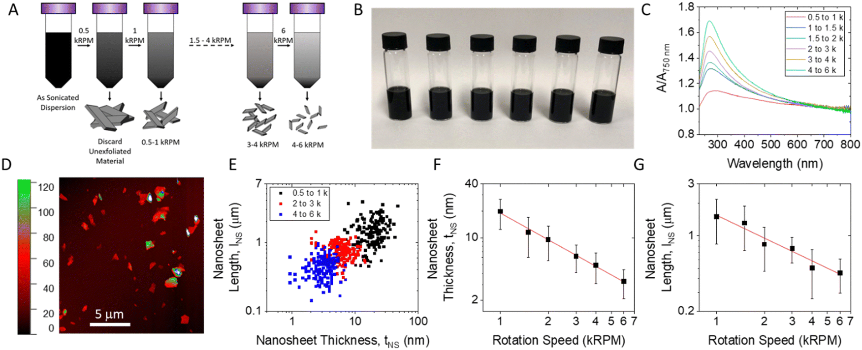 | ||
| Fig. 1 Size selected nanosheet inks. (A) Schematic illustrating the process of liquid cascade centrifugation, where the larger sheets are sedimented at lower centrifugation speeds. (B) Photograph of the size selected nanosheet inks. (C) Extinction spectra of the size selected nanosheets, normalised at 750 nm. (D) AFM image of nanosheets 1.5 to 2 kRPM fraction, scale bar 5 μm, height scale is in nm. (E) Plot of individual nanosheet length vs. nanosheet thickness measured by AFM for nanosheets from three different size-selected fractions. Such data was used to determine the mean nanosheet length and thickness for each fraction. (F) Plot of mean nanosheet thickness vs. rotation speed. (G) Plot of mean nanosheet length vs. rotation speed. The lines in F and G are power law fits with exponents close to −1. The errors in F and G are standard deviations and represent the spread of the distribution. | ||
To enable proper analysis, it is important to measure the lateral size and thickness of the nanosheets in each fraction. To this end, the nanosheet length and thickness distributions were quantified using atomic force microscopy (AFM) for all samples, with a representative AFM image shown in Fig. 1D. Other sample images are shown in the ESI.† When performing AFM of solution processed nanosheets, various studies have shown that for liquid exfoliated nanosheets, heights obtained directly from AFM measurements overestimate nanosheet thickness, probably due to a combination of tip/sample/substrate interaction effects and the presence of adsorbed solvent. Various papers have reported correction protocols to convert the apparent nanosheet thickness to the real thickness, as described in methods.6,14,58,59 Examples of apparent and real nanosheet thickness measurements (i.e. before and after correction) are shown in the ESI.† The nanosheet length (LNS) is plotted versus the corrected nanosheet thickness (tNS) on a flake-by-flake basis in Fig. 1E for three of the six fractions studied. The mean values of LNS and tNS are plotted versus the upper RPM associated with each step of the liquid cascade certification process (see Methods). These results verified that as the centrifugation speed increased the nanosheets selected into each fraction became smaller and thinner. As observed previously both nanosheet length and thickness decayed as a power law with RPM.11,14,24,57
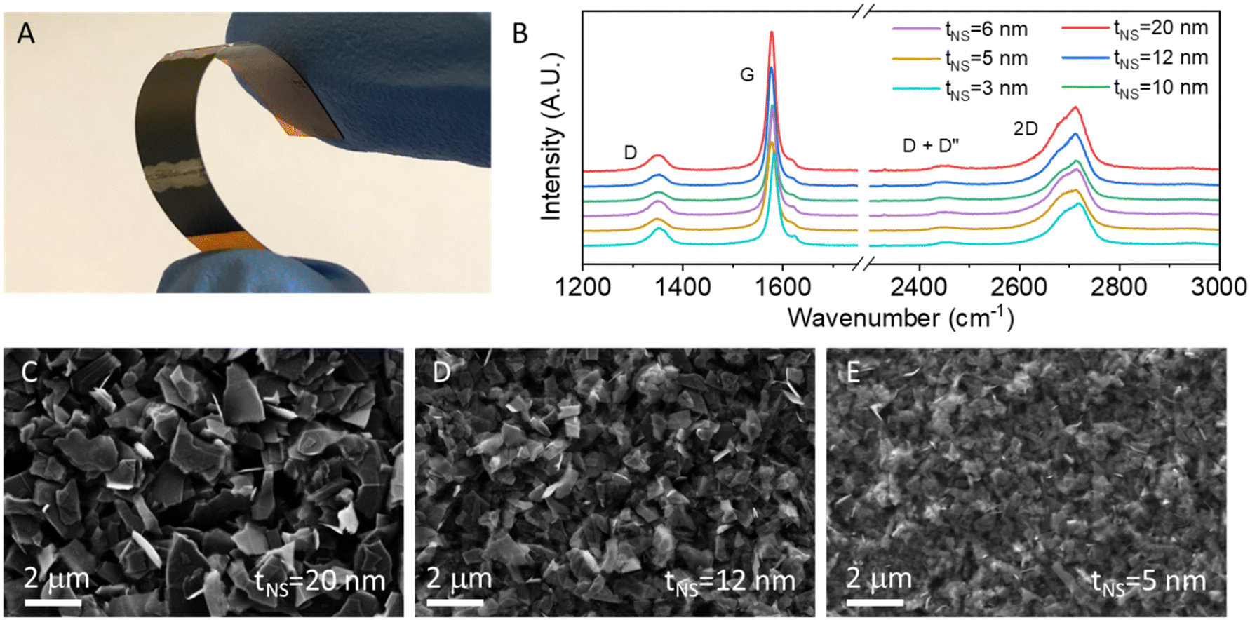 | ||
| Fig. 2 Network characterisation. (A) Image of a network sprayed on Kapton, bent between fingers. (B) Raman spectra measured on graphene films sprayed from each size selected ink. (C)–(E) Top-down SEM of the networks of (C) large (0.5 to 1 kRPM) and (D) medium (1.5 to 2 kRPM) and (E) small (3 to 4 kRPM) size selected nanosheets. In (C)–(E) the mean nanosheet thickness, tNS, is given in the panel. | ||
Inks such as these can be used to prepare thin films by a range of solution–deposition methods.1,24,60 Here, we produced films by spray coating onto flexible Kapton substrates (Fig. 2A), yielding grey opaque films with thickness in the range 1 to 3 μm, as measured by optical profilometry (methods). Such relatively thick films were produced to avoid percolation effects often found in thinner films and to achieve thickness-independent film resistivity.19,23,61–65 This means that the piezoresistive response will be free from effects associated with the influence of strain on the structure of the network.23 Raman spectra measured on these films (Fig. 2B) showed the characteristic D, G and 2D peaks as well as some evidence of the D + D′′ peak.66 These peaks are consistent with other reports for liquid phase exfoliated graphene materials.67 The D![[thin space (1/6-em)]](https://www.rsc.org/images/entities/char_2009.gif) :G intensity ratio decreases gradually with increasing nanosheet size, consistent with the effects of edge defects.57
:G intensity ratio decreases gradually with increasing nanosheet size, consistent with the effects of edge defects.57
SEM images of the top surfaces of the networks containing the largest and the smallest nanosheets are shown in Fig. 2C–E. These images show considerable disorder with relatively poor flake alignment and significant surface roughness seen in each of the films. This is consistent with spray coated LPE nanosheet networks, which yield jammed networks of nanosheets.22
Electrical resistivity of thick nanosheet networks
In order to measure the electrical properties of these films, electrodes were carefully painted using silver paste. This gave a set of channels with widths ranging from 4 to 6 mm and channel lengths in the range 0.8–1.0 cm. Each channel length and width were measured individually. We measured the thin film resistivity (at zero strain), finding values in the range 2–7 × 10⁻⁴ Ω m, depending on the dimensions of the nanosheets making up the film. The measured network resistivity, ρNet, is plotted versus mean nanosheet thickness, tNS, in Fig. 3A and shows a well-defined linear trend. Variations in network resistivity with nanosheet size have been observed previously, for example by Clifford et al.,68 with linear behaviour similar to that shown in Fig. 3A reported by Gabbett et al.53 | ||
| Fig. 3 (A) Plot of network resistivity vs. nanosheet thickness, showing a linear relationship. (B) Plot of fractional change in resistance vs. strain for films prepared from nanosheets of each size. The slope is shown to increase with increasing nanosheet size. Strained to 0.5% at a strain rate of 0.2% s−1. (C) Distributions of measured gauge factor for a device from each size range. From cycling experiment with a triangular sawtooth strain wave, 0.5% amplitude, 0.2% s−1 strain rate. (D) Plot of gauge factor as a function of nanosheet thickness, with a fit to the model given by eqn (5). The red dashed line represents the modified model as described in the text. | ||
We can quantitively analyse this data as follows. It is well known that networks of nanosheets with thickness above some critical value (referred to as tx) display bulklike conductivity while thinner networks display thickness-dependent conductivity due to percolation effects.19,23,61–65 For spray coated graphene nanosheets prepared by LPE the percolation to bulklike transition occurs at tx ∼ 100 nm (ref. 23) although it is likely to be much lower (tx ∼ 10 nm) for electrochemically exfoliated nanosheets.69 It has been shown that for networks of conductive 2D materials which are thick enough to display bulklike conduction, the network resistivity is given by53
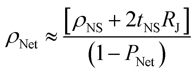 | (2) |
That the data in Fig. 3A is linear as predicted by eqn (2) implies that the junction resistance is independent of nanosheet thickness. Because nanosheet length scales with nanosheet thickness as shown in Fig. 1E–G, this also implies RJ to be independent of nanosheet length. This has important implications. If the nanosheets were well-aligned such that the inter-nanosheet junctions consisted of conformal, large-area overlaps between adjacent nanosheets, then we would expect junction area and hence RJ to scale with nanosheet length. That RJ is independent of nanosheet length implies we do not have such conformal junctions. Rather we propose the junctions in networks such as these spray cast films of LPE nanosheets are pointlike and so independent of nanosheet size. This hypothesis is consistent with recent nano-tomography data measured on similar nanosheet networks.22
It is worth noting that resistivity data in general is limited by accurate knowledge of film thickness. Systematic errors in film thickness would lead to errors in the slope and intercept associated with linear fitting to eqn (2). Specific to nano-networks, imperfect knowledge of the network porosity will lead to similar errors. The effects of tortuosity (although assumed to be unimportant in eqn (2), they can be accounted for in more detailed models: see SI of ref. 53) can also introduce such systematic errors. However, taking the ratio of slope to intercept for a ρNetversus tNS graph yields a value of 2RJ/ρNS which is free from such errors. Here, from the fit to Fig. 3A, we find 2RJ/ρNS = 6.13 × 10⁸ m−1.
Piezoresistive properties of thick nanosheet networks
We measured the piezoresistive properties of the set of films with varying nanosheet dimensions (Fig. 1) using a tensile tester specially modified to measure resistance as a function of applied strain (and stress). The gauge factor of the network, GNet, can then be calculated using eqn (1). As the gauge factor is strictly defined as the linear response in the limit of low strain, it was imperative to work at low strain. Preliminary results showed the resistance versus strain curves to be linear up to 1% strain. Subsequent measurements were limited to a strain range between 0 and 0.5%. Graphs of fractional resistance change as a function of applied strain are shown in Fig. 3B for films made from various nanosheet sizes and show the expected linearity. It is clear from Fig. 3B that, as the thickness of the nanosheet decreases, GNet decreases.To validate this trend, cyclic testing was performed for the network produced using nanosheets of different sizes. The strain was oscillated between 0 and 0.5% in a sawtooth fashion for 200 cycles. As shown in the ESI,† the resistance response was an in-phase sawtooth response with minimal hysteresis and good stability. This allowed us to extract a large set of gauge factor values, one for each cycle, which could be treated statistically. The histograms of extracted gauge factor values for each fraction are shown in Fig. 3C. These histograms are very narrow and allow an accurate extraction of the mean gauge factor which is plotted versus nanosheet thickness in Fig. 3D. This graph clearly shows the piezoresistive response as represented by GNet to increase steadily with nanosheet thickness.
Model derivation
As shown in eqn (2), we now have a model which links the resistivity of a nanosheet network (in the bulk-like regime) to the nanosheet resistivity, nanosheet thickness and length, network porosity, junction resistance and the charge carrier density in the nanosheet. We propose that this model can be used to generate an equation for the gauge factor of a nanosheet network with bulklike resistivity.For any piezoresistive material, the gauge factor can be related to the rate of change of resistivity with strain.50 Written expressly to apply to a nanosheet network, this relationship is given by eqn (3):
 | (3) |
Eqn (3) has been successfully used to generate expressions for the gauge factor of polymer nanocomposites,50 nano–nano composites40 and super thin graphene networks.23 Differentiating eqn (2) with respect to strain, we show that the strain derivative of network resistivity is given by eqn (4):
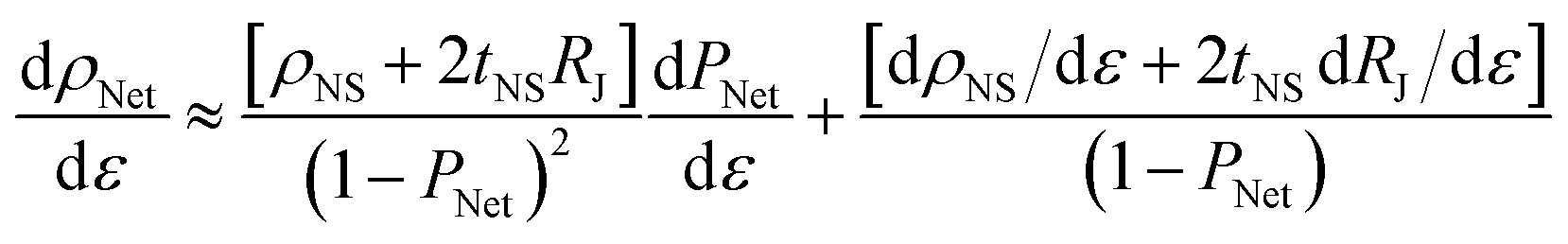 | (4) |
Substituting this result into eqn (3), leaves us with the final equation, which should describe the gauge factor of a network of conductive nanosheets in the bulklike regime.
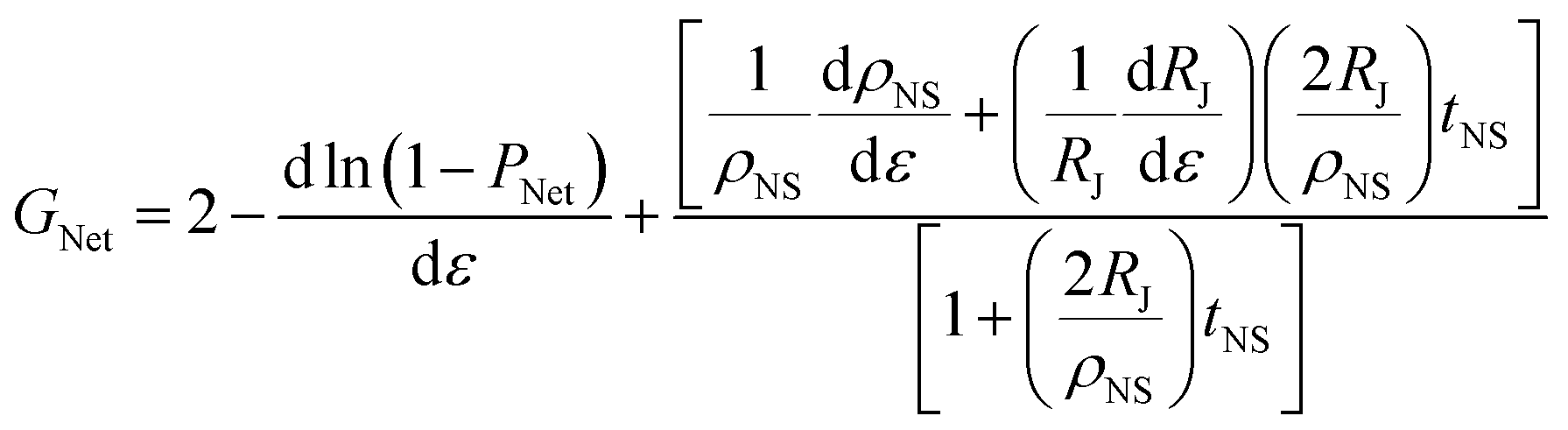 | (5) |
This equation can be used to fit data for the gauge factor, G, as a function of nanosheet thickness, outputting (dρNS/dε)/ρNS and (dRJ/dε)/RJ as fit parameters. The latter two parameters are of interest as they are linked to the gauge factors associated with individual nanosheets and individual junctions (by analogy with eqn (3)).
Model fitting
Here we fit the data in Fig. 3D using eqn (5). This equation has four fit parameters which is too many for accurate fitting to our limited data set. We can reduce the number of fit parameters by one by fixing 2RJ/ρNS = 6.13 × 10⁸ m−1 as extracted from fitting the data in Fig. 3A. However even with only three fit parameters, fitting yielded outputs with large errors. To remedy this, we attempted fitting whilst fixing the term dln(1 − PNet)/dε at various values between −2 and 2. This dramatically reduced errors while having limited impact of the remaining fit parameters (deviation of <20%). Thus, we fixed dln(1 − PNet)/dε = 0 for the remainder of the fitting. This yielded the fit shown in Fig. 3D and outputted the fit parameters (dρNS/dε)/ρNS = −13.6 ± 2.8 and (dRJ/dε)/RJ = 8.7 ± 1.1.
This fit is reasonably good for the thinner nanosheets but shows some deviation from the data for nanosheets thicker than 10 nm. This deviation is probably because one or more of the parameters in eqn (5), i.e. (dρNS/dε)/ρNS, (dRJ/dε)/RJ or dln(1 − PNet)/dε, vary slightly with nanosheet thickness (the linearity of the data in Fig. 3A implies 2RJ/ρNS does not depend on tNS). In fact, we might expect (dρNS/dε)/ρNS to be thickness independent simply because graphene nanosheets above a few layers thick tend to have thickness independent electronic properties71 and so thickness-independent ρNS. In addition, as mentioned above, RJ appears to be thickness independent implying that (dRJ/dε)/RJ might be independent of nanosheet thickness. However, it has been shown that the porosity of nanosheet networks does depend on the dimensions of the nanosheets therein.22 This implies that dln(1 − PNet)/dε might depend on nanosheet thickness. If so, this could explain the discrepancy between model and data. We demonstrate this in Fig. 3D (red dashed line) where we assume that dln(1 − PNet)/dε scales linearly with tNS as: dln(1 − PNet)/dε = −7 × 10⁷tNS while retaining the fit parameters found above. The resultant red dashed line agrees well with the entire data set. We believe this hypothesis is plausible. It is consistent with strain independent porosity for extremely thin nanosheets as originally assumed. However, for the 20 nm thick nanosheets it implies a small strain dependent porosity such that PNet changes by ∼1% for each percentage increase in strain. We believe this is reasonable.
These fit parameters are closely related to the gauge factors of individual nanosheets (GNS) and junctions (GJ). By analogy with eqn (3), we can write the gauge factor of an individual nanosheet as GNS − 2 = (dρNS/dε)0/ρNS,0, where the zero-subscripts indicate the value should be taken in the limit of low strain. This yields GNS = −11.6. ± 2.8. From the definition of gauge factor (G = (ΔR/R0)/ε, at low strain), we define the junction gauge factor as GJ = (dRJ/dε)0/RJ,0 giving GJ = 8.7 ± 1.1. These values are with respect to applied strain which to a first approximation is the same as the local strain. However, in a complex system such as this, we cannot rule out differences between local and applied strain. Further work will be required to fully address this issue. We note that because the junction gauge factor is defined in terms of an extensive property (resistance), it will depend on the size and geometry of the junctions. Thus, the value quoted here is relevant for the specific networks under study here. Further work will be required to determine how GJ depends on nanosheet type and network morphology.
The reasonably high junction gauge factor is straightforward to understand. We do expect the junctions between the nanosheets to change as we strain the network, perhaps altering the distance the charge carriers must tunnel between sheets or reducing the overlap area of the nanosheets. This has traditionally been assumed to be the dominant source of piezoresistance in nano-networks34–36 (unless the networks are very thin23).
However, the fact that we can detect the effect of strain on the nanosheet resistivity is more unexpected. For strain to have a measurable effect on the resistivity of the nanosheets within a network is surprising as we expect the sheets to slide past one another in response to external stress without themselves deforming. While there are reports on the effect of applied strain on the individual nanosheet resistances, these are for nanosheets within polymer matrices where the stress transfer is mediated by the strong matrix–nanosheet interaction.28
In addition, the fact that the nanosheet gauge factor is negative is extremely surprising. However, we could not obtain a reasonable fit without allowing a negative nanosheet gauge factor. It is known that thin graphene sheets tend to have a relatively low but positive intrinsic gauge factor of <10.72–75 However, we note that negative gauge factors have been observed for some carbon-based nanostructures. A negative piezoresistive effect was observed by Blazewicz et al. when investigating graphite fibres.76 In addition, non-carbon nanomaterials such as MoS2 have strongly negative gauge factors (GNS = −50).77
There are several possible sources of this effect, it is possible that there is some built in strain in the nanosheets as a result of forming the network, and by straining, these residual stresses are released and the nanosheets return towards a lower strain state with increasing network strain, in the limit of low strain. Alternatively, point contacts between sheets could act as scattering sites (if one sheet edge is pressed into the middle of a basal plane of another), so when the network is strained, effectively separating the sheets, and by removing this impediment, the nanosheet resistivity decreases.
Conclusion
In this study, networks of 2D graphene nanosheets were spray coated onto flexible Kapton substrates. The nanosheets used were separated from a polydisperse LPE stock solution using liquid cascade centrifugation, yielding fractions with mean nanosheet thickness ranging from ∼3 nm to ∼20 nm. By plotting network resistivity vs. nanosheet thickness, and fitting using a simple model, the nanosheet resistivity and junction resistance was determined to be ρNS = (2.9 ± 1.3) × 10−5 Ω m and RJ = 8900 ± 1000 Ω. It was observed that significant variations in the piezoresistive response occurred with changing nanosheet thickness. A physical model was derived to understand the system, which allowed us to extract the gauge factor of the nanosheets and junctions, with respect to network strain. These had values of GNS = −11.6. ± 2.8 and GJ = 8.7 ± 1.1.Methods
Graphene exfoliation
Graphite flakes (Asbury, 4 g) were sonicated for 1 h in 80 mL n-methyl-2-pyrollidone (Sigma) at 65% power with a horn probe. The suspension was centrifuged (Hettich, 10 cm radius) for 1 h at 6 kRPM. The sediment was resuspended in 80 mL of fresh NMP and sonicated for 9 h at 60% power, pulsing 4 s on 4 s off.Liquid cascade centrifugation
To size select the nanosheets, the suspension was centrifuged at 0.5 kRPM for 2 h at 5 °C. The sediment was discarded, and the supernatant was centrifuged at 1 kRPM for 2 h at 5 °C. The sediment was kept and labelled as the “0.5 to 1 kRPM” sample, (with the speeds indicating the lower and upper spin speeds used to sediment the nanosheets). The supernatant was then centrifuged at 1.5 kRPM for 2 h at 5 °C. The cycle was repeated at 2, 3, 4 and 6 kRPM, keeping the sediment each time and centrifuging the supernatant at successively higher speeds. The sediments were resuspended in fresh IPA and centrifuged at 6 kRPM for 1 h at 5 °C. Each sample was finally resuspended in fresh IPA. A schematic of this process is shown in Fig. 1A.Characterisation
The nanosheet based inks were characterised using UV-Vis spectroscopy (Cary 50), the nanosheets were spray coated on glass and characterised using Raman spectroscopy (Renishaw inVia Quantor, 532 nm). Atomic force microscopy was used to further characterise the flake thicknesses and lateral size (Digital Instruments Multimode IIIa in tapping mode AFM). Due to the measurement anomalies regularly observed in thickness measurements of liquid phase exfoliated nanosheets using AFM for a variety of materials,6,58,78–80 a previously reported and experimentally derived6 protocol was used to extract the real nanosheet thickness from the measured profiles. The conversion procedure was as follows: the measured thickness was converted to layer number by subtracting 1.0 nm to allow for trapped solvents from the measured thickness and dividing the remainder by 0.95 nm. This layer number was then multiplied by 0.35 nm (the real monolayer thickness) per layer to get the real thickness. Scanning electron microscopy of the top surface of the films was conducted using the (Zeiss) Ultra SEM operating at a potential of 3 keV, and imaging using the secondary electron detector with a working distance of 5 mm.Film deposition
Kapton substrates (DuPont Kapton HN, 125 μm) were cleaned using IPA. Compressed N2 was used to dry the samples before spray coating. The films were spray coated using a Harder & Steenbeck Infinity Airbrush, mounted in a Janome (JR2300N) mobile gantry. The gantry was rastered across a 2 cm × 4 cm area in a serpentine repeating pattern. the N2 backpressure was set to 40 PSI. The ink concentration was 0.1 mg mL−1, 50 mL of ink was sprayed for each device. Ink flow was kept constant at 50 mL h−1. The working distance from the airbrush nozzle to substrate was 10 cm.Thickness characterisation
Film thickness was measured by scanning an area of each sprayed film using an Optical Profiler (Filmetrics, Profilm3D®) with a 50× Nikon objective lens operating in the white light interferometry mode. This produced a 380 μm × 340 μm image of the film. Thickness was determined by measuring a scratched region and determining the step height from the substrate to the film surface, across the entire image using the ‘Histogram’ step height measurement on Profilm Online.Electromechanical testing
Devices were tested by contacting the networks with silver paint contacts and silver wires connected to an electrical source meter (Keithley KE2601) in a two-probe electrical test. The resistance was measured as the substrates were strained using a Zwick Z0.5 ProLine Tensile Tester with a 100 N load cell. Prior to testing, the point of zero strain, was identified by mounting the device, which is naturally slightly bent, in compression, and straining for 3 cycles up to 0.5% strain with a strain rate of 0.2% s−1 and observing the displacement at which the force increased. This displacement was used as the zero-displacement point. To verify the position a further three cycles were conducted to observe a consistent linear mechanical response before mechanical testing and cycling testing were completed.Data availability
The data supporting this article have been included as part of the ESI.†Conflicts of interest
There are no conflicts to declare.Acknowledgements
This project has received funding from the European Union's Horizon Europe research and innovation programme under grant agreement no. 101129613 (HYPERSONIC). We acknowledge the Irish Research Council (GOIPG/2020/1051) and a Marie Skłodowska-Curie Individual Fellowship “MOVE” (grant number 101030735). JM acknowledges his Margarita Salas fellowship from the Spanish Ministry of Universities. We have also received support from the Science Foundation Ireland (SFI) funded centre AMBER (SFI/12/RC/2278) and availed of the facilities of the SFI-funded advanced microscopy laboratory (AML), additive research laboratory (ARL) and iCRAG labs.References
- F. Bonaccorso, A. Bartolotta, J. N. Coleman and C. Backes, 2D-Crystal-Based Functional Inks, Adv. Mater., 2016, 28(29), 6136–6166, DOI:10.1002/adma.201506410.
- K. S. Novoselov, A. Mishchenko, A. Carvalho and A. H. Castro Neto, 2D materials and van der Waals heterostructures, Science, 2016, 353(6298), aac9439, DOI:10.1126/science.aac9439.
- K. Khan, A. K. Tareen, M. Aslam, R. Wang, Y. Zhang, A. Mahmood, Z. Ouyang, H. Zhang and Z. Guo, Recent developments in emerging two-dimensional materials and their applications, J. Mater. Chem. C, 2020, 8(2), 387–440, 10.1039/C9TC04187G.
- A. C. Ferrari, F. Bonaccorso, V. Fal'ko, K. S. Novoselov, S. Roche, P. Bøggild, S. Borini, F. H. L. Koppens, V. Palermo and N. Pugno, et al., Science and technology roadmap for graphene, related two-dimensional crystals, and hybrid systems, Nanoscale, 2015, 7(11), 4598–4810, 10.1039/C4NR01600A.
- Y. Hernandez, V. Nicolosi, M. Lotya, F. M. Blighe, Z. Sun, S. De, I. T. McGovern, B. Holland, M. Byrne and Y. K. Gun'Ko, et al., High-yield production of graphene by liquid-phase exfoliation of graphite, Nat. Nanotechnol., 2008, 3(9), 563–568, DOI:10.1038/nnano.2008.215.
- K. R. Paton, E. Varrla, C. Backes, R. J. Smith, U. Khan, A. O’Neill, C. Boland, M. Lotya, O. M. Istrate and P. King, et al., Scalable production of large quantities of defect-free few-layer graphene by shear exfoliation in liquids, Nat. Mater., 2014, 13(6), 624–630, DOI:10.1038/nmat3944.
- C. Zhi, Y. Bando, C. Tang, H. Kuwahara and D. Golberg, Large-Scale Fabrication of Boron Nitride Nanosheets and Their Utilization in Polymeric Composites with Improved Thermal and Mechanical Properties, Adv. Mater., 2009, 21(28), 2889–2893, DOI:10.1002/adma.200900323.
- J. N. Coleman, M. Lotya, A. O’Neill, S. D. Bergin, P. J. King, U. Khan, K. Young, A. Gaucher, S. De and R. J. Smith, et al., Two-Dimensional Nanosheets Produced by Liquid Exfoliation of Layered Materials, Science, 2011, 331(6017), 568–571, DOI:10.1126/science.1194975.
- D. Hanlon, C. Backes, E. Doherty, C. S. Cucinotta, N. C. Berner, C. Boland, K. Lee, A. Harvey, P. Lynch and Z. Gholamvand, et al., Liquid exfoliation of solvent-stabilized few-layer black phosphorus for applications beyond electronics, Nat. Commun., 2015, 6(1), 8563, DOI:10.1038/ncomms9563.
- A. Harvey, J. B. Boland, I. Godwin, A. G. Kelly, B. M. Szydłowska, G. Murtaza, A. Thomas, D. J. Lewis, P. O’Brien and J. N. Coleman, Exploring the versatility of liquid phase exfoliation: producing 2D nanosheets from talcum powder, cat litter and beach sand, 2D Mater., 2017, 4(2), 025054, DOI:10.1088/2053-1583/aa641a.
- C. Backes, D. Campi, B. M. Szydlowska, K. Synnatschke, E. Ojala, F. Rashvand, A. Harvey, A. Griffin, Z. Sofer and N. Marzari, et al., Equipartition of Energy Defines the Size–Thickness Relationship in Liquid-Exfoliated Nanosheets, ACS Nano, 2019, 13(6), 7050–7061, DOI:10.1021/acsnano.9b02234.
- R. Zribi, A. Foti, M. G. Donato, P. G. Gucciardi and G. Neri, Electrochemical and sensing properties of 2D-MoS2 nanosheets produced via liquid cascade centrifugation, Electrochim. Acta, 2022, 436, 141433, DOI:10.1016/j.electacta.2022.141433.
- T. Vićentić, S. Andrić, V. Rajić and M. Spasenović, Reliable fabrication of transparent conducting films by cascade centrifugation and Langmuir–Blodgett deposition of electrochemically exfoliated graphene, Beilstein J. Nanotechnol., 2022, 13, 666–674, DOI:10.3762/bjnano.13.58.
- C. Backes, B. M. Szydłowska, A. Harvey, S. Yuan, V. Vega-Mayoral, B. R. Davies, P.-L. Zhao, D. Hanlon, E. J. G. Santos and M. I. Katsnelson, et al., Production of Highly Monolayer Enriched Dispersions of Liquid-Exfoliated Nanosheets by Liquid Cascade Centrifugation, ACS Nano, 2016, 10(1), 1589–1601, DOI:10.1021/acsnano.5b07228.
- X. Huang, X. Qi, F. Boey and H. Zhang, Graphene-based composites, Chem. Soc. Rev., 2012, 41(2), 666–686, 10.1039/C1CS15078B.
- X. Sun, H. Sun, H. Li and H. Peng, Developing Polymer Composite Materials: Carbon Nanotubes or Graphene?, Adv. Mater., 2013, 25(37), 5153–5176, DOI:10.1002/adma.201301926.
- C. S. Boland, Stumbling through the Research Wilderness, Standard Methods To Shine Light on Electrically Conductive Nanocomposites for Future Healthcare Monitoring, ACS Nano, 2019, 13(12), 13627–13636, DOI:10.1021/acsnano.9b06847.
- A. G. Kelly, D. Finn, A. Harvey, T. Hallam and J. N. Coleman, All-printed capacitors from graphene-BN-graphene nanosheet heterostructures, Appl. Phys. Lett., 2016, 109(2), 023107, DOI:10.1063/1.4958858.
- F. Torrisi, T. Hasan, W. Wu, Z. Sun, A. Lombardo, T. S. Kulmala, G.-W. Hsieh, S. Jung, F. Bonaccorso and P. J. Paul, et al., Inkjet-Printed Graphene Electronics, ACS Nano, 2012, 6(4), 2992–3006, DOI:10.1021/nn2044609.
- E. Jabari and E. Toyserkani, Micro-scale aerosol-jet printing of graphene interconnects, Carbon, 2015, 91, 321–329, DOI:10.1016/j.carbon.2015.04.094.
- M. Hempel, D. Nezich, J. Kong and M. Hofmann, A novel class of strain gauges based on layered percolative films of 2D materials, Nano Lett., 2012, 12(11), 5714–5718, DOI:10.1021/nl302959a.
- C. Gabbett, L. Doolan, K. Synnatschke, L. Gambini, E. Coleman, A. G. Kelly, S. Liu, E. Caffrey, J. Munuera and C. Murphy, et al., Quantitative analysis of printed nanostructured networks using high-resolution 3D FIB-SEM nanotomography, Nat. Commun., 2024, 15(1), 278, DOI:10.1038/s41467-023-44450-1.
- E. Caffrey, J. R. Garcia, D. O’Suilleabhain, C. Gabbett, T. Carey and J. N. Coleman, Quantifying the Piezoresistive Mechanism in High-Performance Printed Graphene Strain Sensors, ACS Appl. Mater. Interfaces, 2022, 14(5), 7141–7151, DOI:10.1021/acsami.1c21623.
- A. G. Kelly, D. O’Suilleabhain, C. Gabbett and J. N. Coleman, The electrical conductivity of solution-processed nanosheet networks, Nat. Rev. Mater., 2022, 7, 217–234, DOI:10.1038/s41578-021-00386-w.
- T. Carey, O. Cassidy, K. Synnatschke, E. Caffrey, J. Garcia, S. Liu, H. Kaur, A. G. Kelly, J. Munuera and C. Gabbett, et al., High-Mobility Flexible Transistors with Low-Temperature Solution-Processed Tungsten Dichalcogenides, ACS Nano, 2023, 17(3), 2912–2922, DOI:10.1021/acsnano.2c11319.
- S. Bellani, A. Bartolotta, A. Agresti, G. Calogero, G. Grancini, A. Di Carlo, E. Kymakis and F. Bonaccorso, Solution-processed two-dimensional materials for next-generation photovoltaics, Chem. Soc. Rev., 2021, 50(21), 11870–11965, 10.1039/D1CS00106J.
- S. Liu, E.-X. Ding, A. G. Kelly, L. Doolan, C. Gabbett, H. Kaur, J. Munuera, T. Carey, J. Garcia and J. N. Coleman, Solution processed, vertically stacked hetero-structured diodes based on liquid-exfoliated WS2 nanosheets: from electrode-limited to bulk-limited behavior, Nanoscale, 2022, 14(42), 15679–15690, 10.1039/D2NR04196K.
- S. Biccai, C. S. Boland, D. P. O’Driscoll, A. Harvey, C. Gabbett, D. R. O’Suilleabhain, A. J. Griffin, Z. Li, R. J. Young and J. N. Coleman, Negative Gauge Factor Piezoresistive Composites Based on Polymers Filled with MoS2 Nanosheets, ACS Nano, 2019, 13(6), 6845–6855, DOI:10.1021/acsnano.9b01613.
- Z. Chen, L. Jin, W. Hao, W. Ren and H. M. Cheng, Synthesis and applications of three-dimensional graphene network structures, Mater. Today Nano, 2019, 5, 100027, DOI:10.1016/j.mtnano.2019.01.002.
- C. S. Boland, Performance Analysis of Solution-Processed Nanosheet Strain Sensors – A Systematic Review of Graphene and MXene Wearable Devices, Nanotechnology, 2024, 35(20), 202001, DOI:10.1088/1361-6528/ad272f.
- C. S. Boland, U. Khan, C. Backes, A. O’Neill, J. McCauley, S. Duane, R. Shanker, Y. Liu, I. Jurewicz, A. B. Dalton and J. N. Coleman, Sensitive, High-Strain, High-Rate Bodily Motion Sensors Based on Graphene–Rubber Composites, ACS Nano, 2014, 8(9), 8819–8830, DOI:10.1021/nn503454h.
- X. Li and Y. Chai, Design and applications of graphene-based flexible and wearable physical sensing devices, 2D Mater., 2020, 8(2), 022001, DOI:10.1088/2053-1583/abcbe6.
- X. Sui, J. R. Downing, M. C. Hersam and J. Chen, Additive manufacturing and applications of nanomaterial-based sensors, Mater. Today, 2021, 48, 135–154, DOI:10.1016/j.mattod.2021.02.001.
- M. Amjadi, A. Pichitpajongkit, S. Lee, S. Ryu and I. Park, Highly Stretchable and Sensitive Strain Sensor Based on Silver Nanowire–Elastomer Nanocomposite, ACS Nano, 2014, 8(5), 5154–5163, DOI:10.1021/nn501204t.
- M. Amjadi, K.-U. Kyung, I. Park and M. Sitti, Stretchable, Skin-Mountable, and Wearable Strain Sensors and Their Potential Applications: A Review, Adv. Funct. Mater., 2016, 26(11), 1678–1698, DOI:10.1002/adfm.201504755.
- J. Song, Y. Tan, Z. Chu, M. Xiao, G. Li, Z. Jiang, J. Wang and T. Hu, Hierarchical Reduced Graphene Oxide Ridges for Stretchable, Wearable, and Washable Strain Sensors, ACS Appl. Mater. Interfaces, 2019, 11(1), 1283–1293, DOI:10.1021/acsami.8b18143.
- H. Souri, H. Banerjee, A. Jusufi, N. Radacsi, A. A. Stokes, I. Park, M. Sitti and M. Amjadi, Wearable and Stretchable Strain Sensors: Materials, Sensing Mechanisms, and Applications, Adv. Intell. Syst., 2020, 2(8), 2000039, DOI:10.1002/aisy.202000039.
- A. S. Fiorillo, C. D. Critello and S. A. Pullano, Theory, technology and applications of piezoresistive sensors: A review, Sens. Actuators, A, 2018, 281, 156–175, DOI:10.1016/j.sna.2018.07.006.
- M. C. Lemme, S. Wagner, K. Lee, X. Fan, G. J. Verbiest, S. Wittmann, S. Lukas, R. J. Dolleman, F. Niklaus and H. S. J. van der Zant, et al., Nanoelectromechanical Sensors Based on Suspended 2D Materials, Research, 2020, 2020 Search PubMed.
- J. R. Garcia, M. McCrystal, D. Horváth, H. Kaur, T. Carey and J. N. Coleman, Tuneable Piezoresistance of Graphene-Based 2D:2D Nanocomposite Networks, Adv. Funct. Mater., 2023, 33(20), 2214855, DOI:10.1002/adfm.202214855.
- M. A. O’Mara, S. P. Ogilvie, M. J. Large, A. Amorim Graf, A. C. Sehnal, P. J. Lynch, J. P. Salvage, I. Jurewicz, A. A. K. King and A. B. Dalton, Ultrasensitive Strain Gauges Enabled by Graphene-Stabilized Silicone Emulsions, Adv. Funct. Mater., 2020, 30(32), 2002433, DOI:10.1002/adfm.202002433.
- Y. Yang, L. Shi, Z. Cao, R. Wang and J. Sun, Strain Sensors with a High Sensitivity and a Wide Sensing Range Based on a Ti3C2Tx(MXene) Nanoparticle–Nanosheet Hybrid Network, Adv. Funct. Mater., 2019, 29(14), 1807882, DOI:10.1002/adfm.201807882.
- C. S. Boland, U. Khan, G. Ryan, S. Barwich, R. Charifou, A. Harvey, C. Backes, Z. Li, M. S. Ferreira and M. E. Möbius, et al., Sensitive electromechanical sensors using viscoelastic graphene-polymer nanocomposites, Science, 2016, 354(6317), 1257, DOI:10.1126/science.aag2879.
- C. Casiraghi, M. Macucci, K. Parvez, R. Worsley, Y. Shin, F. Bronte, C. Borri, M. Paggi and G. Fiori, Inkjet printed 2D-crystal based strain gauges on paper, Carbon, 2018, 129, 462–467, DOI:10.1016/j.carbon.2017.12.030.
- H. Yao, M. Hempel, Y. P. Hsieh, J. Kong and M. Hofmann, Characterizing percolative materials by straining, Nanoscale, 2019, 11(3), 1074–1079, 10.1039/c8nr09120j.
- Z. Chen, T. Ming, M. M. Goulamaly, H. Yao, D. Nezich, M. Hempel, M. Hofmann and J. Kong, Enhancing the Sensitivity of Percolative Graphene Films for Flexible and Transparent Pressure Sensor Arrays, Adv. Funct. Mater., 2016, 26(28), 5061–5067, DOI:10.1002/adfm.201503674.
- J. A. Rogers, T. Someya and Y. Huang, Materials and Mechanics for Stretchable Electronics, Science, 2010, 327(5973), 1603, DOI:10.1126/science.1182383.
- M. Li, Y. Wu, L. Zhang, H. Wo, S. Huang, W. Li, X. Zeng, Q. Ye, T. Xu and J. Luo, et al., Liquid metal-based electrical interconnects and interfaces with excellent stability and reliability for flexible electronics, Nanoscale, 2019, 11(12), 5441–5449, 10.1039/C8NR09503E.
- D. P. O'Driscoll, S. McMahon, J. Garcia, S. Biccai, C. Gabbett, A. G. Kelly, S. Barwich, M. Moebius, C. S. Boland and J. N. Coleman, Printable G-Putty for Frequency- and Rate-Independent, High-Performance Strain Sensors, Small, 2021, 17(23), e2006542, DOI:10.1002/smll.202006542.
- J. R. Garcia, D. O’Suilleabhain, H. Kaur and J. N. Coleman, A Simple Model Relating Gauge Factor to Filler Loading in Nanocomposite Strain Sensors, ACS Appl. Nano Mater., 2021, 4(3), 2876–2886, DOI:10.1021/acsanm.1c00040.
- M. J. Large, S. P. Ogilvie, A. Amorim Graf, P. J. Lynch, M. A. O'Mara, T. Waters, I. Jurewicz, J. P. Salvage and A. B. Dalton, Large-Scale Surfactant Exfoliation of Graphene and Conductivity-Optimized Graphite Enabling Wireless Connectivity, Adv. Mater. Technol., 2020, 5(7), 2000284, DOI:10.1002/admt.202000284.
- T. M. Higgins, S. Finn, M. Matthiesen, S. Grieger, K. Synnatschke, M. Brohmann, M. Rother, C. Backes and J. Zaumseil, Electrolyte-Gated n-Type Transistors Produced from Aqueous Inks of WS2 Nanosheets, Adv. Funct. Mater., 2019, 29(4), 1804387, DOI:10.1002/adfm.201804387.
- C. Gabbett, A. G. Kelly, E. Coleman, L. Doolan, T. Carey, K. Synnatschke, S. Liu, A. Dawson, D. O’Suilleabhain and J. Munuera, et al., Understanding how junction resistances impact the conduction mechanism in nano-networks, Nat. Commun., 2024, 15, 4517 CrossRef CAS PubMed.
- V. Nicolosi, M. Chhowalla, G. Kanatzidis Mercouri, S. Strano Michael and N. Coleman Jonathan, Liquid Exfoliation of Layered Materials, Science, 2013, 340(6139), 1226419, DOI:10.1126/science.1226419.
- J. N. Coleman, Liquid Exfoliation of Defect-Free Graphene, Acc. Chem. Res., 2013, 46(1), 14–22, DOI:10.1021/ar300009f.
- S. Uran, A. Alhani and C. Silva, Study of ultraviolet-visible light absorbance of exfoliated graphite forms, AIP Adv., 2017, 7(3), 035323, DOI:10.1063/1.4979607.
- C. Backes, K. R. Paton, D. Hanlon, S. Yuan, M. I. Katsnelson, J. Houston, R. J. Smith, D. McCloskey, J. F. Donegan and J. N. Coleman, Spectroscopic metrics allow in situ measurement of mean size and thickness of liquid-exfoliated few-layer graphene nanosheets, Nanoscale, 2016, 8(7), 4311–4323, 10.1039/c5nr08047a.
- C. Backes, R. J. Smith, N. McEvoy, N. C. Berner, D. McCloskey, H. C. Nerl, A. O’Neill, P. J. King, T. Higgins and D. Hanlon, et al., Edge and confinement effects allow in situ measurement of size and thickness of liquid-exfoliated nanosheets, Nat. Commun., 2014, 5(1), 4576, DOI:10.1038/ncomms5576.
- A. Griffin, A. Harvey, B. Cunningham, D. Scullion, T. Tian, C.-J. Shih, M. Gruening, J. F. Donegan, E. J. G. Santos, C. Backes and J. N. Coleman, Spectroscopic Size and Thickness Metrics for Liquid-Exfoliated h-BN, Chem. Mater., 2018, 30(6), 1998–2005, DOI:10.1021/acs.chemmater.7b05188.
- G. Hu, J. Kang, L. W. T. Ng, X. Zhu, R. C. T. Howe, C. G. Jones, M. C. Hersam and T. Hasan, Functional inks and printing of two-dimensional materials, Chem. Soc. Rev., 2018, 47(9), 3265–3300, 10.1039/C8CS00084K.
- S. De, P. J. King, P. E. Lyons, U. Khan and J. N. Coleman, Size Effects and the Problem with Percolation in Nanostructured Transparent Conductors, ACS Nano, 2010, 4(12), 7064–7072, DOI:10.1021/nn1025803.
- D. McManus, S. Vranic, F. Withers, V. Sanchez-Romaguera, M. Macucci, H. Yang, R. Sorrentino, K. Parvez, S.-K. Son and G. Iannaccone, et al., Water-based and biocompatible 2D crystal inks for all-inkjet-printed heterostructures, Nat. Nanotechnol., 2017, 12(4), 343–350, DOI:10.1038/nnano.2016.281.
- S. P. Ogilvie, M. J. Large, M. A. O’Mara, A. C. Sehnal, A. Amorim Graf, P. J. Lynch, A. J. Cass, J. P. Salvage, M. Alfonso and P. Poulin, et al., Nanosheet-Stabilized Emulsions: Near-Minimum Loading and Surface Energy Design of Conductive Networks, ACS Nano, 2022, 16(2), 1963–1973, DOI:10.1021/acsnano.1c06519.
- K. H. Müller, G. Wei, B. Raguse and J. Myers, Three-dimensional percolation effect on electrical conductivity in films of metal nanoparticles linked by organic molecules, Phys. Rev. B: Condens. Matter Mater. Phys., 2003, 68(15), 155407, DOI:10.1103/PhysRevB.68.155407.
- S. De and J. N. Coleman, The effects of percolation in nanostructured transparent conductors, MRS Bull., 2011, 36(10), 774–781, DOI:10.1557/mrs.2011.236.
- A. C. Ferrari and D. M. Basko, Raman spectroscopy as a versatile tool for studying the properties of graphene, Nat. Nanotechnol., 2013, 8(4), 235–246, DOI:10.1038/nnano.2013.46.
- S. Haar, A. Ciesielski, J. Clough, H. Yang, R. Mazzaro, F. Richard, S. Conti, N. Merstorf, M. Cecchini and V. Morandi, et al., A Supramolecular Strategy to Leverage the Liquid-Phase Exfoliation of Graphene in the Presence of Surfactants: Unraveling the Role of the Length of Fatty Acids, Small, 2015, 11(14), 1691–1702, DOI:10.1002/smll.201402745.
- K. Clifford, S. P. Ogilvie, A. Amorim Graf, H. J. Wood, A. C. Sehnal, J. P. Salvage, P. J. Lynch, M. J. Large and A. B. Dalton, Emergent high conductivity in size-selected graphene networks, Carbon, 2024, 218, 118642, DOI:10.1016/j.carbon.2023.118642.
- O. Cassidy, K. Synnatschke, J. Munuera, C. Gabbett, T. Carey, L. Doolan, E. Caffrey and J. N. Coleman, Layer-by-layer assembly yields thin graphene films with near theoretical conductivity, submitted.
- S. Barwich, J. Medeiros de Araújo, A. Rafferty, C. Gomes da Rocha, M. S. Ferreira and J. N. Coleman, On the relationship between morphology and conductivity in nanosheet networks, Carbon, 2021, 171, 306–319, DOI:10.1016/j.carbon.2020.09.015.
- A. C. Ferrari, J. C. Meyer, V. Scardaci, C. Casiraghi, M. Lazzeri, F. Mauri, S. Piscanec, D. Jiang, K. S. Novoselov, S. Roth and A. K. Geim, Raman spectrum of graphene and graphene layers, Phys. Rev. Lett., 2006, 97(18), 187401, DOI:10.1103/PhysRevLett.97.187401.
- A. D. Smith, F. Niklaus, A. Paussa, S. Vaziri, A. C. Fischer, M. Sterner, F. Forsberg, A. Delin, D. Esseni and P. Palestri, et al., Electromechanical Piezoresistive Sensing in Suspended Graphene Membranes, Nano Lett., 2013, 13(7), 3237–3242, DOI:10.1021/nl401352k.
- M. Y. Huang, T. A. Pascal, H. Kim, W. A. Goddard and J. R. Greer, Electronic-Mechanical Coupling in Graphene from in situ Nanoindentation Experiments and Multiscale Atomistic Simulations, Nano Lett., 2011, 11(3), 1241–1246, DOI:10.1021/nl104227t.
- S. E. Zhu, M. K. Ghatkesar, C. Zhang and G. Janssen, Graphene based piezoresistive pressure sensor, Appl. Phys. Lett., 2013, 102(16), 161904, DOI:10.1063/1.4802799.
- M. M. Benameur, F. Gargiulo, S. Manzeli, G. Autès, M. Tosun, O. V. Yazyev and A. Kis, Electromechanical oscillations in bilayer graphene, Nat. Commun., 2015, 6(1), 8582, DOI:10.1038/ncomms9582.
- S. Blazewicz, B. Patalita and P. Touzain, Study of piezoresistance effect in carbon fibers, Carbon, 1997, 35(10), 1613–1618, DOI:10.1016/S0008-6223(97)00120-6.
- S. Manzeli, A. Allain, A. Ghadimi and A. Kis, Piezoresistivity and Strain-induced Band Gap Tuning in Atomically Thin MoS2, Nano Lett., 2015, 15(8), 5330–5335, DOI:10.1021/acs.nanolett.5b01689.
- J. Gosch, K. Synnatschke, N. Stock and C. Backes, Comparative study of sonication-assisted liquid phase exfoliation of six layered coordination polymers, Chem. Commun., 2023, 59(1), 55–58, 10.1039/D2CC03366F.
- P. Zhang, F. Zhao, P. Long, Y. Wang, Y. Yue, X. Liu, Y. Feng, R. Li, W. Hu, Y. Li and W. Feng, Sonication-assisted liquid-phase exfoliated α-GeTe: a two-dimensional material with high Fe3+ sensitivity, Nanoscale, 2018, 10(34), 15989–15997, 10.1039/C8NR03091J.
- K. Synnatschke, S. Shao, J. van Dinter, Y. J. Hofstetter, D. J. Kelly, S. Grieger, S. J. Haigh, Y. Vaynzof, W. Bensch and C. Backes, Liquid Exfoliation of Ni2P2S6: Structural Characterization, Size-Dependent Properties, and Degradation, Chem. Mater., 2019, 31(21), 9127–9139, DOI:10.1021/acs.chemmater.9b03468.
Footnote |
| † Electronic supplementary information (ESI) available. See DOI: https://doi.org/10.1039/d4nh00224e |
| This journal is © The Royal Society of Chemistry 2024 |