
 Open Access Article
 This Open Access Article is licensed under a Creative Commons Attribution-Non Commercial 3.0 Unported Licence
Resistive switching memories with enhanced durability enabled by mixed-dimensional perfluoroarene perovskite heterostructures†
Michalis
Loizos
a,
Konstantinos
Rogdakis
 *ab,
Weifan
Luo
c,
Paul
Zimmermann
d,
Alexander
Hinderhofer
d,
Jovan
Lukić
c,
Marinos
Tountas
a,
Frank
Schreiber
d,
Jovana V.
Milić
*c and
Emmanuel
Kymakis
*ab
*ab,
Weifan
Luo
c,
Paul
Zimmermann
d,
Alexander
Hinderhofer
d,
Jovan
Lukić
c,
Marinos
Tountas
a,
Frank
Schreiber
d,
Jovana V.
Milić
*c and
Emmanuel
Kymakis
*ab
aDepartment of Electrical & Computer Engineering, Hellenic Mediterranean University (HMU), Heraklion 71410, Crete, Greece. E-mail: krogdakis@hmu.gr; kymakis@hmu.gr
bInstitute of Emerging Technologies (i-EMERGE) of HMU Research Center, Heraklion 71410, Crete, Greece
cAdolphe Merkle Institute, University of Fribourg, Fribourg 1700, Switzerland. E-mail: jovana.milic@unifr.ch
dInstitute of Applied Physics, University of Tübingen, Tübingen 72076, Germany
First published on 20th May 2024
Abstract
Hybrid halide perovskites are attractive candidates for resistive switching memories in neuromorphic computing applications due to their mixed ionic-electronic conductivity. Moreover, their exceptional optoelectronic characteristics make them effective as semiconductors in photovoltaics, opening perspectives for self-powered memory elements. These devices, however, remain unexploited, which is related to the variability in their switching characteristics, weak endurance, and retention, which limit their performance and practical use. To address this challenge, we applied low-dimensional perovskite capping layers onto 3D mixed halide perovskites using two perfluoroarene organic cations, namely (perfluorobenzyl)ammonium and (perfluoro-1,4-phenylene)dimethylammonium iodide, forming Ruddlesden–Popper and Dion–Jacobson 2D perovskite phases, respectively. The corresponding mixed-dimensional perovskite heterostructures were used to fabricate resistive switching memories based on perovskite solar cell architectures, showing that the devices based on perfluoroarene heterostructures exhibited enhanced performance and stability in inert and ambient air atmosphere. This opens perspectives for multidimensional perovskite materials in durable self-powered memory elements in the future.
New conceptsHybrid organic–inorganic metal halide perovskites have become promising materials in resistive switching memories for neuromorphic computing. Moreover, their power conversion efficiency in photovoltaics provided an unprecedented opportunity for the development of self-powered brain-inspired memory technologies. However, this innovative potential has not been realized due to the instabilities of hybrid halide perovskites under resistive switching operating conditions that compromise their durability in the corresponding memory devices. In this work, we demonstrate a new concept for enhancing the durability of resistive switching perovskite memories by applying perfluoroarene-based low-dimensional perovskite capping layers onto 3D metal halide perovskites comprising (perfluorobenzyl)ammonium and (perfluoro-1,4-phenylene)dimethylammonium iodide species that form Ruddlesden–Popper and Dion–Jacobson layered (2D) perovskite phases, respectively. This provides access to mixed-dimensional perfluoroarene-based perovskite heterostructures that have been applied to resistive switching memories based on perovskite solar cell architectures, which exhibit enhanced performance and stability as compared to conventional perovskite resistive switching memory devices. This advancement highlights the potential of multidimensional perovskite materials for durable and self-powered memory elements in the future. |
Introduction
Resistive switching memories have emerged as innovative devices that provide benefits due to switching speed,1 cycling endurance, and state retention,2,3 as well as extended scalability4 compatible with executing computation tasks at low power consumption.5,6 Such non-von Neumann computing architectures enabled by resistive switching memories (often referred to as ‘memristors’) could offer local learning and decision-making functions,7–9 aiming to provide brain-inspired in-memory processing with high energy efficiency.10 Resistive switching memories have also been used as artificial synapses and neurons for neural networks,11,12 implemented through memristive crossbar arrays,13 which could overcome conventional computing architecture power limitations for the future of electronics.14,15 To this end, oxide-based memristors provided superior state-of-the-art performance in resistive memories.16 Other materials have also been used, including 2D17 and organic materials.18 Recently, metal halide perovskites have been identified as promising materials that possess unique optoelectronic properties and accessible solution-processed manufacturing at lower temperatures that are compatible with flexible substrates,19 extending their application beyond photovoltaics.20–25 They are based on AMX3 formulae comprising divalent metals (M, mostly Pb2+) and halide anions (X = I, Br, Cl) in a corner-sharing octahedral framework hosting central (A) cations (e.g., Cs, Rb, methylammonium (MA), formamidinium (FA), etc.). In a typical perovskite solar cell, hysteresis is observed in current–voltage characteristics, which is associated with ion migration processes.26,27 Such mixed ionic-electronic conductivity can be detrimental to solar cell operation; however, it is relevant in resistive switching,28 suggesting their potential use in ‘memristive’ devices.29 High-performance resistive switching memories based on halide perovskites have shown low voltage operation,30 high ON/OFF ratios,31 long retention,32 and fast switching speed.33 Moreover, lead-free compounds were also used in more sustainable memories.34,35 The underlying ion migration across halide perovskite compositions was associated with both cation and halide mobility upon external stimulation, such as electric fields and light illumination.36–39 Other defects in halide perovskites, including vacancies, interstitials, and cation substitutions, can contribute to the ion migration process. The activation energy for migration of iodine vacancies (VI) is ∼0.1 eV and is much lower compared to MA (VMA) and Pb (VPb) vacancies, which are around 0.46 eV and 0.8 eV, respectively.40,41 Accordingly, halide ions can drift under an electric field and diffuse due to concentration gradients, and the redistribution can lead to the formation of conductive filaments at the onset of a resistive switch.42 The formation and rupture of such conductive filaments of metal ions or halide vacancies between contact electrodes is the most widely accepted mechanism of operation for halide perovskite resistive switches.43–45 However, additional mechanisms may affect the resistive switching, such as the presence of interfacial Schottky barriers or trap-controlled space charge limited currents.46,47These processes are sensitive to environmental conditions, such as oxygen and moisture, which can compromise the durability of perovskite devices, necessitating alternative stabilisation strategies.48,49 To address this, layered (2D) halide perovskites that incorporate organic spacer layers between perovskite slabs in either Ruddlesden Popper50 (RP) or Dion–Jacobson (DJ)51 phases have been applied to resistive switching devices.52–54 It was shown that their use in 2D/3D perovskite heterostructures can enhance the efficiency of perovskite devices24 due to defect passivation at the interface55 or bulk,56,57 as well as between the perovskite and the transport layers.58,59 Moreover, hydrophobic organic spacers improve the ambient and operational stability of materials and devices.60 While 2D/3D perovskite heterostructures have been applied to resistive switching,61–63 a limited number of reports address the effect of dimensionality and mixed-dimensional perovskite heterostructures on the resistive switching characteristics, and this approach remains unexploited in solar cell architectures despite their potential for self-powered memories.
In this study, we apply hydrophobic perfluoroarene cations, namely (perfluorobenzyl)ammonium (F-BNA) and (perfluoro-1,4-phenylene)dimethylammonium (F-PDMA) iodide, which can form RP and DJ layered (2D) perovskite phases,64 respectively, on the surface of mixed halide perovskite thin films in solar cell memory devices (Fig. 1a). We demonstrate the formation of mixed-dimensional perovskite heterostructures and investigate their effect on device performance and stability, showing that both systems improve endurance and retention compared to the control devices. The F-BNA-based RP system displayed a prolonged cycling endurance of 104 and retention time of 5 × 10³ s, whereas the F-PDMA-based DJ perovskite devices had an endurance of 5 × 10³ cycles and retention time of 3 × 10³ s, compared to the cycling endurance and retention of 1.2 × 10³ cycles and 1.2 × 10³ s for the control device. Moreover, mixed-dimensional perovskite devices featured stability over three months in an inert atmosphere and over one month in ambient conditions, highlighting the beneficial effect of perfluoroarenes on the durability of memory devices.
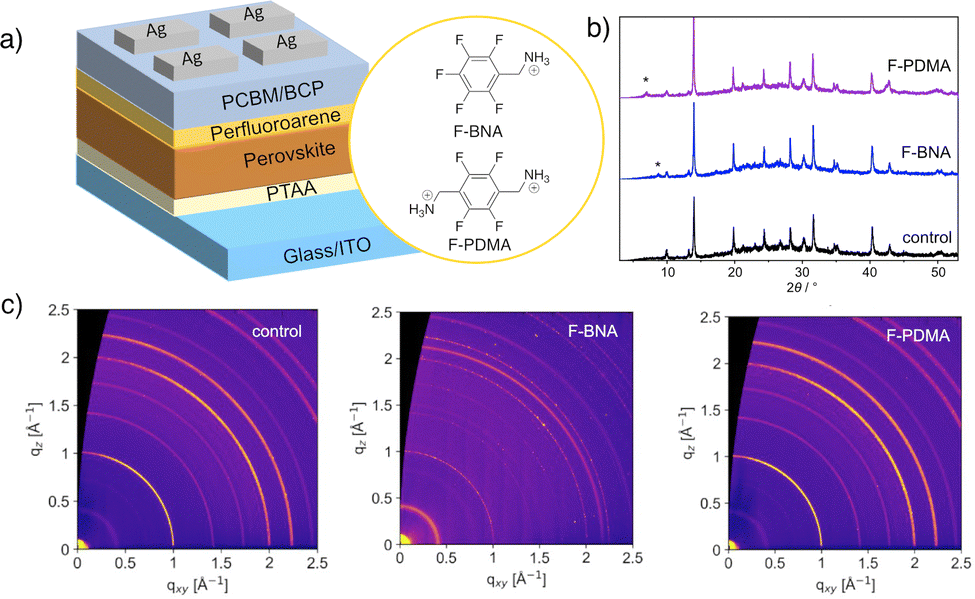 | ||
| Fig. 1 Mixed-dimensional heterostructures in resistive switching memory. (a) Schematic of perovskite solar cell memory device incorporating perfluoroarene-based mixed-dimensional perovskite heterostructures with the structure of the corresponding organic spacers used (F-BNA and F-PDMA). PCBM = [6,6]-phenyl-C61-butyric acid methyl ester; BCP = bathocuproine; PTAA = poly(triarylamine); ITO = indium-doped tin oxide. Cross-sectional images of devices are shown in Fig. S3 (ESI†). (b) X-ray diffraction patterns of control (black), F-BNAI (blue, 6 mg ml−1), and F-PDMAI2 (purple, 3 mg ml−1) treated perovskite films; lower angle reflections (asterisk) correspond to the low-dimensional perovskite phases. (c) GIWAXS data of control, F-BNAI (1 mg ml−1), and F-PDMAI2 (2 mg ml−1) treated perovskite films on glass slides measured at an angle of incidence 0.14°. Radial profiles extracted from GIWAXS data are shown in Fig. S1 of the ESI.† | ||
Results and discussion
Perfluoroarene systems, F-PDMAI2 and F-BNAI,64 were applied as overlayers to (FAMA)0.91Cs0.05Rb0.04Pb(I0.85Br0.15)3 perovskite compositions to form 2D/3D perovskite heterostructures (Fig. 1b). For this purpose, precursor salts of different concentrations (1–6 mg ml−1) were dissolved in isopropyl alcohol and spin-coated, followed by annealing at 100 °C for 5 min (as detailed in the Experimental section of ESI†).Mixed-dimensional perovskite heterostructures were analysed by X-ray diffraction (XRD) of the films, revealing low-angle reflections below 2θ of 10° (Fig. 1b) that correspond to the low-dimensional perovskite phases. Wide-angle X-ray scattering (GIWAXS) measurements revealed the presence of Bragg peaks with q < 1 Å−1 (Fig. S1, ESI†), including an additional signal at approximately 0.5 Å in the case of F-PDMAI2-treated perovskite thin films, even at lower concentrations (1–3 mg ml−1; Fig. 1b and c), corresponding to a low-dimensional phase without preferential orientation (Fig. S1, ESI†). The comparison of the peak positions to the corresponding 2D RP and DJ phases (Fig. S1, ESI†)64 suggests the formation of 2D/3D perovskite heterostructures, while co-existence of other low-dimensional perovskite phases could not be excluded under these conditions. This was further in accordance with the UV-vis absorption spectra (Fig. S2, ESI†), revealing comparable spectral characteristics at lower concentrations (1 mg ml−1), with changes in the spectral offset at higher concentrations (5 mg ml−1) for both systems (Fig. S2, ESI†). The presence of the overlayer had no significant effect on the bandgap (Eg) of the control films (1.56 eV), slightly reducing Eg for both F-BNAI (1.54 eV) and F-PDMAI2 (1.53 eV), with pronounced effects in higher concentrations, corroborating the formation of a mixed-dimensional heterostructure.
The morphology of the films was further investigated by atomic force microscopy (AFM; Fig. S4, ESI†), revealing changes upon deposition of the overlayer, which was reflected in the formation of uniform thin films without pinholes. Moreover, the presence of perfluoroarene moieties was found to increase the surface hydrophobicity, as demonstrated by contact angle measurements with a water droplet (Fig. S5, ESI†). Both F-PDMAI2 (49.2°) and F-BNAI (55.0°) treated perovskite films were more hydrophobic than the control (40.5°), suggesting the potential of mixed-dimensional heterostructures to improve the stability against moisture in perovskite materials and devices. The effects were further investigated in conventional indium-doped tin oxide glass (ITO)/poly(triarylamine)(PTAA)/perovskite/perfluoroarene/[6,6]-phenyl-C61-butyric acid methyl ester (PCBM)/bathocuproine (BCP)/Ag solar cell device architectures (Fig. 1a), which have previously shown potential to operate as memories.65–70
Steady-state resistive switching characteristics
To assess the resistive switching behaviour, we examined the steady-state current–voltage (I–V) characteristics of 30 control and treated devices (Fig. 2a–i) and determined their ON/OFF ratio between high resistance state (HRS) and low resistance state (LRS) currents, as well as SET (VSET) and RESET (VRESET) voltages. We also included in our analysis the variation coefficient (CV), defined as the percentage ratio of the standard deviation (σ) divided by the median values (μ), to evaluate the dispersion of switching voltages around their average values for cycle-to-cycle variations in devices. The control resistive switching memory showed stable, bipolar characteristics with an ON/OFF ratio in the order of 103, within an operation window below 1 V (Fig. 2a and d). The HRS current was at 10−7A, whereas the LRS current is on the order of 10−3 A. The average VSET and VRESET voltage for 30 I–V sweeps (Fig. 2d and g) was found to be 0.22 ± 0.07 V (34%) and −0.68 ± 0.11 V (16%), respectively. To identify optimal conditions for F-BNAI and F-PDMAI2, we tested a range of spacer concentrations (1–5 mg ml−1) and monitored the device characteristics (Fig. 2b and c).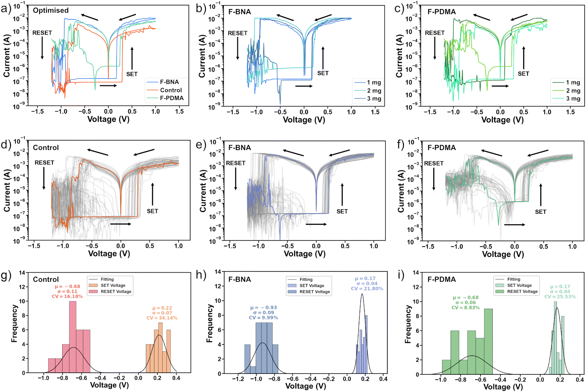 | ||
| Fig. 2 Steady-state resistive switching memory characteristics. (a)–(c) Current–voltage (I–V) characteristics of (a) control, (b) F-BNAI and (c) F-PDMAI2 treated devices with different spacer concentrations (1–3 mg ml−1) and (a) optimised preparation conditions (1 mg ml−1 for F-BNAI and 2 mg ml−1 for F-PDMAI2 treated devices). (d)–(f) I–V characteristics of 30 (d) control, (e) F-BNAI and (f) F-PDMAI2 devices under optimised preparation conditions. (g)–(i) Switching voltage distribution and statistics for the (g) control and optimised (h) F-BNAI and (i) F-PDMAI devices. CV represents the variation coefficient defined as the ratio of the standard deviation (σ) divided by the median values (μ) to estimate the dispersion of switching voltages in cycle-to-cycle switching variations. Characteristics for treated devices of other concentrations of F-BNAI and F-PDMAI2 are shown in Fig. S6–S8 of the ESI.† | ||
Steady-state I–V curves for F-PDMAI2-treated perovskite devices (Fig. 2f and i and Fig. S6, ESI†) demonstrated stable, bipolar resistive switching with a similar ON/OFF ratio as the control device within a comparable operational window of <1 V. Similarly, F-BNAI-treated devices (Fig. 2e and h and Fig. S6, ESI†) exhibited bipolar resistive switching below 1 V with a comparable ON/OFF ratio and the average VSET slightly higher compared to the control devices (Fig. 2a and Fig. S7, ESI†). However, increasing the concentration to 5 mg ml−1 (Fig. S8, ESI†) led to the absence of resistive switching for both systems, likely due to a thick low-dimensional perovskite overlayer that could affect the conductive filament formation.62 Moreover, the variation coefficient was reduced for lower concentrations of the perfluoroarene (1 mg ml−1 F-BNAI and 2 mg ml−1 F-PDMAI2), suggesting a better cycle-to-cycle variation that is relevant for improving the device reproducibility (Fig. S7, ESI†). This defines the optimal conditions (a summary of VSET AND VRESET values for each case can be found in Table S1, ESI†). The optimised conditions (Fig. 2a) were thereafter applied in the devices used for further evaluation of their resistive switching endurance, state retention, as well as the overall stability during operation that is relevant to their application.
Resistive switching endurance and state retention
The cycling endurance (Fig. 3a–d) of the devices was further evaluated using electrical pulses of the same waveform of ±1 V amplitude and 100 ms duration for the writing and erase pulses and 20 mV for 2 ms for the reading pulse (Fig. 3a, left). The cycling endurance tests of the control device (Fig. 3b) revealed a maintained ON/OFF ratio over approximately 103 cycles before the device LRS abruptly transitioned to the HRS irreversibly. The intermediate points that appear in the endurance plots are likely the result of insufficient formation/rupture of the conductive filament in the resistive switching process.71 The resistance state retention was measured using a ±1 V pulse of 4 s duration followed by reading at 20 mV for every 5 s (Fig. 3a, right). Under these conditions, the control device maintained both resistance states for 1.2 × 10³ s (Fig. 3e) before a transition from LRS to HRS took place.72,73 In contrast, optimised F-PDMAI2 devices (2 mg ml−1) featured a higher endurance of 5 × 10³ cycles without reduction in the ON/OFF ratio (Fig. 3c) and with the state retention (Fig. 3f) of 2.3 × 10³ s. Alternative F-PDMAI2 concentrations of 1 and 3 mg ml−1 resulted in a lower endurance of 5 × 10² and 4 × 10³ cycles (Fig. S10, ESI†) with the state retention of 5 × 10² and 2.3 × 10³ s (Fig. S9, ESI†), respectively. Instead, the optimal performance of the F-BNAI treated devices was superior in lower concentrations (1 mg ml−1), which is likely the result of a more insulating character of the spacer cation and its preferential bilayer formation in 2D RP phases (Fig. 3d and Fig. S9, ESI†). The optimal F-BNAI devices showed a cycling endurance of 104 cycles without any reduction of the ON/OFF ratio, which is almost an order of magnitude higher than that of the control device. The corresponding retention characteristics were also superior, as devices maintained their HRS for 5 × 10³ s, whereas the LRS increased from 300 Ω to 1 kΩ after 5 × 10³ s, which was significantly higher as compared to the control devices (Fig. 3g). In contrast, higher concentrations of F-BNAI (2 and 3 mg ml−1) led to a slightly lower endurance of 2.9 × 10³ and 2.3 × 10³ cycles (Fig. S10, ESI†), with the retention of 6.6 × 10² s and 3.6 × 10³ s, respectively (Fig. S9, ESI†). This highlights the superior performances of F-BNAI-treated devices in optimal lower concentrations as compared to F-PDMAI2 and control devices (Table S2, ESI†). Moreover, both spacers featured competitive performance as compared to the state-of-the-art hybrid perovskite resistive switching memories to date (Table S3, ESI†).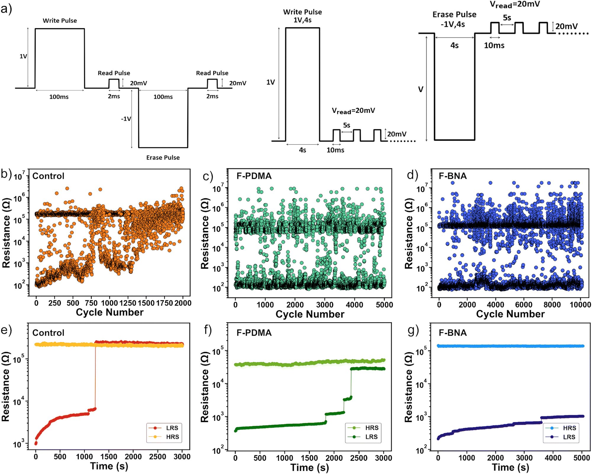 | ||
| Fig. 3 Resistive switching cycling endurance and state retention. (a) Electrical pulse waveforms were used for the cycling endurance (left) and state retention (right) measurements throughout the study. (b)–(d) Cycling endurance and (e)–(g) state retention plots of the (b) and (e) control and (c) and (f) optimised F-PDMAI2 (2 mg ml−1) and (d) and (g) F-BNAI (1 mg ml−1) treated devices. The resistive switching characteristics of F-BNAI and F-PDMAI2 treated devices of other concentrations (1–3 mg ml−1) are shown in Fig. S9–S10 of the ESI.† | ||
Device stability
The stability of the control, F-BNAI- and F-PDMAI2-treated resistive switching devices were evaluated by monitoring their characteristics in both inert and ambient environment conditions over three and one-month periods, respectively. I–V curves of the control and optimal F-BNAI and F-PDMAI2 treated devices were recorded in one-month intervals upon storage under an inert nitrogen atmosphere in the dark for a total period of three months (Fig. 4a–c and Fig. S11, ESI†). All values for the ON/OFF ratio calculation were extracted at 50 mV at LRS and HRS, and the evolution of parameters over time is detailed in Table S4 (ESI†). The control devices during the first month featured an average VSET, VRESET, and ON/OFF ratio of 0.27 ± 0.06 V, −0.53 ± 0.04 V, and 2.95 × 10², respectively. After three months, the resistive behaviour was no longer observed, and the control device failed to maintain its switching characteristics (Fig. 4a). In contrast, the F-BNAI-treated device had a VSET, VRESET, ON/OFF ratio of 0.30 ± 0.03 V, −0.60 ± 0.08 V, and 4.46 × 10² during the first month of storage, whereas after three months, the parameters were maintained at 0.21 ± 0.04 V, −0.77 ± 0.06 V, and 2.50 × 10³ (Fig. 4c), respectively, demonstrating the ability of the perfluoroarenes to prolong the device lifetime without significant deterioration. Similarly, F-PDMAI2-treated devices during the first month of storage (Fig. 4b) exhibited an average VSET of 0.16 ± 0.06 V, VRESET of −0.79 ± 0.23 V, with the ON/OFF ratio of 1.01 × 10³. During the second month of storage, these values were 0.26 ± 0.08 V, −0.79 ± 0.23 V, and 1.42 × 10², respectively, and the parameters remained comparable after the third month with an average VSET, VRESET, and ON/OFF ratio of 0.14 ± 0.03 V, −0.71 ± 0.07 V, and 2.33 × 10³, respectively. Accordingly, both perfluoroarene systems outperformed the control devices in terms of shelf-life stability under an inert atmosphere.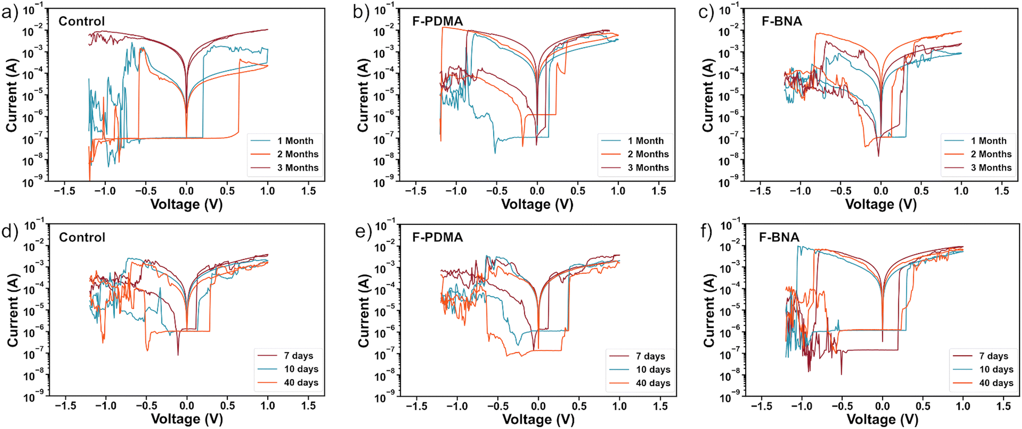 | ||
| Fig. 4 Resistive switching device stability. I–V characteristics of the devices (a)–(c) for 3 months under inert atmosphere and (d)–(f) for 40 days in ambient air, including control (a) and (d), F-PDMAI2 (b) and (e) and F-BNAI (c) and (f) treated devices. Complementary device stability is shown in Fig. S11 and S12 of the ESI.† | ||
The ambient stability of devices was thereafter investigated by monitoring the I–V parameters during an exposure period of 40 days in a humid ambient environment without any encapsulation (relative humidity 40–60%; Fig. S12 and Table S5, ESI†). The control device deteriorated already after 7 days of air exposure (Fig. 4d). In the case of F-PDMAI2-treated devices (Fig. 4e), the VSET, VRESET, and ON/OFF ratio decreased slightly after 40 days, and the device remained functional. Similarly, F-BNAI treated systems (Fig. 4f), retained their performance after 40 days of exposure, with the highest ON/OFF ratio compared to the control and F-PDMAI2 devices. This suggests that both perfluoroarene systems enhance durability, whereas F-BNAI-treated devices are more reliable, even after 40 days of ambient air exposure. The reduction of the ON/OFF ratio can be ascribed to the humidity-induced degradation,74 which can be suppressed by using the hydrophobic materials at the interface, contributing to the enhancement of the overall stability. The ambient stability results agree with the wetting properties of the perovskite films with and without perfluoroarene treatment, highlighting the potential of perfluoroarenes to sustain device operation under ambient conditions.
Conduction mechanism
A commonly accepted mechanism of conduction for halide perovskite resistive switching devices is the formation and rupture of conductive filaments of halide vacancies or metal cations,45,75–81 which is affected by the choice of electrode.82–84 Upon illumination, a decrease in the LRS current due to VI/VIX recombination process results in conductive filament annihilation.85–90 Such abrupt switching can also be the result of conductive bridges between the electrodes through either halide (either I or Br) vacancies or metal cations upon electrochemical metallisation. For halide perovskite resistive switches in the initial state, halide vacancies are randomly distributed in the perovskite layer without preferential orientation. After the application of positive voltage on the top electrode (Ag), metal ions can migrate through the perovskite layer, whereas halide ions drift and their vacancies migrate in the opposite direction (Fig. 5). When the threshold SET voltage is reached, conductive paths are formed between the two electrodes (Ag and ITO, Fig. 1a). When negative voltage is applied to the Ag top electrode, a threshold RESET voltage can be reached and the conductive filament ruptures as halide ions are now drifting towards the bottom electrode, filling the vacancies,91 leading to the transition to the HRS.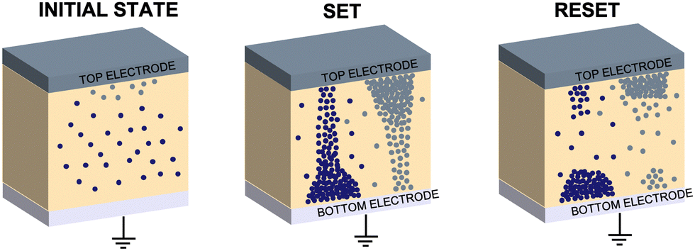 | ||
| Fig. 5 Resistive switching mechanism. Schematic of the resistive switching of halide perovskite memory devices, indicating the formation (SET) and rupture (RESET) of the conductive filaments (ion vacancies in blue and metal cations in grey). The perovskite layer is represented in light orange. | ||
To assess the mechanism that governs such resistive switching process in mixed-dimensional halide perovskite memory devices, we performed further investigation of the I–V characteristics of the devices based on F-PDMAI2 and F-BNAI systems and compared them to the control by performing space-charge-limited current (SCLC) analysis (Fig. S13, ESI†). All three systems showed a linear relationship between I and 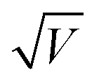 , which is indicative of Schottky emission conduction that can be described by the following equation92–94
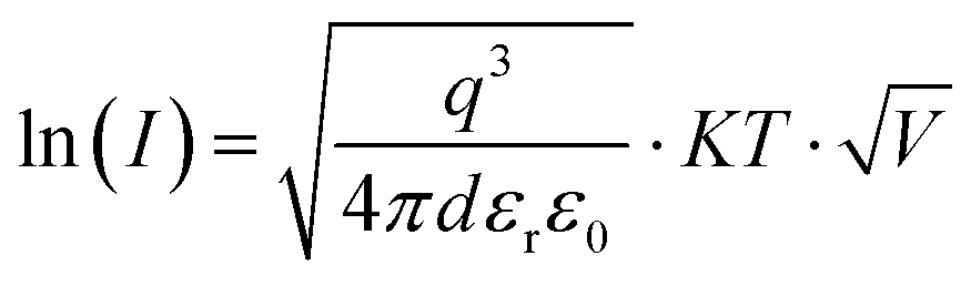 , where q is the elementary charge, ε0 and εr vacuum and material relative permittivity, k Boltzmann's constant, d dielectric layer thickness and T temperature. The slope for the control device was 0.97, close to unity, thus indicating ohmic conduction. The same analysis was performed upon F-BNAI and F-PDMAI2 treatment, revealing LRS slopes of 1.04 and 1.07, respectively. Accordingly, the perfluoroarene resistive switching memory devices were found to exhibit ohmic conduction in the LRS as well. A comparable analysis was performed for the case of HRS for all three systems (Fig. S13, ESI†), demonstrating analogous behaviour, which corroborates the filamentary switching mechanism that could be stabilised in perfluoroarene mixed-dimensional heterostructures, providing a versatile strategy that stimulates future investigations.
Conclusions
In summary, we employed two perfluoroarene systems based on (perfluorobenzyl)ammonium (F-BNA) and (perfluoro-1,4-phenylene)dimethylammonium (F-PDMA) iodides, which form Ruddlesden–Popper and Dion–Jacobson perovskite phases, respectively, at the interface with the 3D perovskite layer in photovoltaic devices. We demonstrated mixed-dimensional heterostructures that display resistive switching memory behaviour with the enhancement of the performance and endurance in inert and ambient environments. The F-BNA-based system showed a prolonged cycling endurance of 104 and retention time of 5 × 10³ s, whereas the F-PDMA-based devices had an endurance of 5 × 10³ cycles and retention time of 3 × 10³ s, compared to the 1.2 × 10³ cycles and 1.2 × 10³ s for control devices. This advancement highlights the potential of mixed-dimensional perovskites in self-powered memories.Data availability
Data can be accessed at the DOI: 10.5281/zenodo.11134559 and it is available under the license CC-BY-4.0.Author contributions
The study was conceptualized by K. R. with the support of J. V. M. and E. K., who directed the project, whereas M. L. led the experimental effort, analysis, and manuscript writing under the supervision of K. R. and the support of M. T. in precursor solution preparation and AFM measurements. The synthesis and characterization of perfluoroarenes and their films were performed by W. L. and J. L. under the supervision of J. V. M. X-ray scattering measurements and analysis were conducted by P. Z. under the supervision of A. H. and F. S. All authors contributed to the discussion and the final version of the manuscript.Conflicts of interest
There are no conflicts to declare.Acknowledgements
The work has been supported by the European Union's Horizon 2020 research and innovation program under project EMERGE (grant agreement no. 101008701) and the National Foundation for Research and Innovation under project INTELLECT (no. 81045). W. L. and J. V. M. acknowledge the support of the Swiss National Science Foundation project no. 193174 and the Adolphe Merkle Institute (AMI) as well as NCCR Bio-Inspired Materials program at the University of Fribourg in Switzerland. They are grateful to Patricia A. Gaina and Ethan Lim (AMI) for the procedure for the synthesis of perfluoroarenes, Dr Gianluca Bravetti (AMI) for support with SEM measurements at AMI, and Ghewa AlSabeh (EPFL) for her support with the X-ray scattering measurements. J. L. is grateful for the support of the research exchange fellowship at the University of Fribourg in Switzerland and his advisor, Dr Vuk Radmilović, for mentorship and support. P. Z., A. H., and F. S. would like to thank BMBF for financial support. Finally, the authors acknowledge the support of Andrea Resta and Alessandro Coati from the beamline SIXS at the synchrotron SOLEIL (proposal no. 20191295) in France.References
- M.-J. Lee, C. B. Lee, D. Lee, S. R. Lee, M. Chang, J. H. Hur, Y.-B. Kim, C.-J. Kim, D. H. Seo, S. Seo, U.-I. Chung, I.-K. Yoo and K. Kim, Nat. Mater., 2011, 10, 625–630 CrossRef CAS PubMed.
- J. J. Yang, M.-X. Zhang, J. P. Strachan, F. Miao, M. D. Pickett, R. D. Kelley, G. Medeiros-Ribeiro and R. S. Williams, Appl. Phys. Lett., 2010, 97, 232102 CrossRef.
- S. Chakrabarti, D. Jana, M. Dutta, S. Maikap, Y.-Y. Chen and J.-R. Yang, in 2014 IEEE 6th International Memory Workshop (IMW), 2014, pp. 1–4 Search PubMed.
- B. Govoreanu, G. S. Kar, Y.-Y. Chen, V. Paraschiv, S. Kubicek, A. Fantini, I. P. Radu, L. Goux, S. Clima, R. Degraeve, N. Jossart, O. Richard, T. Vandeweyer, K. Seo, P. Hendrickx, G. Pourtois, H. Bender, L. Altimime, D. J. Wouters, J. A. Kittl and M. Jurczak, in 2011 International Electron Devices Meeting, 2011, pp. 31.6.1–31.6.4 Search PubMed.
- B. Gao, Y. Bi, H.-Y. Chen, R. Liu, P. Huang, B. Chen, L. Liu, X. Liu, S. Yu, H.-S. P. Wong and J. Kang, ACS Nano, 2014, 8, 6998–7004 CrossRef CAS PubMed.
- L. Xu, R. Yuan, Z. Zhu, K. Liu, Z. Jing, Y. Cai, Y. Wang, Y. Yang and R. Huang, Adv. Mater. Technol., 2019, 4, 1900212 CrossRef CAS.
- M. Lanza, A. Sebastian, W. D. Lu, M. Le Gallo, M.-F. Chang, D. Akinwande, F. M. Puglisi, H. N. Alshareef, M. Liu and J. B. Roldan, Science, 2022, 376, eabj9979 CrossRef CAS PubMed.
- A. Mehonic, A. Sebastian, B. Rajendran, O. Simeone, E. Vasilaki and A. J. Kenyon, Adv. Intell. Syst., 2020, 2, 2000085 CrossRef.
- H.-L. Park, Y. Lee, N. Kim, D.-G. Seo, G.-T. Go and T.-W. Lee, Adv. Mater., 2020, 32, 1903558 CrossRef CAS PubMed.
- M. A. Zidan, J. P. Strachan and W. D. Lu, Nat. Electron., 2018, 1, 22–29 CrossRef.
- P.-X. Chen, D. Panda and T.-Y. Tseng, Sci. Rep., 2023, 13, 1454 CrossRef CAS PubMed.
- L. Chen, T.-Y. Wang, Y.-W. Dai, M.-Y. Cha, H. Zhu, Q.-Q. Sun, S.-J. Ding, P. Zhou, L. Chua and D. W. Zhang, Nanoscale, 2018, 10, 15826–15833 RSC.
- C. Li, M. Hu, Y. Li, H. Jiang, N. Ge, E. Montgomery, J. Zhang, W. Song, N. Dávila, C. E. Graves, Z. Li, J. P. Strachan, P. Lin, Z. Wang, M. Barnell, Q. Wu, R. S. Williams, J. J. Yang and Q. Xia, Nat. Electron., 2018, 1, 52–59 CrossRef.
- M. Kimura, Y. Shibayama and Y. Nakashima, Sci. Rep., 2022, 12, 5359 CrossRef CAS PubMed.
- D. V. Christensen, R. Dittmann, B. Linares-Barranco, A. Sebastian, M. L. Gallo, A. Redaelli, S. Slesazeck, T. Mikolajick, S. Spiga, S. Menzel, I. Valov, G. Milano, C. Ricciardi, S.-J. Liang, F. Miao, M. Lanza, T. J. Quill, S. T. Keene, A. Salleo, J. Grollier, D. Marković, A. Mizrahi, P. Yao, J. J. Yang, G. Indiveri, J. P. Strachan, S. Datta, E. Vianello, A. Valentian, J. Feldmann, X. Li, W. H. P. Pernice, H. Bhaskaran, S. Furber, E. Neftci, F. Scherr, W. Maass, S. Ramaswamy, J. Tapson, P. Panda, Y. Kim, G. Tanaka, S. Thorpe, C. Bartolozzi, T. A. Cleland, C. Posch, S. Liu, G. Panuccio, M. Mahmud, A. N. Mazumder, M. Hosseini, T. Mohsenin, E. Donati, S. Tolu, R. Galeazzi, M. E. Christensen, S. Holm, D. Ielmini and N. Pryds, Neuromorph. Comput. Eng., 2022, 2, 022501 CrossRef.
- B. Mohammad, M. A. Jaoude, V. Kumar, D. M. Al Homouz, H. A. Nahla, M. Al-Qutayri and N. Christoforou, Nanotechnol. Rev., 2016, 5, 311–329 CAS.
- M. Wang, S. Cai, C. Pan, C. Wang, X. Lian, Y. Zhuo, K. Xu, T. Cao, X. Pan, B. Wang, S.-J. Liang, J. J. Yang, P. Wang and F. Miao, Nat. Electron., 2018, 1, 130–136 CrossRef CAS.
- Y.-C. Lai, Y.-X. Wang, Y.-C. Huang, T.-Y. Lin, Y.-P. Hsieh, Y.-J. Yang and Y.-F. Chen, Adv. Funct. Mater., 2014, 24, 1430–1438 CrossRef CAS.
- E. J. Yoo, M. Lyu, J.-H. Yun, C. J. Kang, Y. J. Choi and L. Wang, Adv. Mater., 2015, 27, 6170–6175 CrossRef CAS PubMed.
- H. Kim, J. S. Han, J. Choi, S. Y. Kim and H. W. Jang, Small Methods, 2018, 2, 1700310 CrossRef.
- T. Yang, L. Gao, J. Lu, C. Ma, Y. Du, P. Wang, Z. Ding, S. Wang, P. Xu, D. Liu, H. Li, X. Chang, J. Fang, W. Tian, Y. Yang, S. (Frank) Liu and K. Zhao, Nat. Commun., 2023, 14, 839 CrossRef CAS PubMed.
- J. J. Yoo, G. Seo, M. R. Chua, T. G. Park, Y. Lu, F. Rotermund, Y.-K. Kim, C. S. Moon, N. J. Jeon, J.-P. Correa-Baena, V. Bulović, S. S. Shin, M. G. Bawendi and J. Seo, Nature, 2021, 590, 587–593 CrossRef CAS PubMed.
- Q. Jiang, J. Tong, Y. Xian, R. A. Kerner, S. P. Dunfield, C. Xiao, R. A. Scheidt, D. Kuciauskas, X. Wang, M. P. Hautzinger, R. Tirawat, M. C. Beard, D. P. Fenning, J. J. Berry, B. W. Larson, Y. Yan and K. Zhu, Nature, 2022, 611, 278–283 CrossRef CAS PubMed.
- H. Li, C. Zhang, C. Gong, D. Zhang, H. Zhang, Q. Zhuang, X. Yu, S. Gong, X. Chen, J. Yang, X. Li, R. Li, J. Li, J. Zhou, H. Yang, Q. Lin, J. Chu, M. Grätzel, J. Chen and Z. Zang, Nat. Energy, 2023, 1–10 Search PubMed.
- H. Min, D. Y. Lee, J. Kim, G. Kim, K. S. Lee, J. Kim, M. J. Paik, Y. K. Kim, K. S. Kim, M. G. Kim, T. J. Shin and S. Il Seok, Nature, 2021, 598, 444–450 CrossRef CAS PubMed.
- Y. Yuan and J. Huang, Acc. Chem. Res., 2016, 49, 286–293 CrossRef CAS PubMed.
- G. Xia, B. Huang, Y. Zhang, X. Zhao, C. Wang, C. Jia, J. Zhao, W. Chen and J. Li, Adv. Mater., 2019, 31, 1902870 CrossRef PubMed.
- M. H. Futscher and J. V. Milić, Front. Energy Res., 2021, 9, 629074 CrossRef.
- Z. Xiao, Y. Yuan, Y. Shao, Q. Wang, Q. Dong, C. Bi, P. Sharma, A. Gruverman and J. Huang, Nat. Mater., 2015, 14, 193–198 CrossRef CAS PubMed.
- J. Choi, S. Park, J. Lee, K. Hong, D.-H. Kim, C. W. Moon, G. D. Park, J. Suh, J. Hwang, S. Y. Kim, H. S. Jung, N.-G. Park, S. Han, K. T. Nam and H. W. Jang, Adv. Mater., 2016, 28, 6517 CrossRef CAS.
- K. Kang, H. Ahn, Y. Song, W. Lee, J. Kim, Y. Kim, D. Yoo and T. Lee, Adv. Mater., 2019, 31, 1804841 CrossRef PubMed.
- Y. Huang, L. Tang, C. Wang, H. Fan, Z. Zhao, H. Wu, M. Xu, R. Shen, Y. Yang and J. Bian, ACS Appl. Electron. Mater., 2020, 2, 3695–3703 CrossRef CAS.
- L. Tang, Y. Huang, C. Wang, Z. Zhao, Y. Yang, J. Bian, H. Wu, Z. Zhang and D. W. Zhang, J. Mater. Chem. C, 2022, 10, 14695–14702 RSC.
- S.-Y. Kim, J.-M. Yang, E.-S. Choi and N.-G. Park, Adv. Funct. Mater., 2020, 30, 2002653 CrossRef CAS.
- X.-F. Cheng, W.-H. Qian, J. Wang, C. Yu, J.-H. He, H. Li, Q.-F. Xu, D.-Y. Chen, N.-J. Li and J.-M. Lu, Small, 2019, 15, 1905731 CrossRef CAS PubMed.
- Y. Yuan, J. Chae, Y. Shao, Q. Wang, Z. Xiao, A. Centrone and J. Huang, Adv. Energy Mater., 2015, 5, 1500615 CrossRef.
- Y. Luo, P. Khoram, S. Brittman, Z. Zhu, B. Lai, S. P. Ong, E. C. Garnett and D. P. Fenning, Adv. Mater., 2017, 29, 1703451 CrossRef PubMed.
- T.-Y. Yang, G. Gregori, N. Pellet, M. Grätzel and J. Maier, Angew. Chem., Int. Ed., 2015, 54, 7905–7910 CrossRef CAS PubMed.
- S. Reichert, J. Flemming, Q. An, Y. Vaynzof, J.-F. Pietschmann and C. Deibel, Phys. Rev. Appl., 2020, 13, 034018 CrossRef CAS.
- C. Eames, J. M. Frost, P. R. F. Barnes, B. C. O’Regan, A. Walsh and M. S. Islam, Nat. Commun., 2015, 6, 7497 CrossRef CAS PubMed.
- J. M. Azpiroz, E. Mosconi, J. Bisquert and F. D. Angelis, Energy Environ. Sci., 2015, 8, 2118–2127 RSC.
- X. Zhu, J. Lee and W. D. Lu, Adv. Mater., 2017, 29, 1700527 CrossRef PubMed.
- C. Gu and J.-S. Lee, ACS Nano, 2016, 10, 5413–5418 CrossRef CAS PubMed.
- X. Zhao, H. Xu, Z. Wang, Y. Lin and Y. Liu, InfoMat, 2019, 1, 183–210 CrossRef CAS.
- Y. Sun, M. Tai, C. Song, Z. Wang, J. Yin, F. Li, H. Wu, F. Zeng, H. Lin and F. Pan, J. Phys. Chem. C, 2018, 122, 6431–6436 CrossRef CAS.
- G. S. H. Thien, M. Ab Rahman, B. K. Yap, N. M. L. Tan, Z. He, P.-L. Low, N. K. Devaraj, A. F. Ahmad Osman, Y.-K. Sin and K.-Y. Chan, ACS Omega, 2022, 7, 39472–39481 CrossRef CAS PubMed.
- K. Rogdakis, K. Chatzimanolis, G. Psaltakis, N. Tzoganakis, D. Tsikritzis, T. D. Anthopoulos and E. Kymakis, Adv. Electron. Mater., 2023, 9, 2300424 CrossRef CAS.
- S. N. Raja, Y. Bekenstein, M. A. Koc, S. Fischer, D. Zhang, L. Lin, R. O. Ritchie, P. Yang and A. P. Alivisatos, ACS Appl. Mater. Interfaces, 2016, 8, 35523–35533 CrossRef CAS PubMed.
- I. Konidakis, A. Karagiannaki and E. Stratakis, Nanoscale, 2022, 14, 2966–2989 RSC.
- Y. Chen, Y. Sun, J. Peng, J. Tang, K. Zheng and Z. Liang, Adv. Mater., 2018, 30, 1703487 CrossRef PubMed.
- P. Huang, S. Kazim, M. Wang and S. Ahmad, ACS Energy Lett., 2019, 4, 2960–2974 CrossRef CAS.
- D. Ghosh, D. Acharya, L. Pedesseau, C. Katan, J. Even, S. Tretiak and A. J. Neukirch, J. Mater. Chem. A, 2020, 8, 22009–22022 RSC.
- S.-Y. Kim, J.-M. Yang, S.-H. Lee and N.-G. Park, Nanoscale, 2021, 13, 12475–12483 RSC.
- L. Chen, J. Xi, E. K. Tekelenburg, K. Tran, G. Portale, C. J. Brabec and M. A. Loi, Small Methods, 2023, 8, 2300040 CrossRef PubMed.
- C.-T. Lin, J. Lee, J. Kim, T. J. Macdonald, J. Ngiam, B. Xu, M. Daboczi, W. Xu, S. Pont, B. Park, H. Kang, J.-S. Kim, D. J. Payne, K. Lee, J. R. Durrant and M. A. McLachlan, Adv. Funct. Mater., 2020, 30, 1906763 CrossRef CAS.
- M. A. Mahmud, H. T. Pham, T. Duong, Y. Yin, J. Peng, Y. Wu, W. Liang, L. Li, A. Kumar, H. Shen, D. Walter, H. T. Nguyen, N. Mozaffari, G. D. Tabi, G. Andersson, K. R. Catchpole, K. J. Weber and T. P. White, Adv. Funct. Mater., 2021, 31, 2104251 CrossRef CAS.
- T. Niu, Y.-M. Xie, Q. Xue, S. Xun, Q. Yao, F. Zhen, W. Yan, H. Li, J.-L. Brédas, H.-L. Yip and Y. Cao, Adv. Energy Mater., 2022, 12, 2102973 CrossRef CAS.
- Y. Cho, A. M. Soufiani, J. S. Yun, J. Kim, D. S. Lee, J. Seidel, X. Deng, M. A. Green, S. Huang and A. W. Y. Ho-Baillie, Adv. Energy Mater., 2018, 8, 1703392 CrossRef.
- H. Kim, S.-U. Lee, D. Y. Lee, M. J. Paik, H. Na, J. Lee and S. I. Seok, Adv. Energy Mater., 2019, 9, 1902740 CrossRef CAS.
- R. Azmi, E. Ugur, A. Seitkhan, F. Aljamaan, A. S. Subbiah, J. Liu, G. T. Harrison, M. I. Nugraha, M. K. Eswaran, M. Babics, Y. Chen, F. Xu, T. G. Allen, A. ur Rehman, C.-L. Wang, T. D. Anthopoulos, U. Schwingenschlögl, M. De Bastiani, E. Aydin and S. De Wolf, Science, 2022, 376, 73–77 CrossRef CAS PubMed.
- F. Xia, Y. Xu, B. Li, W. Hui, S. Zhang, L. Zhu, Y. Xia, Y. Chen and W. Huang, ACS Appl. Mater. Interfaces, 2020, 12, 15439–15445 CrossRef CAS PubMed.
- S. Lee, H. Kim, D. H. Kim, W. B. Kim, J. M. Lee, J. Choi, H. Shin, G. S. Han, H. W. Jang and H. S. Jung, ACS Appl. Mater. Interfaces, 2020, 12, 17039–17045 CrossRef CAS PubMed.
- M. M. Ganaie, G. Bravetti, S. Sahu, M. Kumar and J. V. Milić, Mater. Adv., 2024, 5, 1880–1886 RSC.
- M. Almalki, A. Dučinskas, L. C. Carbone, L. Pfeifer, L. Piveteau, W. Luo, E. Lim, P. A. Gaina, P. A. Schouwink, S. M. Zakeeruddin, J. V. Milić and M. Grätzel, Nanoscale, 2022, 14, 6771–6776 RSC.
- M. Loizos, K. Rogdakis and E. Kymakis, Discov. Mater., 2022, 2, 11 CrossRef.
- K. Rogdakis, M. Loizos, G. Viskadouros and E. Kymakis, Mater. Adv., 2022, 3, 7002–7014 RSC.
- K. Yan, B. Dong, X. Xiao, S. Chen, B. Chen, X. Gao, H. Hu, W. Wen, J. Zhou and D. Zou, Sci. Rep., 2017, 7, 6025 CrossRef PubMed.
- K. A. Nirmal, W. Ren, A. C. Khot, D. Y. Kang, T. D. Dongale and T. G. Kim, Adv. Sci., 2023, 10, 2300433 CrossRef CAS.
- Q. Dai, Y. Miao, X. Qi, Z. Zhao, F. Zhao, L. Zhu and Z. Hu, Appl. Phys. Lett., 2023, 122, 073301 CrossRef CAS.
- A. Pérez-Tomás, A. Lima, Q. Billon, I. Shirley, G. Catalan and M. Lira-Cantú, Adv. Funct. Mater., 2018, 28, 1707099 CrossRef.
- M. Lanza, R. Waser, D. Ielmini, J. J. Yang, L. Goux, J. Suñe, A. J. Kenyon, A. Mehonic, S. Spiga, V. Rana, S. Wiefels, S. Menzel, I. Valov, M. A. Villena, E. Miranda, X. Jing, F. Campabadal, M. B. Gonzalez, F. Aguirre, F. Palumbo, K. Zhu, J. B. Roldan, F. M. Puglisi, L. Larcher, T.-H. Hou, T. Prodromakis, Y. Yang, P. Huang, T. Wan, Y. Chai, K. L. Pey, N. Raghavan, S. Dueñas, T. Wang, Q. Xia and S. Pazos, ACS Nano, 2021, 15, 17214–17231 CrossRef CAS PubMed.
- A. V. Fadeev and K. V. Rudenko, Russ. Microelectron., 2021, 50, 311–325 CrossRef.
- F. Qin, Y. Zhang, H. W. Song and S. Lee, Mater. Adv., 2023, 4, 1850–1875 RSC.
- S. Wafee, C.-C. Leu, Y.-W. Chen and B. H. Liu, J. Alloys Compd., 2023, 963, 171231 CrossRef CAS.
- B. Hwang, C. Gu, D. Lee and J.-S. Lee, Sci. Rep., 2017, 7, 43794 CrossRef PubMed.
- X. Xiao, J. Hu, S. Tang, K. Yan, B. Gao, H. Chen and D. Zou, Adv. Mater. Technol., 2020, 5, 1900914 CrossRef CAS.
- S. Ge, Y. Huang, X. Chen, X. Zhang, Z. Xiang, R. Zhang, W. Li and Y. Cui, Adv. Mater. Interfaces, 2019, 6, 1802071 CrossRef CAS.
- J.-Y. Seo, J. Choi, H.-S. Kim, J. Kim, J.-M. Yang, C. Cuhadar, J. S. Han, S.-J. Kim, D. Lee, H. W. Jang and N.-G. Park, Nanoscale, 2017, 9, 15278–15285 RSC.
- C. Gonzales and A. Guerrero, J. Phys. Chem. Lett., 2023, 1395–1402 CrossRef CAS PubMed.
- Y. Wang, Z. Lv, Q. Liao, H. Shan, J. Chen, Y. Zhou, L. Zhou, X. Chen, V. A. L. Roy, Z. Wang, Z. Xu, Y.-J. Zeng and S.-T. Han, Adv. Mater., 2018, 30, 1800327 CrossRef PubMed.
- X. Xiao, J. Hu, S. Tang, K. Yan, B. Gao, H. Chen and D. Zou, Adv. Mater. Technol., 2020, 5, 1900914 CrossRef CAS.
- J. C. Pérez-Martínez, M. Berruet, C. Gonzales, S. Salehpour, A. Bahari, B. Arredondo and A. Guerrero, Adv. Funct. Mater., 2023, 33, 2305211 CrossRef.
- K. Yan, M. Peng, X. Yu, X. Cai, S. Chen, H. Hu, B. Chen, X. Gao, B. Dong and D. Zou, J. Mater. Chem. C, 2016, 4, 1375–1381 RSC.
- G. S. H. Thien, M. A. M. Sarjidan, N. A. Talik, B. T. Goh, B. K. Yap, Z. He and K.-Y. Chan, Mater. Chem. Front., 2022, 6, 3125–3142 RSC.
- Z. Liu, P. Cheng, Y. Li, R. Kang, Z. Zhang, Z. Zuo and J. Zhao, ACS Appl. Mater. Interfaces, 2021, 13, 58885–58897 CrossRef CAS PubMed.
- E. Mosconi, D. Meggiolaro, H. J. Snaith, S. D. Stranks and F. D. Angelis, Energy Environ. Sci., 2016, 9, 3180–3187 RSC.
- X. Zhang, X. Zhao and Z. Wang, Nanomater., 2023, 13, 2174 CrossRef CAS PubMed.
- Y. Wang, Y. Xiong, J. Sha, J. Guo, H. Wang, Z. Qiang, Y. Shang, R. Jia, K. Sun, F. Huang, X. Gan and S. Wang, J. Mater. Chem. C, 2022, 10, 1414–1420 RSC.
- Y. Wang, J. Yang, Z. Wang, J. Chen, Q. Yang, Z. Lv, Y. Zhou, Y. Zhai, Z. Li and S.-T. Han, Small, 2019, 15, 1805431 CrossRef PubMed.
- X. Zhu and W. D. Lu, ACS Nano, 2018, 12, 1242–1249 CrossRef CAS PubMed.
- K. Kang, W. Niu, Y. Zhang, A. Li, X. Zou and W. Hu, J. Phys. Chem. Lett., 2023, 14, 347–353 CrossRef CAS PubMed.
- Y. He, G. Ma, X. Zhou, H. Cai, C. Liu, J. Zhang and H. Wang, Org. Electron., 2019, 68, 230–235 CrossRef CAS.
- F. Luo, L. Ruan, J. Tong, Y. Wu, C. Sun, G. Qin, F. Tian and X. Zhang, Phys. Chem. Chem. Phys., 2021, 23, 21757–21768 RSC.
- H. Cai, G. Ma, Y. He, C. Liu and H. Wang, Org. Electron., 2018, 58, 301–305 CrossRef CAS.
Footnotes |
| † Electronic supplementary information (ESI) available. See DOI: https://doi.org/10.1039/d4nh00104d |
| ‡ J. L. is currently affiliated with the Faculty of Technology and Metallurgy of the University of Belgrade, 11000 Belgrade, Serbia. |
| This journal is © The Royal Society of Chemistry 2024 |