
 Open Access Article
 This Open Access Article is licensed under a Creative Commons Attribution-Non Commercial 3.0 Unported Licence
Ion transport induced room-temperature insulator–metal transition in single-crystalline Cu2Se†
Abdulsalam Aji
Suleiman‡
 a,
Amir
Parsi‡
a,
Mohammadali
Razeghi‡
a,
Uğur
Başçı
b,
Saeyoung
Oh
c,
Doruk
Pehlivanoğlu
b,
Hu Young
Jeong
d,
Kibum
Kang
c and
T. Serkan
Kasırga
*a
a,
Amir
Parsi‡
a,
Mohammadali
Razeghi‡
a,
Uğur
Başçı
b,
Saeyoung
Oh
c,
Doruk
Pehlivanoğlu
b,
Hu Young
Jeong
d,
Kibum
Kang
c and
T. Serkan
Kasırga
*a
aBilkent University UNAM – Institute of Materials Science and Nanotechnology, Ankara, 06800, Turkey. E-mail: kasirga@unam.bilkent.edu.tr
bDepartment of Physics, Bilkent University, Ankara 06800, Turkey
cDepartment of Materials Science and Engineering, Korea Advanced Institute of Science and Technology (KAIST), Daejeon 34141, Republic of Korea
dGraduate School of Semiconductor Materials and Devices Engineering, Ulsan National Institute of Science and Technology (UNIST), Ulsan 44919, Republic of Korea
First published on 9th May 2024
Abstract
Cu2Se is a superionic conductor above 414 K, with ionic conductivities reaching that of molten salts. The superionic behavior results from hopping Cu ions between different crystallographic sites within the Se scaffold. However, the properties of Cu2Se below 414 K are far less known due to experimental limitations imposed by the bulk or polycrystalline samples that have been available so far. Here, we report the synthesis of ultra-thin, large-area single crystalline Cu2Se samples using a chemical vapor deposition method. The as-synthesized Cu2Se crystals exhibit optically and electrically detectable and controllable robust phases at room temperature and above. We demonstrate that Cu ion vacancies can be manipulated to induce an insulator–metal transition, which exhibits 6 orders of magnitude change in the electrical resistance of two terminal devices, accompanied by an optical change in the phase configuration. Our experiments show that the high mobility of the liquid-like Cu ion vacancies in Cu2Se causes macroscopic ordering in the Cu vacancies. Consequently, phase distribution over the crystals is not dictated by the diffusive motion of the ions but by the local energy minima formed due to the phase transition. As a result, long-range vacancy ordering of the crystal below 414 K becomes optically observable at a micrometer scale. This work demonstrates that Cu2Se could be a prototypical system where long-range ordering properties can be studied via electrical and optical methods.
New conceptsIn this communication, we demonstrate the synthesis of single-crystalline, ultra-thin flakes of Cu2Se using the chemical vapor deposition technique. Using these novel samples, we employed high-resolution transmission electron microscopy, scanning electron microscopy, X-ray photoelectron spectroscopy, and X-ray diffraction to show that Cu2Se loses Cu at the edges of the crystal due to the unique edge faceting of the crystals. The resulting Cu vacancies can create an order within the crystal due to the mobile Cu ions. We demonstrate that Cu2Se exhibits an ion transport mediated insulator to metal transition (IMT) resulting in six orders of magnitude change in resistivity, accompanied by an alteration in the optical contrast. Existing research is focused on polycrystalline or bulk samples, which are known to pose granularity effects that hinder the IMT and associated optical and electrical changes. Our results show that the Cu vacancy ordered phase can be manipulated persistently using a focused laser beam. The studies reported here set the first example of an intrinsic ion-mediated IMT. The unique persistent phase manipulation of the vacancy-ordered IMT provides a path for studying correlation effects. Moreover, the single crystals of Cu2Se can help develop a better understanding of the low-temperature phase of Cu2Se. |
1. Introduction
Ionic motion within a solid is intriguing, with many realized and potential technological applications. So far, many solids that exhibit superionic conductivity have been discovered that fall mainly into three different types, classified based on the nature of the phase transition from low to high conductivity state.1 Among these ionic solids, cuprous selenide, Cu2Se, is an appealing material as it exhibits record high thermoelectric properties with a thermoelectric figure of merit, zT, reaching up to2 1.5 at 1000 K. Such high zT values are attributed to the high electrical transport with suppressed phonon transmission due to the disorder induced by the mobile Cu ions.3–7 At room temperature, stoichiometric cuprous selenide is in the so-called β-phase where immobile Se ions form a superstructure of face-centered cubic (fcc) sublattice with the remaining Cu ions residing at multiple tetrahedral sites by forming various ordered configurations.8,9 The crystal structure of the β-phase is considered to be monoclinic.10–13 There are various face-centered-cubic-like structures with almost random Cu occupancies at various crystallographic sites.8,14,15 The difference between the total energy of room temperature Cu configurations is determined to be very small using ab initio studies.11,15Above 414 K, the β-phase transforms to the α-phase through a continuous (second-order) phase transition.13,16–19 Despite the ambiguity surrounding the nomenclature of the low-temperature phase, with some papers callling20 it the “α-phase,” we will stick with the conventional labelling.13,18,21–23 Upon phase transition, Cu ions mobilize within the sublattice with the highest occupancy at the 8c tetrahedral (T) sites,18,22,23 along with a small fraction of the Cu ions that can occupy the interstitial 4b octahedral (O) sites.24–27 Furthermore, 32f trigonal sites located around the T sites contribute to ion migration. Based on the X-ray diffraction measurements and ab initio molecular-dynamics simulations, it has been demonstrated that in cuprous selenide, Cu transport is possible via T → O hopping followed by O → T hopping, which is energetically more favorable than T → T hopping.27 As a result, fast ionic conduction is possible even in the stoichiometric Cu2Se. Fig. 1a depicts the structure of the β-phase and the positions of the T and O sites. Here, trigonal sites are not shown to avoid confusion, but four interstitial positions exist per each T site. The phase transition, combined with the highly mobile Cu ions within the crystal, results in exceedingly complicated temperature-dependent structural phase dynamics that are not fully understood so far.21
 | ||
| Fig. 1 (a) Unit cell of the room temperature Cu2Se with Cu, tetrahedral, and Cu, octahedral sites depicted. The red arrow points along the monoclinic [001] direction. (b) Optical micrograph of a large Cu2Se crystal on a sapphire substrate (left panel) and two thicker crystals on a mica substrate (right panel). (c) XRD θ–2θ scan of the Cu2Se crystals at room temperature. The red lines indicate the peak positions in the JCPDS-00-019-0401 data card. (d) XPS surveys of Cu 2p and Se 3d peaks. The smaller peaks fitted to the Cu survey correspond to the Cu2+ oxidation state. | ||
Despite the progress, all these studies have been performed on bulk single crystals, nano-powders, or polycrystalline samples of the cuprous selenide. The microscopic ordering in Cu2Se is evident in recent high-resolution transmission electron microscopy studies,8,28,29 and the microscopic domain configuration requires uniform samples for reproducible characterization of their properties. Even the most fundamental aspects regarding the crystal structure, phase transitions, as well as the nature of the very high thermoelectric figure of merit zT are under debate.22,23,27,30–32 It is well-established in other phase-change materials that samples larger than the characteristic domain size result in averaging the observed effects and irreproducibility due to the sensitivity to the microscopic details of the samples’ to the intrinsic and extrinsic factors.33–35 Thus, having single crystalline Cu2Se samples is imperative to avoid irreproducibility across the samples due to the broadening and hysteresis of the characteristics.
One exciting possibility with this kind of d-electron system is the possibility of observing insulator–metal transitions (IMTs). Previous experiments and theoretical work indicate that pristine Cu2Se is a semiconductor36 with a ∼1.2 eV energy gap.37 By removing a fraction of Cu ions from the unit cell, the Fermi level can be lowered with respect to the valence band maximum.38,39 Despite the band shape not being altered significantly, lowering the Fermi level leads to significant manipulation of the electrical conductivity. Even a small amount of hole doping through ion vacancy formation could result in the emergence of an electrically conductive state. Moreover, the mixed ion–electron charge transport in Cu2Se could lead to strong modulation of the electrical conductivity by applying bias on the samples, even in the pristine semiconducting state. This demonstration would require high-quality single crystalline samples since grain boundaries, defects, and impurities in other samples would hinder the delicate vacancy-ordered states. A successful demonstration of the ion-mediated IMT would provide a deeper understanding of the low-temperature properties of similar ionic solids.
In this work, we synthesized ultra-thin (as thin as 11 nm), large-area Cu2Se single crystalline flakes using the chemical vapor deposition method. These high-quality crystals enabled us to study ionic phase transition properties while avoiding the problems associated with the interfaces introduced due to sample polycrystallinity or bulkiness. Here, we focused on the growth of the crystals and characterized the structural, optical, and electrical properties of the Cu2Se crystals. We experimentally determined that even in the β-phase, Cu-ions are mobile, and this results in Cu-vacancy formation as ions can oxidize at the corners of the crystal. Our experiments show that Cu-vacancy formation and its long-range ordering lead to an insulator–metal transition since Cu+ deficiency in the unit cell causes hole doping in the system. IMT is accompanied by an optical contrast change. This ion-mobility-induced phase transition mechanism is very different from that of other similar IMT materials, as the IMT can be controlled by the motion of intrinsic ions instead of parameters like temperature, pressure, or extrinsic doping.
2. Results and discussion
2.1. Cu2Se synthesis and characterization
Cu2Se single-crystal synthesis was performed via chemical vapor deposition (CVD). Se and CuCl in powder form are used as the precursors, and Ar as the carrier gas. Typically, the growth takes place at 970 K, followed by natural cooling down to room temperature. The synthesis can be performed on c-cut sapphire or fluorophlogopite mica substrates with a higher yield of thin crystals in the latter. See the Methods section for a more detailed synthesis procedure. Fig. 1c shows the optical microscopy images of typical crystals (atomic force microscopy height trace maps are given in the ESI†).To understand the structure and stoichiometry of the crystals, we performed grazing incidence X-ray diffraction (GI-XRD) on the samples. Fig. 1d shows the θ–2θ scan plot. The peaks match very well with the deformed cubic crystal system of Cu2Se as reported in the literature13,18 and referenced from the data card JCPDS-00-019-0401. The presence of multiple peaks corresponding to different crystal planes might be due to the presence of crystals grown on different crystallographic orientations on the substrate. This is not unexpected as Cu2Se has a highly symmetric structure, and the growth kinetics are dictated by the wettability of the substrate surface by the reactant precursors rather than the crystal formation energy difference along various crystallographic directions. Moreover, the presence of various orderings of the Cu ions at the room temperature structure may also lead to the observed XRD pattern as shown in Fig. 2 of ref. 15. X-ray photoelectron spectroscopy (XPS) reveals that the Cu ions are in the Cu+ oxidation state predominantly with a slight contribution from Cu2+. Despite Ar ion milling for a few seconds, the Cu2+ peaks remain, showing the multivalency of the samples. Se 3d peaks can be fitted with two Gaussians corresponding to the Se 3d3/2 and 3d5/2 peaks (Fig. 1e).
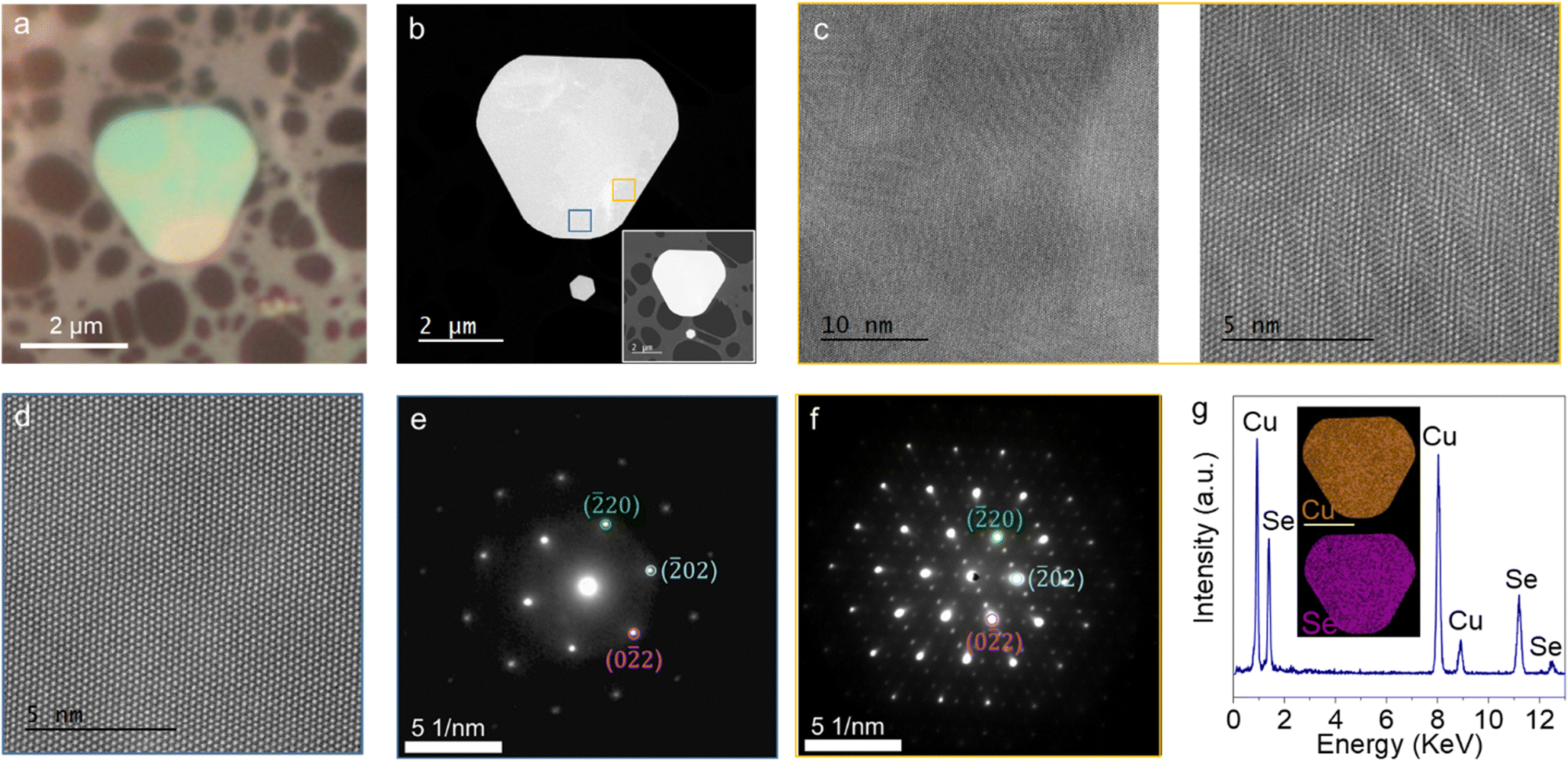 | ||
| Fig. 2 (a) Optical microscopy image of a Cu2Se crystal on a holey-carbon TEM grid. (b) HAADF-TEM image of a different sample is shown. The inset is a bright-field TEM image. Marked regions show where HAADF-STEM maps are collected. (c) HAADF-STEM images of regions that exhibit a moiré pattern (left panel), zoomed-in area (right panel), and (d) with no moiré pattern. (e) The SAED collected from the region without a moiré pattern matches well with the cubic crystal system along the [111] zone axis. Interplanar spacing of 2.05 Å is measured for the marked planes. (f) SAED from the region with a moiré pattern shows supercell reflections. Crystal planes are marked with the same zone axis, and 2.05 Å is measured for the marked planes as well. (g) EDX spectra and maps for Cu and Se in the inset are provided. The scale bar is 2 μm. | ||
We noticed that depending on the substrate type, confinement, and cooling rate from the synthesis temperature, Cu2Se crystals develop optically contrasting regions (Fig. 1c). When the crystal cooled down naturally from the growth temperature, a noticeable color contrast emerges at the corners of the crystals, particularly those grown on mica substrates. However, when the crystals cooled faster by promptly opening the furnace lid at approximately 670 K, the color-contrasting regions were dispersed randomly across the crystal (see Fig. S1, ESI†). The formation of the color-contrasting regions is directly linked to the Cu-deficient sites, as we shall demonstrate later. The mechanism leading to the Cu deficiencies and how they spread on the crystals might be attributed to the influence of the substrate and the cooling rate, which may affect the crystallographic orientation. The edges of the Cu2Se have a wedge-shaped facet formation (see Fig. S2 and S3, ESI†), and different crystallographic orientations may lead to different oxidation rates as reported for other materials.40 Further investigations are imperative to elucidate the exact mechanisms underlying the emergence of the contrasting regions. However, as we will discuss later, these regions play a crucial role in the observed phase transitions.
2.2. Optically contrasting regions of Cu2Se
Here, we will focus on the differences of optically contrasting regions of Cu2Se, below 414 K. Utilizing high-angle annular dark field scanning TEM (HAADF-STEM) and selected area electron diffraction (SAED), we examined flakes with apparent color contrast transferred to a holey carbon-supported Cu grid, similar to what is shown in Fig. 2a. It is challenging to find the exact location of the boundary between optically contrasting regions in TEM as there is no clear contrast under electron beam imaging (Fig. 2b). However, we noticed regions in HAADF-STEM scans with a distinct moiré pattern, different than other parts of the crystal (Fig. 2c and d). The SAED pattern from non-moiré regions (Fig. 2e) matches well with the cubic crystal structure of α-Cu2Se, which possesses the Fm![[3 with combining macron]](https://www.rsc.org/images/entities/char_0033_0304.gif) m space group. This can be attributed to an e-beam heating-induced phase transition as observed in other phase change materials.41 Further investigation is required to elucidate how electron beams affect different optically contrasting regions in Cu2Se via electron doping or e-beam-induced heating. The SAED patterns from the moiré regions (Fig. 2f) exhibit peculiar supercell reflections around the primary peaks corresponding to the Fmm space group in a cubic structure. This hints at Cu+ vacancy ordering as reported before.42,43 These vacancies form an ordered super-structure with a periodicity of 0.68 nm along the [111] crystallographic axis. A simulated SAED pattern is given in Fig. S4 (ESI†). The EDX survey given in Fig. 2g shows the presence of Cu and Se exclusively. The inset of Fig. 2g also demonstrates the elemental mapping where Cu and Se are uniformly distributed throughout the crystal regardless of the optical contrast differences within the flake. The findings indicate that the variations in Cu content are not significant enough to be observed in EDX maps.
m space group. This can be attributed to an e-beam heating-induced phase transition as observed in other phase change materials.41 Further investigation is required to elucidate how electron beams affect different optically contrasting regions in Cu2Se via electron doping or e-beam-induced heating. The SAED patterns from the moiré regions (Fig. 2f) exhibit peculiar supercell reflections around the primary peaks corresponding to the Fmm space group in a cubic structure. This hints at Cu+ vacancy ordering as reported before.42,43 These vacancies form an ordered super-structure with a periodicity of 0.68 nm along the [111] crystallographic axis. A simulated SAED pattern is given in Fig. S4 (ESI†). The EDX survey given in Fig. 2g shows the presence of Cu and Se exclusively. The inset of Fig. 2g also demonstrates the elemental mapping where Cu and Se are uniformly distributed throughout the crystal regardless of the optical contrast differences within the flake. The findings indicate that the variations in Cu content are not significant enough to be observed in EDX maps.
We imaged the edges of the crystals to formulate our hypothesis on the formation of the optical contrasting phase. SEM images of the crystal edges (Fig. S3, ESI†) along with the TEM analysis show that the {101} family of crystal planes are the dominant termination facet of the crystals. At this angle the tetrahedral sites reside on the surface of the facet, exposing it to the ambient atmosphere. Based on the HAADF-STEM, SAED, and SEM characterization of the samples, we hypothesize that some Cu+ reacts with the oxygen under ambient conditions through these facets, after the growth. The process continues until the diffusive motion of Cu ions from the bulk of the crystal is no longer sufficient to fill the edge sites. This leads to a Cu deficiency at the corners of the crystal. As a result, the Fermi level shifts into the valence band, and the corners become metallic. It is not possible to quantify the amount of deficiency in our samples, yet when there is enough Cu vacancy to induce the phase transition, all the excess Cu ions within the newly formed phase are expelled. This creates a phase boundary and uniform-looking domains at room temperature. The IMT outlined above also explains why these regions have different optical contrasts than the rest of the sample. This hypothesis can be tested by heating the crystals to increase the rate of Cu oxidation to induce more vacancies.
To verify the ion oxidation through the corners of the crystal, we heated the crystals under the ambient conditions to increase the ion oxidation rate. Newly created Cu ion vacancies should expand the area of dark contrasting regions (phase at the corners). This is exactly what we observed in samples heat cycled from room temperature to 388 K back to room temperature. We compared the ratio of dark contrasting regions (A) to the total area of the crystal (A0) before and after thermal cycling. A/A0 increases by more than twofold. Fig. 3a shows optical microscope images of a Cu2Se crystal during thermal cycling. When we repeat the thermal cycling under vacuum, we find the dark configuration area to be the same as the initial condition (Fig. 3b). During ambient heat cycling of the samples, as the temperature increases, the dark region expands from the corners. Optical images for other thermal cycled samples are given in Fig. S5 and S6 in the ESI.† We also would like to note that there is hysteresis between the areal ratio vs. temperature during heating and cooling. Upon cooling, the bright configuration emerges below ∼360 K. This entire observation can be explained by Cu ion vacancy migration and ordering. The room temperature phase separation due to Cu vacancies has been predicted previously by ab initio studies8,11,15 and the structures are derived from the β-phase by modifying the (001) plane of the pseudo-fcc sublattice of Se atoms in various configurations. Despite the small energy difference between the ordered configurations, long-range ordering-induced phase aggregation is possible9 and has been observed in ultra-small clusters43 of Cu2Se and hydrogen-doped VO2 nanobeams.34,44,45
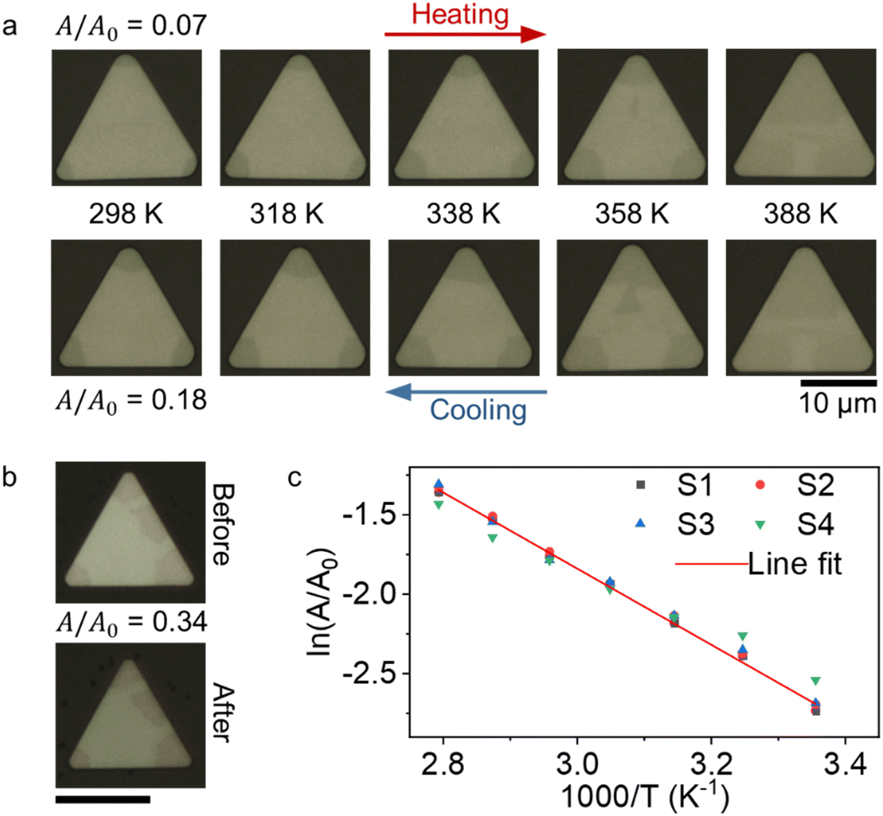 | ||
| Fig. 3 (a) Optical microscopy micrographs of a Cu2Se crystal taken during thermal cycling. After cooling down to room temperature, the A/A0 ratio increases more than two times. (b) When thermal cycling is performed under 10−2 mbar vacuum, no change is measurable in A/A0. The scale bar is 10 μm. (c) Arrhenius plot of A/A0versus T−1 for four different samples of similar size. The average activation energy is calculated from the slope of the lines fit to be EA = 0.207 ± 0.053 eV. | ||
The temperature-dependent expansion of the dark phase area can be measured to extract the energy barrier between the dark and the pristine phase. Fig. 3c shows the Arrhenius behavior of 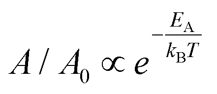 for four different samples, where T is the temperature at which A/A0 is calculated, EA is the activation energy and kB is the Boltzmann constant, with EA = 0.207 ± 0.053 eV. Error is defined from the line fitting. The measured activation energy is very close to the total energy difference between different phases of the β-phase reported in the literature.11,15 These observations and measurement of the activation energy between the dark and the pristine phase are consistent with the Cu ion-induced IMT picture hypothesized earlier.
2.3. Inelastic optical spectroscopy
We performed Raman and photoluminescence (PL) spectroscopy on our Cu2Se at room temperature as well as at elevated temperatures up to 454 K. A micro-Raman/PL setup equipped with a 532 nm laser beam that can be focused to a spot at the diffraction limit is used for the measurements. First, we compared the spectra of the dark and pristine regions at room temperature. We limited the laser power to 10 μW (∼60 kW cm−2) to avoid the formation of the dark phase optically, as demonstrated in the next section. The dark phase shows a broad PL peak centered around 2.1 eV (∼600 nm), while the pristine part of the crystal shows a single peak around 227 cm−1 (∼538.5 nm in the graph), which could be due to the Raman scattering, over an elevated featureless background (Fig. 4a). We attribute the enhanced signal to the hot PL,14,46 which is prominent in metals with d-orbitals. PL mapping also matches well with the dark phase distribution over the sample. The hot PL emerges from the direct recombination of holes in the d-band with the electrons in the conduction band below the Fermi energy. However, in the insulating phase, PL is not present as the energy gap is present due to correlation effects, and thermalization occurs via non-radiative channels.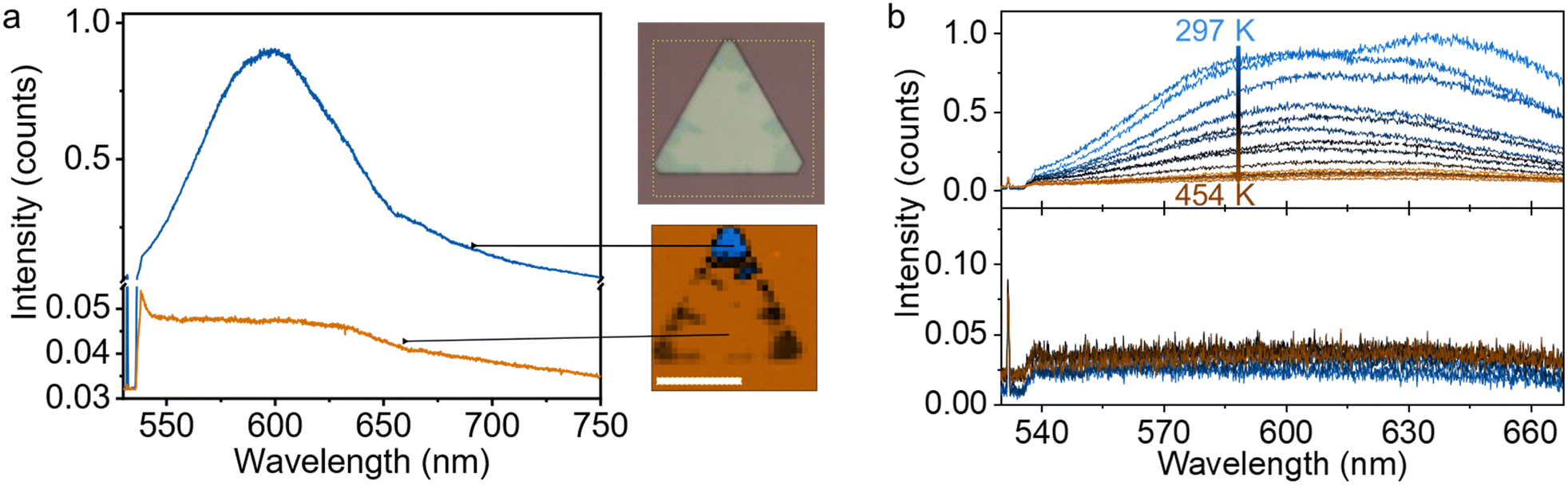 | ||
| Fig. 4 (a) Photoluminescence spectra of the dark and the bright configurations are shown. The panel on the right shows the optical microscopy image and the integrated PL intensity map around 600 nm of the dashed region. The scale bar is 10 μm. (b) Temperature-dependent PL spectra of the dark (upper graph) and the bright (lower graph) phases are given. The intensity counts are normalized to 1. | ||
Next, we performed temperature-dependent PL measurements from room temperature to 454 K (Fig. 4b), both from the pristine and dark phases. As elucidated in the previous part, increasing temperature plays two roles: (1) the mobility of Cu vacancies increases, and Cu vacancies diffuse into pristine regions of the crystal, and (2) the edge oxidation rate increases. As a result, more vacancies are formed, and these vacancies are more uniformly distributed over the entire sample at elevated temperatures. Since Cu ion vacancy per unit cell is less and Cu ions can also occupy different lattice sites, the PL intensity from the dark region decreases with increasing temperature. We would like to note that, in some samples, a secondary PL peak appeared around 1.9 eV (∼640 nm) (Fig. 4b). This can be attributed to a new phase with a different Cu deficiency, yet further experiments are required to elucidate the presence of the second PL peak.
2.4. Optical manipulation of the phase configuration
The phase configuration, i.e., distribution of phases over a crystal, can be manipulated using a focused laser beam even at low laser intensities (∼kW cm−2). We used this observation to perform controlled experiments to further support our hypothesis based on the IMT induced by copper deficiency. Fig. 5a and b show a series of optical microscopy micrographs of a crystal manipulated with a diffraction limited-focused laser spot (beam waist FWHM ≅ 500 nm), taken under the micro-PL microscope with the 532 nm high pass filter inserted. The dark phase is spatially moved even with a relatively low laser power (125 μW) and remains in the new position even after the laser is off. The fluid-like motion of the phase configuration shows the long-range ordering of the low-temperature configurations (see the Supporting Video, ESI†). It is also interesting to note that the dark phase edges have a hexagonal boundary (Fig. 5a-iii).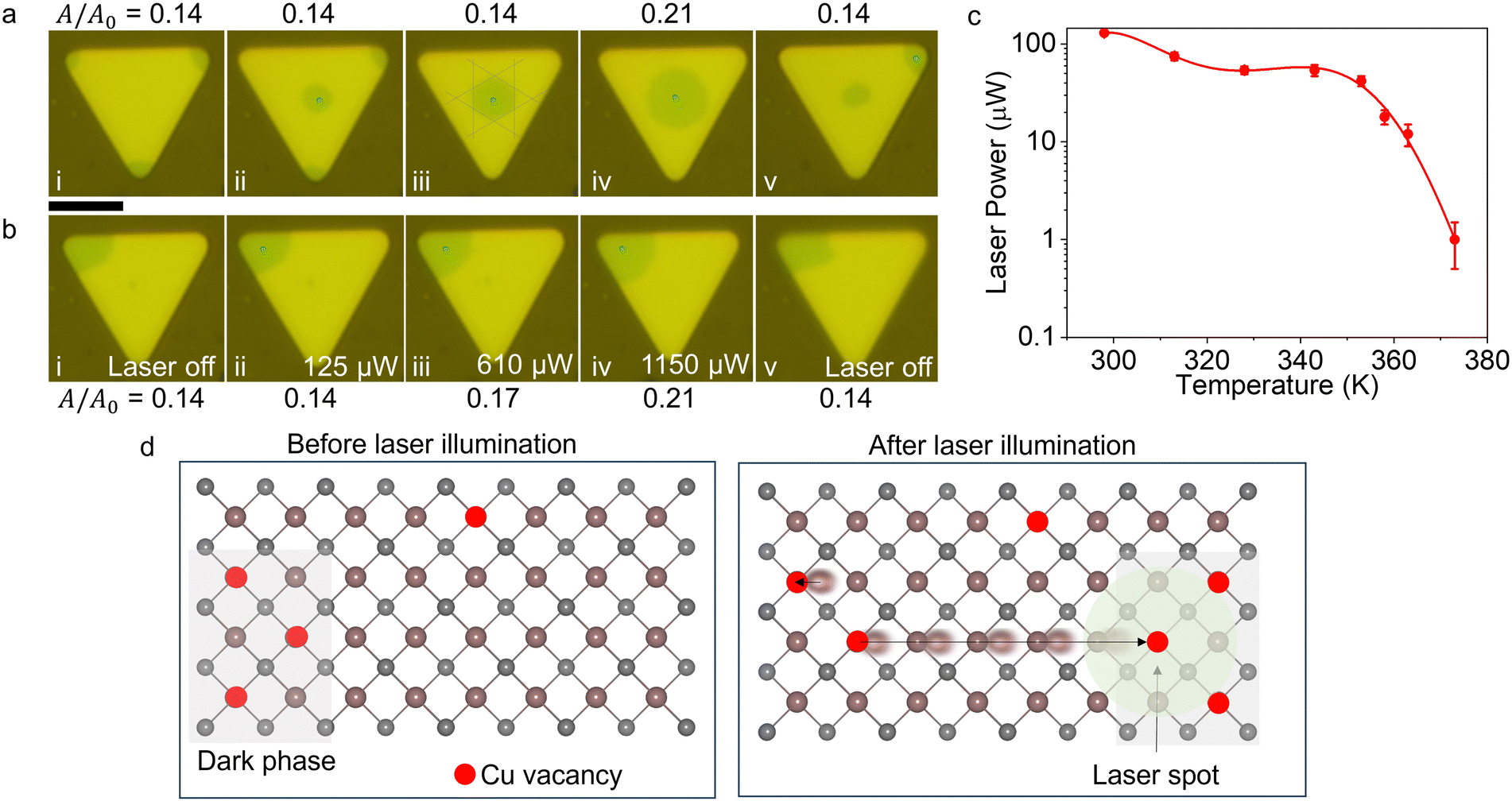 | ||
| Fig. 5 (a) A series of optical microscope images to show laser manipulation of spatial phase configurations. (i) Pristine crystal with the dark phase at the corners, (ii) a 532 nm laser beam (marked with the green dot) focused on a diffraction-limited spot on the center of the crystal with ∼100 μW power attracting the dark configuration to the center, and (iii) the dark configuration is completely pulled at the center. The dashed gray lines outline the hexagonal boundaries of the dark phase. (iv) The laser power is increased to ∼1 mW. The dark area expands to a point where a further increase in the laser power doesn’t change the A/A0 ratio (indicated above each image). The hexagonal outline is preserved. (v) Once the laser power is reduced and the laser is positioned at the corner of the crystal, some of the dark phase is moved to the corner. The scale bar is 5 μm. (b) The same crystal in (a) is shown. The dark phase is collected at the left upper corner of the crystal. The series of images from (i) to (iv) shows the effect of increasing laser power when the laser is placed over the dark phase. (i) From 0 μW to 125 μW, we observed no change in A/A0 ratio (indicated below each image). (ii)–(iv) The A/A0 ratio increases with the increasing laser power. Beyond 1150 μW, no change in A/A0 ratio is observed. (v) Once the laser beam is blocked, the A/A0 ratio shrinks to the pristine value. (c) Minimum laser power required to create the dark and the high-T dark configurations from the bright configuration. The solid line shows a polynomial fit to aid the eye. (d) A crystal schematic of Cu2Se, viewed from the [111] zone axis of the cubic phase for simplicity, showing a vacancy (marked by red circles) ordered dark phase on the left panel. On the right panel, laser-induced driving of Cu ions into vacancies is illustrated. | ||
One peculiar aspect of the laser-induced reconfiguration of the dark phase is that the ratio of the dark area to the total area (A/A0) of the crystal remains unchanged. The ratio for the crystal in Fig. 5a-i to -iii remains at 0.14 regardless of the reconfiguration. We observed this invariance at different temperatures as well (Fig. S7, ESI†). Once the laser power is increased even further (∼1 mW), the dark configuration expands to A/A0 = 0.21 (Fig. 5a-iv). Beyond 1 mW, the ratio remains constant and when the laser is turned off, the dark configuration area shrinks to its original size (Fig. 5a-v). Only after applying larger laser powers (above 100 μW) for tens of minutes to several hours, depending on the laser power on the sample, the dark area expands irreversibly. This shows that laser beam induced heating causes an increased oxidation rate of the Cu ions.
Next, we demonstrated the effect of laser power on A/A0. First, we collected all the dark contrasting regions to a corner using 100 μW total power on the sample (Fig. 5b). Then, by gradually increasing the laser power, we measured the total area of the dark region. As mentioned before, up to 125 μW, no change in the dark area size is observed. From 125 to 1150 μW, the dark area increased. Any increase in laser power beyond 1150 μW did not cause an increase in the dark phase area as in Fig. 5b-iv. When the laser beam is blocked, the dark area is reverted to its original size. Moreover, there is a temperature-dependent laser power threshold that induces dark configuration. Fig. 5c shows the change in the threshold laser power vs. temperature of the crystal. The decrease in the threshold laser power hints that the energy required to induce the dark configuration decreases with increasing temperature.
These observations show that the dark phase area is not determined by the temperature distribution created by the laser beam but rather by the local configuration altered by laser-induced heating, which mediates the vacancy-driven phase configuration in a long range. When the laser beam locally heats a region, Cu ions are excited to hop from site to site. Although the rest of the crystal (beyond the laser spot and its immediate vicinity) is still at ambient temperature, the pressure from the laser-heated region pushes the copper ions to the corners and converts the dark phase to the pristine phase by attracting vacancies under and in the vicinity of the laser spot. Once the new phase is nucleated, it is stable. Further increases in the laser power cause no change in the dark region size as there are no vacancies left to push Cu ions into. Fig. 5d depicts the vacancy movement-mediated phase reconfiguration. The observed persistent phase modulation, even after the laser is removed, is a unique feature of this ion-mediated phase transition.
2.5. Electrical properties of Cu2Se
To gain a better understanding of the complex interplay of ionic motion with the crystal lattice in Cu2Se, we fabricated two terminal devices of Cu2Se. Device fabrication steps and device details are given in the Methods section. When the devices are measured for the first time, typically, they exhibit very large resistance on the order of mega-Ohms with a non-Ohmic response (Fig. 6a). This is consistent with the semiconducting nature of pristine Cu2Se. When a bias above a certain threshold, typically around 1 V with a compliance of 1 mA, is applied, the resistance drops by almost 6 orders of magnitude (Fig. 6b). A similar resistance drop is also observed on samples that are illuminated by a laser beam focused on the samples (Fig. S8, ESI†). This dramatic change in the electrical conductance can be attributed to insulator–metal transition due to the migration of Cu ions into the contacts. Indeed, we demonstrated that further biasing of the crystal in the metallic state results in Cu ion accumulation at the Au contacts (Fig. S9, ESI†). Temperature-dependent resistance measurements, given in Fig. 6c, exhibit low resistivity and a positive temperature coefficient of resistance, which are consistent with the metallic nature of the Cu deficient Cu2Se, as reported previously for Cu2Se synthesized via other methods.18,47,48 | ||
| Fig. 6 (a) I–V curve before applying the formation voltage, 1 V with 1 mA compliance. (b) I–V curve of the same device after forming the device. (c) The resistance–temperature graph shows a positive temperature coefficient of resistance. (d) A series of optical micrographs were collected during the I–V cycling. Panel (i) shows the optical contrast of the crystal before the application of the formation voltage. (ii) Is after forming the device, and (iii) is when a reverse bias is applied. The ground terminal is marked on the first panel. The scale bar is 10 μm. | ||
Optical changes in the phase configuration are simultaneously monitored during the I–V measurements. Fig. 6d shows the optical micrographs of three major contrast changes observed optically in the device. Fig. 6d-i shows the device before applying large voltages. The phase configuration is affected by the device fabrication steps. Fig. 6d-ii show the phase configuration after applying 1 V. Fig. 6d-iii show another phase contrast distribution after the application of reverse bias. The motion of the dark contrasting region is consistent with the motion of Cu vacancies, as discussed in the previous section. The Supporting Video (ESI†) shows the real-time changes recorded under the optical microscope during I–V cycling. Fig. S10 (ESI†) illustrates our extended temperature-dependent resistivity measurements up to 408 K.
3. Conclusion
In conclusion, we demonstrated the synthesis of large-area ultra-thin Cu2Se crystals on sapphire and mica substrates. Our results show that copper vacancies created by the edge-oxidation of the Cu in single-crystalline β-Cu2Se result in an optically distinguishable insulator–metal transition that can be manipulated electrically and optically. Our results show that the dark, Cu-deficient phase has strong, broad photoluminescence that can be attributed to hot photoluminescence. The ability to control the vacancy order on the length scale of crystallite dimensions may enable novel applications in optical switching based on ion-mediated phase transition. These results show that Cu2Se can be a prototypical material for studying ion-mediated IMT and is promising for applications beyond thermoelectrics.2,20,49,504. Methods
Sapphire substrates were ultrasonically pre-cleaned in isopropanol and deionized water and dried using a high-purity N2 spray gun and the mica was freshly cleaved with a surgical blade with no additional cleaning process. The target substrate was placed downstream of the tube, and 10 mg of Se powder was placed in a crucible upstream. Then, CuCl powder (10 mg) was placed in a separate crucible in the center of the furnace, about 1 cm away from the substrate. The system was pumped down to 2.0 × 10⁻² mbar, then purged with Ar gas for five minutes and heated to the optimum growth temperature (923 K and 973 K for sapphire and mica, respectively). During growth, ambient pressure was maintained in the system, and the dwell time was set to 5 minutes. After growth, the system was cooled naturally to room temperature.Two terminal devices were fabricated through standard optical lithography procedures followed by thermal evaporation of 5 nm Cr followed by 100 nm Au.
Author contributions
A. A. S., A. P., and M. R. contributed equally to this work. A. A. S. synthesized the Cu2Se crystals. A. A. S. and A. P. worked on the synthesis and structural characterization. M. R. performed the device fabrication as well as the temperature-dependent electrical measurements. U. B. and D. P. contributed to the optical measurements. S. O, H. Y. J. and K. K. were involved with the TEM measurements. T. S. K. conceived the experiments and wrote the manuscript. All the authors commented on the writing of the manuscript.Conflicts of interest
There are no conflicts to declare.References
- J. B. Boyce and B. A. Huberman, Phys. Rep., 1979, 51, 189–265 CrossRef CAS.
- W. Di Liu, L. Yang and Z. G. Chen, Nano Today, 2020, 35, 100938 CrossRef.
- J. Y. Tak, W. H. Nam, C. Lee, S. Kim, Y. S. Lim, K. Ko, S. Lee, W. S. Seo, H. K. Cho, J. H. Shim and C. H. Park, Chem. Mater., 2018, 30, 3276–3284 CrossRef CAS.
- X. Cai, H. Jing, H. Wuliji and H. Zhu, J. Phys. Chem. C, 2023, 127, 5576–5583 CrossRef CAS.
- A. A. Sirusi, S. Ballikaya, C. Uher and J. H. Ross, J. Phys. Chem. C, 2015, 119, 20293–20298 CrossRef CAS.
- C. Zhou, Y. Yu, Y. K. Lee, O. Cojocaru-Mirédin, B. Yoo, S. P. Cho, J. Im, M. Wuttig, T. Hyeon and I. Chung, J. Am. Chem. Soc., 2018, 140, 15535–15545 CrossRef CAS PubMed.
- X. Zhao, S. Ning, N. Qi, Y. Li, Y. Dong, H. Zhang, J. Liu, B. Ye and Z. Chen, ACS Appl. Mater. Interfaces, 2021, 13, 58936–58948 CrossRef CAS PubMed.
- P. Lu, H. Liu, X. Yuan, F. Xu, X. Shi, K. Zhao, W. Qiu, W. Zhang and L. Chen, J. Mater. Chem. A, 2015, 3, 6901–6908 RSC.
- P. Lu, W. Qiu, Y. Wei, C. Zhu, X. Shi, L. Chena and F. Xu, Acta Crystallogr., Sect. B: Struct. Sci., Cryst. Eng. Mater., 2020, 76, 201–207 CrossRef CAS PubMed.
- A. Tonejc and A. M. Tonejc, J. Solid State Chem., 1981, 39, 259–261 CrossRef CAS.
- M. C. Nguyen, J. H. Choi, X. Zhao, C. Z. Wang, Z. Zhang and K. M. Ho, Phys. Rev. Lett., 2013, 111, 165502 CrossRef PubMed.
- H. Chi, H. Kim, J. C. Thomas, G. Shi, K. Sun, M. Abeykoon, E. S. Bozin, X. Shi, Q. Li, X. Shi, E. Kioupakis, A. Van Der Ven, M. Kaviany and C. Uher, Phys. Rev. B: Condens. Matter Mater. Phys., 2014, 89, 195209 CrossRef.
- O. Milat, Z. Vučić and B. Ruščić, Solid State Ionics, 1987, 23, 37–47 CrossRef CAS.
- A. Mooradian, Phys. Rev. Lett., 1969, 22, 185 CrossRef CAS.
- W. Qiu, P. Lu, X. Yuan, F. Xu, L. Wu, X. Ke, H. Liu, J. Yang, X. Shi, L. Chen, J. Yang and W. Zhang, J. Chem. Phys., 2016, 144, 194502 CrossRef PubMed.
- T. Takahashi, O. Yamamoto, F. Matsuyama and Y. Noda, J. Solid State Chem., 1976, 16, 35–39 CrossRef CAS.
- R. D. Heyding and R. M. Murray, Can. J. Chem., 1976, 54, 841–848 CrossRef CAS.
- Z. Vučić, O. Milat, V. Horvatić and Z. Ogorelec, Phys. Rev. B: Condens. Matter Mater. Phys., 1981, 24, 5398–5401 CrossRef.
- W. Borchert, Z. Kristallogr. - Cryst. Mater., 1954, 106, 5–24 CrossRef.
- H. Liu, X. Shi, F. Xu, L. Zhang, W. Zhang, L. Chen, Q. Li, C. Uher, T. Day and G. J. Snyder, Nat. Mater., 2012, 11, 422–425 CrossRef CAS PubMed.
- N. Frangis, C. Manolikas and S. Amelinckx, Phys. Status Solidi, 1991, 126, 9–22 CrossRef CAS.
- S. A. Danilkin, M. Avdeev, T. Sakuma, R. Macquart, C. D. Ling, M. Rusina and Z. Izaola, Ionics, 2011, 17, 75–80 CrossRef CAS.
- D. J. Voneshen, H. C. Walker, K. Refson and J. P. Goff, Phys. Rev. Lett., 2017, 118, 145901 CrossRef CAS PubMed.
- K. Yamamoto and S. Kashida, Solid State Ionics, 1991, 48, 241–248 CrossRef CAS.
- K. Yamamoto and S. Kashida, J. Solid State Chem., 1991, 93, 202–211 CrossRef CAS.
- A. N. Skomorokhov, D. M. Trots, M. Knapp, N. N. Bickulova and H. Fuess, J. Alloys Compd., 2006, 421, 64–71 CrossRef CAS.
- S. M. K. Nazrul Islam, P. Mayank, Y. Ouyang, J. Chen, A. K. Sagotra, M. Li, M. B. Cortie, R. Mole, C. Cazorla, D. Yu, X. Wang, R. A. Robinson and D. L. Cortie, Acta Mater., 2021, 215, 117026 CrossRef CAS.
- J. Heo, D. Dumett Torres, P. Banerjee and P. K. Jain, Nat. Commun., 2019, 10, 1505 CrossRef PubMed.
- L. Chen, J. Liu, C. Jiang, K. Zhao, H. Chen, X. Shi, L. Chen, C. Sun, S. Zhang, Y. Wang and Z. Zhang, Adv. Mater., 2019, 31, 1804919 CrossRef PubMed.
- M. Horvatic, I. Aviani and M. Ilic, Solid State Ionics, 1989, 34, 21–24 CrossRef CAS.
- M. Horvatić and Z. Vučić, Solid State Ionics, 1984, 13, 117–125 CrossRef.
- S. A. Danilkin, M. Avdeev, M. Sale and T. Sakuma, Solid State Ionics, 2012, 225, 190–193 CrossRef CAS.
- J. Wei, Z. Wang, W. Chen and D. H. Cobden, Nat. Nanotechnol., 2009, 4, 420–424 CrossRef CAS PubMed.
- T. S. Kasirga, D. Sun, J. H. Park, J. M. Coy, Z. Fei, X. Xu and D. H. Cobden, Nat. Nanotechnol., 2012, 7, 723–727 CrossRef CAS PubMed.
- J. H. Park, J. M. Coy, T. Serkan Kasirga, C. Huang, Z. Fei, S. Hunter and D. H. Cobden, Nature, 2013, 500, 431–434 CrossRef CAS PubMed.
- S. D. Kang, S. A. Danilkin, U. Aydemir, M. Avdeev, A. Studer and G. J. Snyder, New J. Phys., 2016, 18, 13024 CrossRef.
- H. Zhao, H. Hu, J.-W. Li, J.-F. Li and J. Zhu, Adv. Funct. Mater., 2023, 33, 2304663 CrossRef CAS.
- Y. Sun, L. Xi, J. Yang, L. Wu, X. Shi, L. Chen, J. Snyder, J. Yang and W. Zhang, J. Mater. Chem. A, 2017, 5, 5098–5105 RSC.
- W.-D. Liu, L. Yang, Z.-G. Chen and J. Zou, Adv. Mater., 2020, 32, 1905703 CrossRef CAS PubMed.
- Q. Zhu, Z. Pan, Z. Zhao, G. Cao, L. Luo, C. Ni, H. Wei, Z. Zhang, F. Sansoz and J. Wang, Nat. Commun., 2021, 12, 1–8 CrossRef PubMed.
- Y. Zhang, Y. Wang, Y. Wu, X. Shu, F. Zhang, H. Peng, S. Shen, N. Ogawa, J. Zhu and P. Yu, Nat. Commun., 2023, 14, 4012 CrossRef CAS PubMed.
- S. Kashida and J. Akai, J. Phys. C: Solid State Phys., 1988, 21, 5329–5336 CrossRef CAS.
- S. L. White, P. Banerjee and P. K. Jain, Nat. Commun., 2017, 8, 1–11 CrossRef PubMed.
- Y. Filinchuk, N. A. Tumanov, V. Ban, H. Ji, J. Wei, M. W. Swift, A. H. Nevidomskyy and D. Natelson, J. Am. Chem. Soc., 2014, 136, 8100–8109 CrossRef CAS PubMed.
- A. M. Chippindale, P. G. Dickens and A. V. Powell, J. Solid State Chem., 1991, 93, 526–533 CrossRef CAS.
- Y. Sivan and Y. Dubi, ACS Nano, 2021, 15, 8724–8732 CrossRef CAS PubMed.
- H. Liu, X. Yuan, P. Lu, X. Shi, F. Xu, Y. He, Y. Tang, S. Bai, W. Zhang, L. Chen, Y. Lin, L. Shi, H. Lin, X. Gao, X. Zhang, H. Chi, C. Uher, H. Liu, X. Yuan, P. Lu, X. Shi, F. Xu, Y. He, W. Zhang, L. Chen, Y. Tang, S. Bai, Y. Lin, L. Shi, H. Lin, X. Gao, X. Zhang, H. Chi and C. Uher, Adv. Mater., 2013, 25, 6607–6612 CrossRef CAS PubMed.
- D. Byeon, R. Sobota, K. Delime-Codrin, S. Choi, K. Hirata, M. Adachi, M. Kiyama, T. Matsuura, Y. Yamamoto, M. Matsunami and T. Takeuchi, Nat. Commun., 2019, 10, 1–7 CrossRef PubMed.
- L. Yang, J. Wei, Y. Qin, L. Wei, P. Song, M. Zhang, F. Yang and X. Wang, Mater, 2021, 14, 2075 CrossRef CAS PubMed.
- C. Xing, Y. Zhang, K. Xiao, X. Han, Y. Liu, B. Nan, M. G. Ramon, K. H. Lim, J. Li, J. Arbiol, B. Poudel, A. Nozariasbmarz, W. Li, M. Ibáñez and A. Cabot, ACS Nano, 2023, 17, 8442–8452 CrossRef CAS PubMed.
Footnotes |
| † Electronic supplementary information (ESI) available. See DOI: https://doi.org/10.1039/d4nh00003j |
| ‡ Equal contribution. |
| This journal is © The Royal Society of Chemistry 2024 |