
 Open Access Article
 This Open Access Article is licensed under a Creative Commons Attribution-Non Commercial 3.0 Unported Licence
Rational ligand design for enhanced carrier mobility in self-powered SWIR photodiodes based on colloidal InSb quantum dots†
Subhashri
Chatterjee
 ab,
Kazuhiro
Nemoto
a,
Hong-Tao
Sun
a and
Naoto
Shirahata
*abcd
ab,
Kazuhiro
Nemoto
a,
Hong-Tao
Sun
a and
Naoto
Shirahata
*abcd
aResearch Center for Materials Nanoarchitectonics (MANA), National Institute for Materials Science (NIMS), 1-2-1 Sengen, Tsukuba 305-0047, Japan
bGraduate School of Chemical Sciences and Engineering, Hokkaido University, Sapporo 060-0814, Japan
cDepartment of Physics, Chuo University, 1-13-27 Kasuga, Bunkyo, Tokyo 112-8551, Japan
dCNRS–Saint-Gobain–NIMS, IRL3629, Laboratory for Innovative Key Materials and Structures, National Institute for Materials Science, 1-1 Namiki, Tsukuba, Ibaraki 305-0044, Japan
First published on 19th March 2024
Abstract
Solution-processed colloidal III–V semiconductor quantum dot photodiodes (QPDs) have potential applications in short-wavelength infrared (SWIR) imaging due to their tunable spectral response range, possible multiple-exciton generation, operation at 0-V bias voltage and low-cost fabrication and are also expected to replace lead- and mercury-based counterparts that are hampered by reliance on restricted elements (RoHS). However, the use of III–V CQDs as photoactive layers in SWIR optoelectronic applications is still a challenge because of underdeveloped ligand engineering for improving the in-plane conductivity of the QD assembled films. Here, we report on ligand engineering of InSb CQDs to enhance the optical response performance of self-powered SWIR QPDs. Specifically, by replacing the conventional ligand (i.e., oleylamine) with sulfide, the interparticle distance between the CQDs was shortened from 5.0 ± 0.5 nm to 1.5 ± 0.5 nm, leading to improved carrier mobility for high photoresponse speed to SWIR light. Furthermore, the use of sulfide ligands resulted in a low dark current density (∼nA cm−2) with an improved EQE of 18.5%, suggesting their potential use in toxic-based infrared image sensors.
New conceptsThe ligand exchange step is often discussed as the reduction of inter-particle distance which influences the improved charge transfer in colloidal quantum dot-based photodiodes (QPDs). However, the reason behind improved carrier mobility and trap density has often not been studied or discussed. Interestingly, for InSb QPDs, there has been no exact study that reveals the science behind the improved figures of merit so far. Here, we have compared sulfide-capped treated InSb QPDs with previously reported bromide-capped InSb QPDs. The reduction of the interparticle distance was confirmed by HR-TEM with a wider area of the system; importantly, the inter-particle distance was approximately calculated by GI-XRD measurements. To understand the concept of close compactness of sulfide-capped QDs, we found from zeta potential that shortening the inter-particle distance of adjacent QDs, which is electronically neutral, is important. By performing SCLC calculations using more than 15 devices, we found that InSb CQDs with sulfide capping took precedence over those with bromine capping (i.e., the most common atomic capping ligand) in terms of better carrier mobility and low trap density. As expected, the sulfide-capped InSb QPD shows improved EQE and photoresponse speed. Additionally, this study achieves a dark current density in a similar range to that of commercial photodiodes by reducing the trap density of the QPD. |
1. Introduction
Short-wave infrared (SWIR) cameras and photodiodes are in high demand due to their photodetection capability in many critical futuristic applications, from night vision, emergent bio-imaging, food technology to remote sensing, light detection-ranging (LIDAR) and optical communication technologies.1–4 In recent imaging applications in the optoelectronics industry, high dark or leakage currents in photodiodes can trigger serious failures due to high external voltages or thermal noise.5 However, self-powered photodiodes do not require an external voltage source and can detect light with low power consumption.5–7 Most commercially available infrared detectors rely on epitaxially grown III–V and HgCdTe-based photodetectors, which require complex growth processes such as molecular beam epitaxy (MBE) and metal–organic chemical vapor deposition (MOCVD), resulting in high production costs and many manufacturing steps.8 Therefore, there is an urgent need to develop optical absorbers to easily fabricate SWIR photodetectors and improve device performance.Solution-processed colloidal quantum dot (CQD)-based photodetectors have received considerable attention due to their wavelength-specific sensing, high sensitivity and low-cost manufacturing processes9–13; furthermore, they can be integrated with readout integrated circuits (ROIC) and signal processing circuits at a lower cost. Until now, CQDs, which contain lead (Pb), cadmium (Cd), and mercury (Hg) as constituent elements, have been widely studied as photoactive materials for self-powered SWIR photodetectors,14–21 but the Restriction of Hazardous Substances Directive (RoHS) restricts these elements due to their high environmental toxicity.
To circumvent these toxicity issues, CQDs of III–V semiconductors and ternary CQDs such as indium arsenide (InAs), indium arsenide phosphide (InAs1−xPx) and indium antimonide (InSb) have attracted significant attention as alternative light absorbers for NIR to SWIR light sensing.22–28 InAs-based QPDs have achieved an external quantum efficiency (EQE) of ∼37% in the self-powered mode, mostly in the 950 nm NIR region. InAs1−xPx-based QPDs have been reported to show EQEs of 5%, 5% and 1% at SWIR wavelengths of 1140, 1270, and 1400 nm at −4 V of bias voltage, respectively. These papers motivated the development of QPDs using indium antimony (InSb) CQDs as optical absorption layers for SWIR light detection.
Bulk InSb, one of the direct bandgap semiconductors (0.17 eV at 300 K), has a large exciton Bohr radius (∼60 nm) and exhibits the highest room-temperature electron mobility (∼78![[thin space (1/6-em)]](https://www.rsc.org/images/entities/char_2009.gif) 000 cm2 V−1 s−1) and small exciton binding energy (0.5 meV) of any compound semiconductor.29 Colloidal synthesis routes for InSb CQDs have been developed over the past decade, but no significant progress has been made as photoactive layers for SWIR applications. Possible reasons could be defect-rich surface trapping the carriers, poor carrier mobility in the CQD film or low carrier dissociation probability.30 To address the drawback of low carrier mobility, in our previous work, we replaced the long molecular chain that is the terminal ligand of InSb CQDs with InBr3 molecules and demonstrated the first InSb-based SWIR QPD that can operate at 0 V,26 but encountered difficulties such as a high dark current density, a low external quantum efficiency and a slow response time in the second scale.
000 cm2 V−1 s−1) and small exciton binding energy (0.5 meV) of any compound semiconductor.29 Colloidal synthesis routes for InSb CQDs have been developed over the past decade, but no significant progress has been made as photoactive layers for SWIR applications. Possible reasons could be defect-rich surface trapping the carriers, poor carrier mobility in the CQD film or low carrier dissociation probability.30 To address the drawback of low carrier mobility, in our previous work, we replaced the long molecular chain that is the terminal ligand of InSb CQDs with InBr3 molecules and demonstrated the first InSb-based SWIR QPD that can operate at 0 V,26 but encountered difficulties such as a high dark current density, a low external quantum efficiency and a slow response time in the second scale.
Herein, we report the effect of a sulfide-capping ligand on the interparticle distance between adjacent InSb CQDs, dramatically improving the carrier mobility of the optically active layer compared to capping with bromide, a common atomic ligand. The sulfide-capped InSb-based QPDs successfully convert optical signals to electrical signals with self-powered photodiode characteristics even with 0 V attributes, along with a low dark current (∼10−9 A), which further implies its advantages for future applications.
2. Results and discussion
We started the synthesis by considering the concentration of super hydride (SH) as a reducing agent and the molecular ratio of the In/Sb precursors to suppress the oxidation of the resulting CQDs during the synthesis and formation of metallic antimony, which is difficult to solve.26,30–32 The optimized volume ratio of oleylamine (OLA) as a solvent with SH was 5.2 (see the Experimental section, ESI†). Scheme S1 (see ESI†) illustrates a size separation procedure that involves four-step centrifugation to narrow the size distribution of the CQDs. The samples obtained in each step were labelled as A, B, C and D.2.1. Characterization of OLA-capped InSb QDs
We performed several experiments to confirm the synthesis of highly crystalline, non-oxidized colloidal InSb QDs. Analysis of the powder X-ray diffraction (XRD) patterns shown in Fig. 1a confirms that samples A–D are pure-phase zinc flint structures without any secondary phases. The diffraction peaks centered at 2θ = 23.8°, 39.3° and 46.3° are characteristic of the (111), (220) and (311) planes, respectively. The broad peak at 21.52° can be attributed to the excess amount of organics remaining in sample D.33 The diffraction peaks broadened with the incremental addition of methanol as an antisolvent in the centrifugation process, suggesting a decrease in the average diameter of the QDs. Fig. 1b and c show representative X-ray photoelectron spectroscopic (XPS) spectra corresponding to the core levels of In 3d and Sb 3d, respectively. Panel (b) shows the chemical bonding state in which In is bound to Sb and not to oxygen, which is consistent with the literature.26 In panel (c), the overlapped XPS spectra of Sb 3d and O 1s core levels were deconvoluted as dotted lines. Sb 3d5/2 and Sb 3d3/2 peaks were assigned to In–Sb bonds at binding energies of 528.2 eV and 537.6 eV.34,35 Besides, the absence of a peak at 540.4 eV indicates that there is no Sb–O component. Inductively coupled plasma mass spectrometry (ICP-OES) study confirmed an In:Sb ratio of 1:1. These structural analyses indicated that the stoichiometric InSb QDs with a high degree of crystallinity and no surface oxidation were synthesized as the SH concentration in the feed solution was increased.
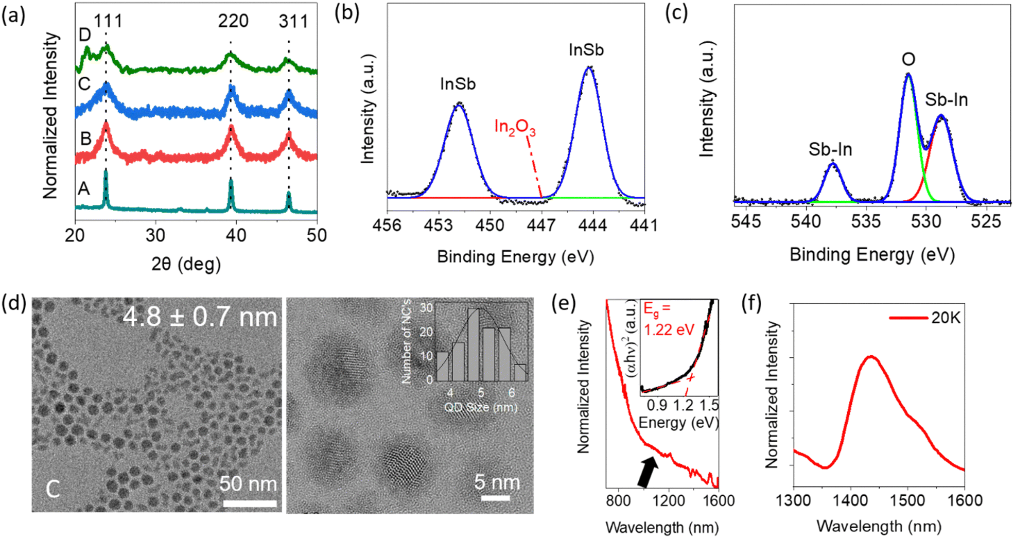 | ||
| Fig. 1 (a) Powder XRD patterns of the products prepared with different centrifugation processes; a detailed scheme has been added in Scheme S1 (see ESI†). XPS spectra in (b) In 3d and (c) Sb 3d core levels of sample C, fitted with a Gaussian function. (d) HR-TEM image of sample C with the size distribution profile shown in the inset. (e) Room-temperature NIR absorption spectrum of sample C dispersed in TCE. (f) PL spectra of sample C at a temperature of 20 K. | ||
HR-TEM images of samples A, B, C and D are shown in Fig. S2, S1d, S1d and S1a (see ESI†), respectively. In all samples, spherical QDs were isolated and dispersed without aggregation, suggesting that their surfaces were terminated with OLA molecules. The estimated diameters were 17 ± 2.9 nm, 8.7 ± 1.2 nm, 4.8 ± 0.7 nm and 2.6 ± 0.4 nm for samples A, B, C and D, respectively. The centrifugation process with stepwise addition of methanol allowed fractionation of the mother sample into a relatively narrow polydispersity (standard deviation, σ = ∼25–27%) sub-ensemble.
2.2. Optical properties of OLA-capped InSb QDs
THe optical properties were investigated to understand the relationship between the QD size and optical bandgap. The NIR absorption spectrum of sample C is presented in Fig. 1e while the spectra for samples B and D are shown in Fig. S1b and e (see ESI†). In these spectra, the excitonic peak energy positions are not clear but humps can be seen as shoulders at around 845 nm, 1100 nm and 1450 nm for samples B, C and D, respectively. This is probably due to the semi-ensemble size polydispersity of InSb QDs in the σ = 25–27% range, consistent with the literature.36 As will be discussed later in this paragraph, the hump shape becomes more obscured as a shoulder in the region of smaller QD size. On the other hand, no characteristic peak was observed in sample A, even though the diameter of the QDs was considerably smaller than the Bohr radius of the bulk exciton. Indeed, the appearance of the first excitonic peak in the absorbance spectrum is limited in the literature to cases where the diameter of the QD is smaller than 7 nm.30,36,37 It is plausible that the observed absence of an excitonic peak may be attributed to the broader size distribution of the CQDs, resulting in a weakened quantum confinement effect compared to smaller CQDs. (Fig. S2, see ESI†). The Tauc plots from which the optical bandgap energy can be determined are shown in the insets of Fig. 1e and Fig. S1b and e (see ESI†) for each sample. The estimated values were 0.86 eV, 1.22 eV and 1.60 eV for the 8.7-nm, 4.8-nm and 2.6-nm diameter QDs, respectively. To facilitate a quantitative comparison of size-dependent bandgaps, our experimental data were plotted along with the reported values and theoretical relationship calculated by the effective mass approximation (EMA, see Fig. S3, ESI†).38 The calculated EMA model indicates that the bandgap increases slowly in the range of QD diameters larger than 6 nm but increases rapidly in the range of QD diameters smaller than 5 nm. For d < 5 nm, even relatively small size deviations can cause a large shift in the photon energy of the exciton absorption, yielding spectral broadening. In other words, the standard deviation of σ = 25–27% is too large to generate the distinct exciton peaks in the absorption spectra for samples C and D. Conversely, for QDs larger than 8 nm in diameter (i.e., sample B), the band gap variation with QD size is small. Thus, the standard deviation of σ = 25–27% is small enough to produce a distinctly shaped hump, implying exciton absorption. The bandgap calculated with EMA showed an overestimated trend compared to bandgap attributed to the experimental values in the 2–6 nm size regime. Similar trends with InSb CQDs have been reported before.36,37 The possible mechanisms are the underestimated leakage of the wave functions into the adjacent media or beyond the band structure Γ and the dependency of 1/R on the Coulomb interaction, which has been ignored during the EMA calculation.36,37,39,40The photoluminescence (PL) spectra of samples B, C and D are shown in Fig. S1c, f and f (see ESI†), respectively. As expected from the prediction of EMA, the PL spectral peak position was varied from 1015 nm to 1445 nm by tuning the diameter of QDs from 2.6 ± 0.4 nm to 4.8 ± 0.7 nm. Such a large Stokes shift between the excitonic absorption and PL peak is commonly observed for InSb QDs and is attributed to the presence of internal defect states or polydispersity of CQDs in the system.41 The PL spectra of samples B and C were observed at room temperature, but the spectral intensity became weak for smaller QDs. Although the limited wavelength range of the SWIR detector did not allow us to detect the exact PL peak in sample B, it is particularly noteworthy that the 8.7-nm QDs showed the potential to be emitters with PL peaks at wavelengths longer than 1600 nm for the first time (see Fig. S1f, ESI†).
2.3. Ligand exchange of OLA with sulfide ions
In a typical synthesis, long-chain organic acids or bases attached to the CQD surface as ligands aid the homogeneous growth of nanocrystals and stabilize the CQDs in organic solvents.42,43 However, such ligands probably hinder the long-range charge carrier transport in CQD assemblies, yielding the reduced device performance of QPDs.44 For device design and development of QPDs, the exchange of long ligands allows the widespread choice of materials to improve performance, where charge carrier transport/transfer plays a major role.45 It is expected that the in-plane carrier mobility of the light-absorbing layer can be improved by shortening the interparticle distance in CQD assemblies, leading to improved device performance such as responsivity, EQE and photoresponse time. In this work, Na2S was exchanged with OLA ligands immobilized on InSb CQDs. The inorganic chalcogenide small-ligand sulfide was chosen because of its longer stability and low ionization energy donor for III–V semiconductors.46 Details of ligand engineering are explained in the Experiment section (see ESI†).During the synthesis of the InSb CQDs, OLA ligands were attached to the cation (In3+) as an L-type ligand.47 Ligand exchange can be described as a nucleophilic substitution at the metal site, while in the polar solvent, anions have lower solubility than cations. To exchange the OLA ligands with sulfide ones, a standard two-phase transfer protocol was performed. Briefly, in the post-synthesis step, the OLA-capped InSb CQDs dissolved in n-octane were vigorously mixed with a formamide (FA) solution of Na2S. As the reaction occurs over a few minutes, CQDs were completely transferred from the n-octane phase (top layer) to the FA phase (bottom layer), as shown in Fig. 2a and b, where chalcogenide ligands are favoured for electrostatical stabilization.48
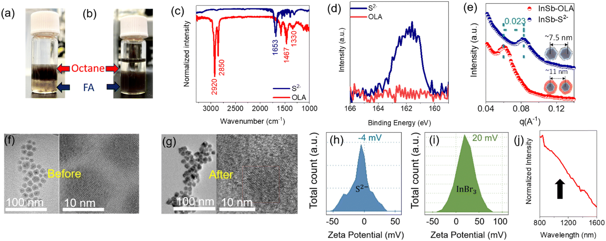 | ||
| Fig. 2 Photographs of phase change (a) before and (b) after sulfide ligand exchange. (c) ATR-FTIR spectra of the OLA-capped InSb CQDs before and after sulfide ligand exchange. (d) XPS S 2p spectra of OLA-capped CQD before and after sulfide ligand exchange. (e) Low-angle GIXRD spectra of InSb CQDs with OLA- and sulfide-capped ligands. HR-TEM images of (f) OLA- and (g) sulfide-capped InSb CQDs. Zeta potentials of InSb CQDs (approx. 2–3 mg ml−1 in DMF) capped with (h) sulfide and (i) bromide ligands. (j) Optical absorption spectrum of sulfide-capped InSb CQDs in the thin-film form. | ||
Next, the changes in the surface chemical properties of CQDs before and after Na2S treatment were characterized using attenuated total reflection Fourier transform infrared (ATR-FTIR) spectroscopy and XPS. Fig. 2c shows the ATR-FTIR spectra of the OLA-capped InSb CQDs, which demonstrate strong absorption bands in the aliphatic C–H stretching region between 2850 and 2960 cm−1 and the C–H bending/scissoring region between 1350 and 1500 cm−1.49 The C–H signatures disappeared after treatment with Na2S, whereas a single peak was observed at 1653 cm−1, which is attributed to the DMF complex.50 The XPS spectrum of the S 2p core level after Na2S treatment demonstrates the appearance of the peak cantered at 161 eV, indicating the formation of sulfide-capped CQDs by ligand exchange (Fig. 2d).51 Due to air exposure of the sample during transfer to the XPS instrument, a sulfate peak appeared at a binding energy of 168.8 eV (see Fig. S4a, ESI†). The cationic complex Na+ could not be washed out, the XPS peak showed a binding energy of 1070.6 eV (see Fig. S4b, ESI†). Additionally, the possible bonding of disulfide was analysed by XPS and Raman spectroscopy. Based on the previous literature, the presence of disulfide bonds can be substantiated by the XPS peak at a binding energy of 164 eV and Raman spectra peak in the wavenumber (cm−1) range of 520 to 530. Although the formation of disulfide bonds is facile when sulfide is used as a capping agent, we were unable to detect the presence of disulfide in the Raman spectra (see Fig. S4c, ESI†) and XPS spectra (see Fig. 2d). However, as shown in Fig. S4c, the peak appearing at 188 cm−1 was assigned to the InSb CQD.26
To elucidate the effect of sulfide termination on the interparticle distance of the CQDs in the photoactive layer, we measured the grazing-incidence small-angle X-ray diffraction (GI-XRD) patterns of the OLA-, sulfide- and bromide-capped InSb CQDs (see Fig. 2e and Fig. S5, ESI†), respectively. Halides, a well-known atomic ligand family, have been widely used to terminate the surface of CQDs for enhancing the charge carrier transport in CQD solids,14,26,52 and bromide served as a standard in this work. For accuracy of comparison, we used the same sample consisting of OLA-capped CQDs with a mean diameter of 5.5 ± 0.5 nm. The diffraction peak of the OLA-capped QDs occurred at 2θ = 0.85°, whereas the diffraction peaks were shifted to 2θ = 0.98° and 1.2° for the bromide- and sulfide-capped counterparts, respectively (see Fig. S5, ESI†). The estimated value of the interparticle distance of CQDs (edge-to-edge of CQDs) was reduced from 5.0 ± 0.5 nm (for OLA capping) to 1.5 ± 0.5 nm (for sulfide capping). It is worth noting that the interparticle distance of the sulfide-capped QD solid was significantly shorter than that of the bromide-capped counterpart (2.6 ± 0.3 nm). Furthermore, for the sulfide-capped CQD solid, the peak broadened as the peak-to-valley ratio decreased, suggesting an increase in the packing density of the CQDs.23 Transmission electron microscopy (TEM) revealed a reduction of the interdot distance, which indicates the successful exchange of ligands of InSb CQDs, while the sizes of the nanocrystals are unchanged after ligand exchange. HR-TEM images of several reports on sulfide-capped QDs form close vicinity with neighbours after ligand exchange, although the inter-dot distances are hardly mentioned and discussed.30,51,53–57 In this report, the decrease in interparticle distance was confirmed by HR-TEM observation, as shown in Fig. 2f and g, and shows a similar trend to that reported previously. Additional TEM images before and after ligand exchange are shown in Fig. S6 (see ESI†) for the samples. In the sample before treatment with Na2S, the CQDs were dispersed and isolated from each other, keeping the interparticle distance constant, as expected. In contrast, the CQDs aggregated in the sample after the OLA was exchanged with the sulfide ligand. This is an unexpected and interesting observation. Because the termination of CQDs with bromide (a typical atomic ligand) does not allow agglomeration, and the interparticle distance is kept constant.26 To quantitatively understand the difference in the CQD interaction between bromide and sulfide ligands, we measured the zeta potential of both samples of QDs highly dispersed in DMF. As shown in Fig. 2h, the sulfide-capped InSb CQDs in DMF solution showed a −4 mV of zeta-potential, which is nearly equal to electrically neutral. On the other hand, the zeta potential value of the bromide-capped InSb CQDs in DMF solution was +20 mV, as shown in Fig. 2i. Such a large difference in the zeta potential suggests that the steric repulsion on the CQD surface for sulfide-capped InSb CQDs is much weaker than that of bromide-capped counterpart, resulting in a difference in the dispersion behaviours of CQD solids observed by HR-TEM and GI-XRD.
Fig. 2j and Fig. S7 (see ESI†) shows the NIR absorption spectrum of a sulfide-capped CQD solid in the film and solution forms in DMF, respectively. A broad, clear excitonic characteristic was observed at around 1100 nm. We confirmed that the relationship between the bandgap and size was retained. A possible reason for the broad peak may be the agglomeration of the CQDs.
2.4. Fabrication of self-powered QDPs for SWIR sensing
DMF ink of the sulfide-capped InSb CQDs was used to fabricate SWIR photodiodes. Sample C was chosen as the photoactive material. The resultant InSb-QPD was compared with its bromide-capped counterpart to explore the effect of the shortened interparticle distance on device performance. An ultraviolet photoelectron spectroscopy (UPS) spectrum of the spin-coated sulfide-capped InSb CQD film, shown in Fig. 3a, demonstrates the low and high binding-energy cutoff regions, which were 0.82 eV and 16.6 eV, respectively. The work function was calculated from the difference in energy between the secondary electron cutoff and the excitation photon energy (hν = 21.22 eV), and the highest occupied molecular orbital (HOMO) value was estimated to be 5.44 eV. Using the magnitude of the bandgap of sample C (Eg = 1.22 eV), the lowest unoccupied molecular orbital (LUMO) value was estimated to be 4.22 eV. The Fermi energy level was estimated to be 4.62 eV. The proposed energy level diagram under zero applied bias is depicted in Fig. 3b. The HOMO and LUMO values of the PEDOT:PSS and ZnO films were obtained from the values reported in a previous paper.26 A typical cross-sectional scanning electron microscopy (SEM) image and EDS mapping, shown in Fig. 3c and Fig. S8 (see ESI†), demonstrate 20-nm thick ZnO and 10-nm thick PEDOT:PSS layers. The sulfide-capped InSb CQD layer had a thickness of 130 nm, and its surface was rough at the nanoscale because it started to aggregate in DMF. The photoactive area of the QPD was approximately 0.04 cm2. | ||
| Fig. 3 (a) UPS spectra of sulfide-capped InSb CQDs with high- and low-binding energy cutoff regions. (b) Energy band diagram of the QPD under no-bias condition. (c) Typical cross-sectional SEM image of the QPD stack. (d) I–V characteristics of the QPD in a linear form under different SWIR wavelengths of light; the inset shows the photoresponse of the QPD under different wavelengths of SWIR light. (e) and (f) EQE of the QPD and (g) and (h) responsivity of the QPD at 0 and −1 V, respectively. | ||
The device performances of the QPDs, where sulfide-capped InSb QDs served as photoactive layers, measured at room temperature in ambient air, are summarized in Fig. 3d–h and 4. The representative photocurrent–voltage characteristics (I–V) shown in Fig. 3d were obtained using sample C and measured under dark conditions (no illumination) and light illumination at different wavelengths ranging between 1000 nm and 1500 nm, while the photon power density of the incident light was fixed at 1 mW cm−2. The photocurrent generated was greater than the dark current, indicating that the device responded to light and was also dependent on the wavelength of the incident light. The highest photocurrent was achieved under 1100 nm wavelength light. The device responsivity and EQE are the figures of merit for photodiode devices. The photoresponsivity (R) is defined as in eqn (1):58
| R = (Ilight − Idark)/PinA | (1) |
| EQE = hcR/eλ | (2) |
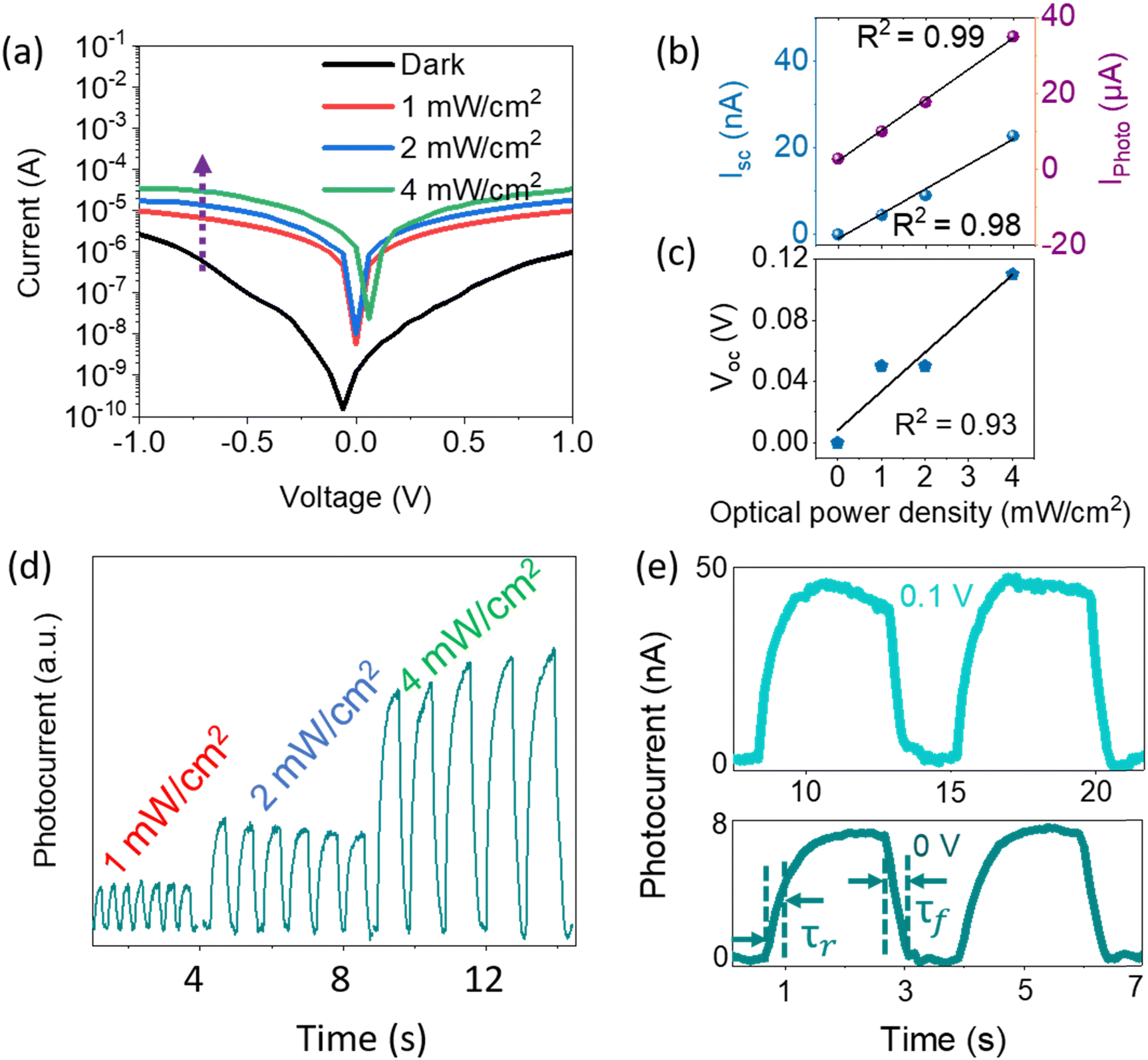 | ||
| Fig. 4 (a) Logarithmic I–V characteristics of the QPD at 1100 nm with different optical light intensities. Optical illumination intensity-dependent (b) Isc, Iphoto (−1 V) and (c) Voc values (linear fit) of the QPD. (d) Photoresponse of the QPD at different light intensities of 1100 nm light. (e) Photoresponse of the QPD at 0 and 0.1 V. | ||
Fig. 3e and g show the values of EQE and R at 0 V, respectively, which proves the self-powered operation of the QPD. The highest values of EQE and R for the QPD operated at 0 V with 1100-nm light at a power density of 1 mW cm−2 were 1.32% and 0.012 A W−1, respectively. As expected, the EQE and R of the photodiode were enhanced when a bias voltage was applied to the device, as shown in Fig. 3f and h. Similar enhancements were observed for the other incident light wavelengths. The best values of EQE and R under 1100 nm at −1 V were 18.52% and 0.18 A W−1, as presented in Table S1 (see ESI†).
Fig. 4a shows the I–V characteristics of the InSb-QPD on a logarithmic scale when the incident light optical power density at 1100 nm was varied between 1.0 and 4.0 mW cm−2. It was particularly noted that the dark current densities were as low as 3.8 nA cm−2 and 70 μA cm−2 at 0 V and −1 V, respectively, which were 3.5- and 3.15 times lower than those of the bromide-capped InSb QPD device, leading to enhanced EQE and responsivity. Further, the dark current density of the InSb QPD was also compared with InGaAs commercial Hamamatsu Photonics photodiodes, where our devices show a similar range (∼nA cm−2) of the dark current density with commercial one even at room temperature (RT).60 The current device also shows a lower dark current compared to the recent solution-processed QPD reports.27,61
Recently, it has been discussed that the dark current density of QPD devices is sensitive to both the trap density and the impurity levels within the energy bandgap and trap density of the host material.23 That is, a lower trap density and impurity energy level work as structural parameters that cause a lower dark current and a higher EQE. In this study, the UPS measurement of sulfide-capped CQDs showed 0.06 eV intrinsic behaviour compared to bromide-capped counterparts, which is one of the possible reasons for the decrease in the dark current (see Fig. S9, ESI†). Therefore, InSb QPDs have lower dark currents due to the lower doping, resulting in a lower trap density.
The photocurrent density was dependent on the optical power density of the incident light. With increasing optical power density, the photocurrent density increases up to 850 μA cm−2 at 4 mW cm−2. Fig. 4b displays the short-circuit current and photocurrent at −1 V, whereas the Voc of the QPD at different light intensities are shown in Fig. 4c. It shows a linear increase, which further implies the general work function of a photodiode; the R2 values are shown in the figures. Fig. 4d shows the enhanced intensity of the photoresponse with increasing optical power density of the incident light. A typical result of the time–response curves is shown in Fig. 4e, where a quick and reproducible photocurrent response and good cycling stability are observed at bias voltages of 0 V and 0.1 V. Furthermore, the response profile shows that the measured rise time (τr: from 10% to 90% of the saturated value) and fall time (τf: from 90% to 10% of the saturated value) are ∼200 msec and ∼200 msec at a bias voltage of 0 V. These values were 2.75 and 4.5 times lower than those of bromide-capped InSb CQD-based QPD.26 Such improvement was also observed under white light irradiation even at a very high optical power density (80 mW cm−2), especially in the fall time of the QPD (see Fig. S10, ESI†). Despite conducting measurements encompassing the photoresponse and I–V characteristics of the devices under ambient atmospheric conditions at room temperature and subjecting several devices to prolonged exposure to ambient atmosphere for a duration ranging from 30 to 45 days, it was noteworthy to observe that, even after prolonged exposure to air, the devices retained their photoresponse speed (see S11, ESI†). Specific detectivity (D*) was calculated by assuming shot noise as a primary contributor to the noise of the photodiode, as InSb is a low bandgap material.62 The D* of Na2S-treated InSb QPDs was 4 × 10¹⁰ Jones (Jones = cm Hz1/2 W−1) at −1 V under a wavelength of 1100 nm (see Fig. S12, ESI,† light intensity = 1 mW cm−2).
There are two possible reasons why device performance was improved by replacing the OLA ligand with a sulfide ligand. First, the in-plane carrier mobility of QD solids is enhanced by using sulfide-capped CQDs. As evidence, we prepared multiple hole-only devices and electron-only devices with both the ligands, as shown in Fig. S13 (see ESI†) and the best values shown in Fig. S14 (see ESI†), to estimate the carrier mobility and carrier trap density. The devices with bromide-capped InSb CQDs were used as standards. The trap-filled limit voltage (VTFL) shows almost consistent values when repeated in multiple devices, as summarized in Table S1 (see ESI†), while the error bar is plotted in Fig. S15 (see ESI†). The estimated carrier mobility and trap density from the space-charged limited current (SCLC) and trap-filled regimes are summarized in Table 1. This quantitative analysis showed that capping with sulfide ligands improved carrier mobility by a factor of 1.6 for electrons and 1.8 for holes. Furthermore, the sulfide-ligand reduced the carrier trap density by a factor of 1.57 for electrons and 1.47 for holes. In addition to the reduction of carrier traps, the improved carrier mobility between the QDs, especially due to the sulfide ligands, contributed to the improved device performance. Second, the HOMO–LUMO level of the sulfide-capped InSb CQDs shifted to higher energy values, resulting in a favourable energy band for better charge transport. The HOMO value of the sulfide-capped InSb CQD layer shifted to 5.44. This eventually decreases the energy barrier between the valence band maximum (VBM) of the photoactive layer and the VBM of the HTL layer PEDOT:PSS, which may increase the built-in potential (Vbi), enable better hole transportation, and improve the Voc.63,64 Thus, by improving the electron blocking with better hole extraction,65 the dark current is suppressed, resulting in a faster photoresponse. The 3-dB bandwidth of the photodiode was calculated using the photoresponse speed derived from the equation governing the bandwidth (BW) relation = 0.35/tr, where tr is the rise time of the photodiode.66 The BW of the sulfide-capped QPD was 63 Hz, whereas the BW of the bromide-capped QPD was 20 Hz. Compared to recent InSb QPDs, our devices exhibit a slower photoresponse speed,61,67 but demonstrate an improved EQE at −1 V, exceeding recent reports at 1100 nm with a very low current density (Table S1, see ESI†). Despite the advancements in surface oxidation mitigation and protective shell applications over InSb CQDs, the comprehensive enhancement of all relevant figures of merit remains elusive, highlighting the complex underlying mechanisms. Significant room for refinement in InSb QPDs persists, particularly in enhancing the photoresponse speed, EQE, and other metrics. We propose achieving this by formulating selective ligand engineering, adopting core–shell, CQD size-dependent QPD performance with mono distribution, exploring modifications in the device structure, and fabricating refined film formation by using a polypropylene filter (ppf) to narrow down the size distribution, eliminate agglomerated CQDs and study temperature-dependent I–V characteristics to comprehend interfacial defects, particularly aimed at mitigating the dark current under short-circuit and bias conditions.
| Ligand | E-only device μe (cm2 V−1 s−1) | H-only device μh (cm2 V−1 s−1) | Electron-only Nt (carrier number per cm3) | Hole-only Nt (carrier number per cm3) |
|---|---|---|---|---|
| Bromide | 0.012 | 0.01 | 9.3 × 10¹¹ | 1 × 10¹² |
| Sulfide | 0.02 | 0.018 | 5.9 × 10¹¹ | 6.8 × 10¹¹ |
3. Conclusions
We have modified the synthesised route to achieve pure InSb CQDs with easily available bromide precursors, which eventually caused no surface oxidation on the QD surface. Additionally, the size-selective precipitation procedure helped to achieve a narrower size distribution. Optical properties and bandgap were varied from 840 nm to 1450 nm at 1.6 eV to 0.86 eV, while photoluminescence was achieved from 1015 nm and 1440 nm for QD sizes of 2.6 nm and 4.8 nm, respectively. Post-synthesis ligand engineering with sulfide ligands was performed to improve the mobility and trap density of the QD surface, which eventually improved charge transfer between adjacent CQDs. Owing to a lower trap density, the sulfide-capped InSb QPD film achieves a very low dark current (∼ 3.8 nA cm−2), which is very competitive among commercial- and solution-processed SWIR photodiodes. Further, sulfide-capped InSb thin films show very high carrier mobility, which could be applicable vastly for SWIR fast sensing in the future. Further, fabricated sulfide-capped InSb QPDs responded to 5.5 ms in an ambient atmosphere as a self-powered photodiode and achieved an EQE of 18.5% at 1100 nm. The fast response with a promising figure of merit shows the potential to substitute Pb-, Hg- and As-free quantum dots for SWIR sensing. Further improvements in terms of EQE and photoresponse speed are possible by reducing the trap density, improving band alignment, and increasing carrier extraction within the QPD structure.Author contributions
S. C. and N. S. designed research; S. C. performed synthesis and characterization of QDs, and device fabrication and evaluation; K. N. operated UPS and SEM. S. C., K. N., H. S. and N. S. discussed the results, and S. C. and N. S. wrote the paper.Conflicts of interest
There are no conflicts to declare.Acknowledgements
We would like to thank Dr Takeo Ohsawa at NIMS for UPS measurements, Dr Hiroyuki Yamada and Yuka Hara for technical support of SEM observation, Dr Akio Iwanade and Dr Tatsuya Suzuki for ICP-OES analysis and Dr Thi Kim Ngan Nguyen for technical support of zeta-potential analyzer. This work was financially supported by a JSPS KAKENHI Grant-in-Aid for Scientific Research (B) (Grant No. 21H01910 and Grant No. 21H01743). A part of this work was supported by “Advanced Research Infrastructure for Materials and Nanotechnology in Japan (ARIM)” of the Ministry of Education, Culture, Sports, Science and Technology (MEXT). Proposal Number JPMXP12 23NM5220.References
- M. Hansard, S. Lee, O. Choi and R. P. Horaud, Time-of-flight cameras: principles, methods and applications, Springer Science & Business Media, 2012 Search PubMed.
- A. V. Barve, S. J. Lee, S. K. Noh and S. Krishna, Review of current progress in quantum dot infrared photodetectors, Laser Photonics Rev., 2010, 4(6), 738–750 CrossRef CAS.
- T. Rauch, M. Böberl, S. F. Tedde, J. Fürst, M. V. Kovalenko, G. Hesser, U. Lemmer, W. Heiss and O. Hayden, Near-infrared imaging with quantum-dot-sensitized organic photodiodes, Nat. Photon., 2009, 3(6), 332–336 CrossRef CAS.
- D. Shin, F. Xu, D. Venkatraman, R. Lussana, F. Villa, F. Zappa, V. K. Goyal, F. N. C. Wong and J. H. Shapiro, Photon-efficient imaging with a single-photon camera, Nat. Commun., 2016, 7(1), 12046 CrossRef CAS PubMed.
- H. Qiao, Z. Huang, X. Ren, S. Liu, Y. Zhang, X. Qi and H. Zhang, Self-powered photodetectors based on 2D materials, Adv. Opt. Mater., 2020, 8(1), 1900765 CrossRef CAS.
- Z. L. Wang, Self-powered nanosensors and nanosystems, 2012, pp. 280–285 Search PubMed.
- X. Huang, H. Yamada, H.-T. Sun and N. Shirahata, Solution-Processed UV Photodiodes Based on Cs2Ag0.35Na0.65InCl6 Perovskite Nanocrystals, ACS Appl. Nano Mater., 2023, 6(21), 20389–20397 CrossRef CAS.
- P. Franzosi, G. Salviati, F. Genova, A. Stano and F. Taiariol, On the location of the misfit dislocations in InGaAs/InP mbe single heterostructures, Mater. Lett., 1985, 3(11), 425–428 CrossRef CAS.
- S. A. McDonald, G. Konstantatos, S. Zhang, P. W. Cyr, E. J. D. Klem, L. Levina and E. H. Sargent, Solution-processed PbS quantum dot infrared photodetectors and photovoltaics, Nat. Mater., 2005, 4(2), 138–142 CrossRef CAS PubMed.
- G. Konstantatos, J. Clifford, L. Levina and E. H. Sargent, Sensitive solution-processed visible-wavelength photodetectors, Nat. Photon., 2007, 1(9), 531–534 CrossRef CAS.
- G. Konstantatos, I. Howard, A. Fischer, S. Hoogland, J. Clifford, E. Klem, L. Levina and E. H. Sargent, Ultrasensitive solution-cast quantum dot photodetectors, Nature, 2006, 442(7099), 180–183 CrossRef CAS PubMed.
- N. Li, P. Mahalingavelar, J. H. Vella, D.-S. Leem, J. D. Azoulay and T. N. Ng, Solution-processable infrared photodetectors: Materials, device physics, and applications, Mater. Sci. Eng., R, 2021, 146, 100643 CrossRef.
- Q. Xu, L. Meng, K. Sinha, F. I. Chowdhury, J. Hu and X. Wang, Ultrafast colloidal quantum dot infrared photodiode, ACS Photon., 2020, 7(5), 1297–1303 CrossRef CAS.
- M. Vafaie, Z. F. James, A. M. Najarian, O. Ouellette, L. K. Sagar, K. Bertens, B. Sun, F. P. García de Arquer and E. H. Sargent, Colloidal quantum dot photodetectors with 10-ns response time and 80% quantum efficiency at 1550 nm, Matter, 2021, 4(3), 1042–1053 CrossRef CAS.
- J. He, K. Qiao, L. Gao, H. Song, L. Hu, S. Jiang, J. Zhong and J. Tang, Synergetic effect of silver nanocrystals applied in PbS colloidal quantum dots for high-performance infrared photodetectors, ACS Photon., 2014, 1(10), 936–943 CrossRef CAS.
- R. Saran, M. N. Nordin and R. J. Curry, Facile fabrication of PbS nanocrystal: C60 fullerite broadband photodetectors with high detectivity, Adv. Funct. Mater., 2013, 23(33), 4149–4155 CrossRef CAS.
- Y. Tang, F. Wu, F. Chen, Y. Zhou, P. Wang, M. Long and W. Zhou, et al., A Colloidal-Quantum-Dot Infrared Photodiode with High Photoconductive Gain, Small, 2018, 14(48), 1803158 CrossRef PubMed.
- P. Rastogi, A. Chu, T. H. Dang, Y. Prado, C. Gréboval, J. Qu and C. Dabard, et al., Complex optical index of HgTe nanocrystal infrared thin films and its use for short wave infrared photodiode design, Adv. Opt. Mater., 2021, 9(10), 2002066 CrossRef CAS.
- B. Hou, F. C. Mocanu, Y. Cho, J. Lim, J. Feng, J. Zhang and J. Hong, et al., Evolution of local structural motifs in colloidal quantum dot semiconductor nanocrystals leading to nanofaceting, Nano Lett., 2023, 23(6), 2277–2286 CrossRef CAS PubMed.
- S. Pak, Y. Cho, J. Hong, J. Lee, S. Lee, B. Hou and G.-H. An, et al., Consecutive junction-induced efficient charge separation mechanisms for high-performance MoS2/quantum dot phototransistors, ACS Appl. Mater. Interfaces, 2018, 10(44), 38264–38271 CrossRef CAS PubMed.
- L. He, H. Su, Z. Li, H. Liu and W. Shen, Multiple Function Synchronous Optimization by PbS Quantum Dots for Highly Stable Planar Perovskite Solar Cells with Efficiency Exceeding 23%, Adv. Funct. Mater., 2023, 33(17), 2213963 CrossRef CAS.
- B. Sun, A. M. Najarian, L. K. Sagar, M. Biondi, M.-J. Choi, X. Li and L. Levina, et al., Fast Near-Infrared Photodetection Using III–V Colloidal Quantum Dots, Adv. Mater., 2022, 34(33), 2203039 CrossRef CAS PubMed.
- P. Xia, B. Sun, M. Biondi, J. Xu, O. Atan, M. Imran and Y. Hassan, et al., Sequential Co-Passivation in InAs Colloidal Quantum Dot Solids Enables Efficient Near-Infrared Photodetectors, Adv. Mater., 2023, 35(28), 2301842 CrossRef CAS PubMed.
- J. Leemans, V. Pejović, E. Georgitzikis, M. Minjauw, A. B. Siddik, Y.-H. Deng and Y. Kuang, et al., Colloidal III–V Quantum Dot Photodiodes for Short-Wave Infrared Photodetection, Adv. Sci., 2022, 9(17), 2200844 CrossRef CAS PubMed.
- M. He, Z. Xu, S.-W. Zhang, M. Zhang, C. Wu, B. Li and J. Li, et al., Colloidal InSb Quantum Dots/Organic Integrated Bulk Heterojunction for Fast and Sensitive Near-Infrared Photodetectors, Adv. Photon. Res., 2022, 3(4), 2100305 CrossRef CAS.
- S. Chatterjee, K. Nemoto, B. Ghosh, H.-T. Sun and N. Shirahata, Solution-Processed InSb Quantum Dot Photodiodes for Short-Wave Infrared Sensing, ACS Appl. Nano Mater., 2023, 6(17), 15540–15550 CrossRef CAS.
- D. C. Muhammad, D. H. Parmar, B. Rehl, Y. Zhang, O. Atan and G. Kim, et al., Halide-Driven Synthetic Control of InSb Colloidal Quantum Dots Enables Short-Wave Infrared Photodetectors, Adv. Mater., 2023, 35(46), 2306147 CrossRef PubMed.
- Z. Wang, F. Liu, Y. Gu, Y. Hu and W. Wu, Solution-processed self-powered near-infrared photodetectors of toxic heavy metal-free AgAuSe colloidal quantum dots, J. Mater. Chem. C, 2022, 10(3), 1097–1104 RSC.
- Y. A. Goldbery, Handbook Series on Semiconductor Parameters, ed. M. Levinshtein, S. Rumyantsev and M. Shur, World Scientific, London, 1996, vol. 1, pp. 191–213 Search PubMed.
- T. Zhao, N. Oh, D. Jishkariani, M. Zhang, H. Wang, N. Li and J. D. Lee, et al., General synthetic route to high-quality colloidal III–V semiconductor quantum dots based on pnictogen chlorides, J. Am. Chem. Soc., 2019, 141(38), 15145–15152 CrossRef CAS PubMed.
- K. E. Hnida, S. Bäßler, J. Mech, K. Szaciłowski, R. P. Socha, M. Gajewska, K. Nielsch, M. Przybylski and G. D. Sulka, Correction: Electrochemically deposited nanocrystalline InSb thin films and their electrical properties, J. Mater. Chem. C, 2019, 7(21), 6475 RSC.
- R. W. Crisp, G. Grimaldi, L. De Trizio, W. H. Evers, N. Kirkwood, S. Kinge, L. Manna, L. D. A. Siebbeles and A. J. Houtepen, Selective antimony reduction initiating the nucleation and growth of InSb quantum dots, Nanoscale, 2018, 10(23), 11110–11116 RSC.
- J. J. Calvin, T. M. Kaufman, A. B. Sedlak, M. F. Crook and A. P. Alivisatos, Observation of ordered organic capping ligands on semiconducting quantum dots via powder X-ray diffraction, Nat. Commun., 2021, 12(1), 2663 CrossRef CAS PubMed.
- R. G. Copperthwaite, O. A. Kunze, J. Lloyd, J. A. Neely and W. Tuma, Surface analysis of InSb by x-ray photoelectron spectroscopy (XPS), Z. Naturforsch. A, 1978, 33(5), 523–527 Search PubMed.
- F. Garbassi, XPS and AES study of antimony oxides, Surf. Interface Anal., 1980, 2(5), 165–169 CrossRef CAS.
- S. Busatto, M. de Ruiter, J. T. B. H. Jastrzebski, W. Albrecht, V. Pinchetti, S. Brovelli, S. Bals, M.-E. Moret and C. de Mello Donega, Luminescent colloidal InSb quantum dots from In-situ generated single-source precursor, ACS Nano, 2020, 14(10), 13146–13160 CrossRef CAS PubMed.
- W. Liu, A. Y. Chang, R. D. Schaller and D. V. Talapina, Colloidal insb nanocrystals, J. Am. Chem. Soc., 2012, 134(50), 20258–20261 CrossRef CAS PubMed.
- E. O. Chukwuocha, M. C. Onyeaju and T. S. T. Harry, Theoretical studies on the effect of confinement on quantum dots using the brus equation, World J. Condens. Matter Phys., 2012, 2, 96–100 CrossRef CAS.
- A. L. Efros and M. Rosen, Quantum size level structure of narrow-gap semiconductor nanocrystals: Effect of band coupling, Phys. Rev. B, 1998, 58(11), 7120 CrossRef CAS.
- G. Allan and C. Delerue, Confinement effects in PbSe quantum wells and nanocrystals, Phys. Rev. B, 2004, 70(24), 245321 CrossRef.
- S. Gull, M. H. Jamil, X. Zhang, H.-s Kwok and G. Li, Stokes shift in inorganic lead halide perovskites: Current status and perspective, Chem. Open, 2022, 11(3), e202100285 CAS.
- C. B. Murray, C. R. Kagan and M. G. Bawendi, Synthesis and characterization of monodisperse nanocrystals and close-packed nanocrystal assemblies, Annu. Rev. Mater. Sci., 2000, 30(1), 545–610 CrossRef CAS.
- A. Nag, H. Zhang, E. Janke and D. V. Talapin, Inorganic surface ligands for colloidal nanomaterials, Z. Phys. Chem., 2015, 229(1–2), 85–107 CrossRef CAS.
- K. Nemoto, J. Watanabe, H. Yamada, H.-T. Sun and N. Shirahata, Impact of coherent core/shell architecture on fast response in InP-based quantum dot photodiodes, Nanoscale Adv., 2023, 5(3), 907–915 RSC.
- W. Wang, M. Zhang, Z. Pan, G. M. Biesold, S. Liang, H. Rao, Z. Lin and X. Zhong, Colloidal Inorganic Ligand-Capped Nanocrystals: Fundamentals, Status, and Insights into Advanced Functional Nanodevices, Chem. Rev., 2021, 122(3), 4091–4162 CrossRef PubMed.
- E. F. Schubert, Doping in III-V semiconductors, 2015 Search PubMed.
- J. Owen, The coordination chemistry of nanocrystal surfaces, Science, 2015, 347(6222), 615–616 CrossRef CAS PubMed.
- P. E. Chen, N. C. Anderson, Z. M. Norman and J. S. Owen, Tight binding of carboxylate, phosphonate, and carbamate anions to stoichiometric CdSe nanocrystals, J. Am. Chem. Soc., 2017, 139(8), 3227–3236 CrossRef CAS PubMed.
- N. Shirahata, T. Hasegawa, Y. Sakka and T. Tsuruoka, Size-Tunable UV-Luminescent Silicon Nanocrystals, Small, 2010, 6(8), 915–921 CrossRef CAS PubMed.
- Y.-K. Ren, S.-D. Liu, B. Duan, Y.-F. Xu, Z.-Q. Li, Y. Huang, L.-H. Hu, J. Zhu and S.-Y. Dai, Controllable intermediates by molecular self-assembly for optimizing the fabrication of large-grain perovskite films via one-step spin-coating, J. Alloys Compd., 2017, 705, 205–210 CrossRef CAS.
- C. H. M. Van Oversteeg, E. O. Freddy, J. P. Hofmann, E. J. M. Hensen, P. E. De Jongh and C. de Mello Donega, Water-dispersible copper sulfide nanocrystals via ligand exchange of 1-dodecanethiol, Chem. Mater., 2018, 31(2), 541–552 CrossRef PubMed.
- J. Tang, K. W. Kemp, S. Hoogland, K. S. Jeong, H. Liu, L. Levina and M. Furukawa, et al., Colloidal-quantum-dot photovoltaics using atomic-ligand passivation, Nat. Mater., 2011, 10(10), 765–771 CrossRef CAS PubMed.
- H. Zhang, B. Hu, L. Sun, R. Hovden, F. W. Wise, D. A. Muller and R. D. Robinson, Surfactant ligand removal and rational fabrication of inorganically connected quantum dots, Nano Lett., 2011, 11(12), 5356–5361 CrossRef CAS PubMed.
- Q. Lin, H. J. Yun, W. Liu, H.-J. Song, N. S. Makarov, O. Isaienko and T. Nakotte, et al., Phase-transfer ligand exchange of lead chalcogenide quantum dots for direct deposition of thick, highly conductive films, J. Am. Chem. Soc., 2017, 139(19), 6644–6653 CrossRef CAS PubMed.
- A. Nag, M. V. Kovalenko, J.-S. Lee, W. Liu, B. Spokoyny and D. V. Talapin, Metal-free inorganic ligands for colloidal nanocrystals: S2–, HS–, Se2–, HSe–, Te2–, HTe–, TeS32–, OH–, and NH2–as surface ligands, J. Am. Chem. Soc., 2011, 133(27), 10612–10620 CrossRef CAS PubMed.
- F. Xu, L. F. Gerlein, X. Ma, C. R. Haughn, M. F. Doty and S. G. Cloutier, Impact of different surface ligands on the optical properties of PbS quantum dot solids, Materials, 2015, 8(4), 1858–1870 CrossRef CAS PubMed.
- R. Wang, Y. Shang, P. Kanjanaboos, W. Zhou, Z. Ning and E. H. Sargent, Colloidal quantum dot ligand engineering for high performance solar cells, Energy Environ. Sci., 2016, 9(4), 1130–1143 RSC.
- Y. Xie, M. Gong, T. A. Shastry, J. Lohrman, M. C. Hersam and S. Ren, Broad-Spectral-Response Nanocarbon Bulk-Heterojunction Excitonic Photodetectors, Adv. Mater., 2013, 25(25), 3433–3437 CrossRef CAS PubMed.
- J. W. Lee, D. Y. Kim and F. So, Unraveling the gain mechanism in high performance solution-processed PbS infrared PIN photodiodes, Adv. Funct. Mater., 2015, 25(8), 1233–1238 CrossRef CAS.
- InGaAs PIN photodiode, Hamamatsu photonics, https://www.hamamatsu.com.
- Y. Zhang, P. Xia, B. Rehl, D. H. Parmar, D. Choi, M. Imran and Y. Chen, et al., Dicarboxylic Acid-Assisted Surface Oxide Removal and Passivation of Indium Antimonide Colloidal Quantum Dots for Short-Wave Infrared Photodetectors, Angew. Chem., Int. Ed., 2024, e202316733 CAS.
- G. Sarasqueta, K. R. Choudhury, J. Subbiah and F. So, Organic and inorganic blocking layers for solution-processed colloidal PbSe nanocrystal infrared photodetectors, Adv. Funct. Mater., 2011, 21(1), 167–171 CrossRef CAS.
- F. Ma, Y. Zhao, J. Li, X. Zhang, H. Gu and J. You, Nickel oxide for inverted structure perovskite solar cells, J. Energy Chem., 2021, 52, 393–411 CrossRef CAS.
- A. M. Afzal, I.-G. Bae, Y. Aggarwal, J. Park, H.-R. Jeong, E. H. Choi and B. Park, Highly efficient self-powered perovskite photodiode with an electron-blocking hole-transport NiOx layer, Sci. Rep., 2021, 11(1), 169 CrossRef CAS PubMed.
- H. L. Zhu, J. Cheng, D. Zhang, C. Liang, C. J. Reckmeier, H. Huang, A. L. Rogach and W. C. H. Choy, Room-temperature solution-processed NiO x: PbI2 nanocomposite structures for realizing high-performance perovskite photodetectors, ACS Nano, 2016, 10(7), 6808–6815 CrossRef CAS PubMed.
- R. Saran and R. J. Curry, Lead sulphide nanocrystal photodetector technologies, Nat. Photon., 2016, 10(2), 81–92 CrossRef CAS.
- L. Peng, Y. Wang, Y. Ren, Z. Wang, P. Cao and G. Konstantatos, InSb/InP Core–Shell Colloidal Quantum Dots for Sensitive and Fast Short-Wave Infrared Photodetectors, ACS Nano, 2024, 18(6), 5113–5121 CrossRef CAS PubMed.
Footnote |
| † Electronic supplementary information (ESI) available. See DOI: https://doi.org/10.1039/d4nh00038b |
| This journal is © The Royal Society of Chemistry 2024 |