
 Open Access Article
 This Open Access Article is licensed under a Creative Commons Attribution-Non Commercial 3.0 Unported Licence
Unraveling the origins of the coexisting localized-interfacial mechanism in oxide-based memristors in CMOS-integrated synaptic device implementations†
Eng Kang
Koh
 ab,
Putu Andhita
Dananjaya
a,
Han Yin
Poh
ab,
Lingli
Liu
a,
Calvin Xiu Xian
Lee
ab,
Jia Rui
Thong
ab,
Young Seon
You
b and
Wen Siang
Lew
*a
ab,
Putu Andhita
Dananjaya
a,
Han Yin
Poh
ab,
Lingli
Liu
a,
Calvin Xiu Xian
Lee
ab,
Jia Rui
Thong
ab,
Young Seon
You
b and
Wen Siang
Lew
*a
aSchool of Physical and Mathematical Sciences, Nanyang Technological University, 637371, Singapore. E-mail: WenSiang@ntu.edu.sg
bGLOBALFOUNDRIES Singapore Pte Ltd, 60 Woodlands Industrial Park D Street 2, Singapore 738406, Singapore
First published on 7th March 2024
Abstract
The forefront of neuromorphic research strives to develop devices with specific properties, i.e., linear and symmetrical conductance changes under external stimuli. This is paramount for neural network accuracy when emulating a biological synapse. A parallel exploration of resistive memory as a replacement for conventional computing memory ensues. In search of a holistic solution, the proposed memristive device in this work is uniquely poised to address this elusive gap as a unified memory solution. Opposite biasing operations are leveraged to achieve stable abrupt and gradual switching characteristics within a single device, addressing the demands for lower latency and energy consumption for binary switching applications, and graduality for neuromorphic computing applications. We evaluated the underlying principles of both switching modes, attributing the anomalous gradual switching to the modulation of oxygen-deficient layers formed between the active electrode and oxide switching layer. The memristive cell (1R) was integrated with 40 nm transistor technology (1T) to form a 1T–1R memory cell, demonstrating a switching speed of 50 ns with a pulse amplitude of ±2.5 V in its forward-biased mode. Applying pulse trains of 20 ns to 490 ns in the reverse-biased mode exhibited synaptic weight properties, obtaining a nonlinearity (NL) factor of <0.5 for both potentiation and depression. The devices in both modes also demonstrated an endurance of >106 cycles, and their conductance states were also stable under temperature stress at 85 °C for 104 s. With the duality of the two switching modes, our device can be used for both memory and synaptic weight-storing applications.
New conceptsThis manuscript introduces a scalable CMOS-integrated memristive device designed to demonstrate dual-mode functionality encompassing both localized (digital) and interfacial (analog) switching mechanisms. These mechanisms exhibit different charge transport characteristics that cater to diverse application requirements. Previous research efforts have either primarily focused on interfacial effects as noise disruption to the filamentary switching or lacked demonstration of a scalable device viable for real-world applications. This limitation arises from the inherent challenge of effectively managing and controlling both distinct switching phenomena. The hurdle was circumvented in this work by integrating the memristive device with an NMOS transistor and leveraging the gate voltage to prevent undesired changes in the switching mechanism. Furthermore, the investigation of the memristive device switching site then revealed the bottom electrode as the active electrode, with subsequent electrode engineering enabling the facilitation of both localized and interfacial switching. The integration continued to aid in terms of enabling fast digital switching in the localized switching mode due to abrupt switching characteristics. Simultaneously, its analog switching characteristics allowed for the multiple states to be programmed, suitable for synaptic weight applications. Overall, this integration not only addresses the distinct challenges associated with dual-mode switching but also promises a paradigm shift in versatile device applications. |
Introduction
The limitations of the conventional von Neumann architecture have brought about a paradigm shift in computing memory architectures. Oxide-based memristors have emerged as a forerunner for next-generation memory due to their promising characteristics, such as high switching speed, scalability, low energy consumption, and good retention and endurance capabilities.1 The switching properties of these memristors can be broadly classified into abrupt and gradual switching characteristics. The abrupt switching is generally reported to be driven by localized conductive filament/s, whereas the gradual switching is caused by either the formation of multiple localized filaments or interfacial effects.2 In recent years, several works have reported on the discovery of the gradual switching characteristics within typical memristive devices, which generally only possess abrupt switching characteristics.3–5 Such devices typically require specific processes or conditions to achieve each switching characteristic. Biju et al. demonstrated filamentary switching characteristics with a thinner switching layer (<15 nm) and gradual switching characteristics with a thicker switching layer from a WOx-based memristor.6 Kim et al. showed the impact of annealing to obtain different switching characteristics by altering the O/Ta content in a tantalum oxide-based memristive device.7 Others utilized large devices of more than 1 μm2, hence not showing the practical scalability of such devices.8–10 In this work, we report the coexistence of abrupt switching and anomalous interfacial switching characteristics within a single scalable Pt/Ta2O5/Ta2N memristive device and its possible applications.As one of the forerunners of emerging memory, the filamentary memristor aims to bridge the gap between fast but volatile memory (e.g., dynamic random access memory) and non-volatile but relatively slower storage (e.g., Not-AND flash). The combination of fast and data persistence eliminates the need for frequent data transfers between traditional memory and storage, enhancing processing speed and ensuring that the data remain intact in the face of system failures. This also results in increased power efficiency due to the removal of the need for frequent data refreshes to keep the data intact. The switching speed (<100 ns) and non-volatility (>10 years) of filamentary memristors make them suitable candidates for memory applications by offering advantages over both storage and memory in terms of switching speed and non-volatility.11,12 Concurrently, non-filamentary memristors have also been explored in neuromorphic research.13–15 The analog nature of such memristive devices, due to their gradual resistive switching characteristics, aligns well with the intricacies of the human brain, allowing for the creation of artificial neural networks that closely mimic the behavior of biological synapses. The synaptic weights, also known as the connection strength between the neurons, are represented by the conductance of each device, and the analog properties enable different weights to be stored via a step-by-step weight adjustment during the neural network training process.16,17 However, such devices are typically affected by their relatively poorer retention compared to their filamentary counterpart due to self-diffusion problems.18 Hence, having a single device with both abrupt and analog switching characteristics coexisting is desirable because it is promising to unite these two essential applications within a single unified memory chip. In such a memory chip implementation, our devices operating in gradual switching would be the synaptic weight, connecting the nodes from a previous layer to the next layer.19,20 Additionally, because the operation scheme happens after chip fabrication, the chip would be considered “field-programmable,” meaning that each core (a single crossbar array) can be assigned for various purposes, such as digital computing, storage, or neural computing. This leads to an overall improvement in cost efficiency and fabrication steps for foundries.
Results and discussion
Device structures and two operation modes
Fig. 1a shows the transmission electron spectroscopy (TEM) image of the (top to bottom) memristive device from this work. 3 nm of Ta2O5 and 30 nm of Pt were blanket deposited on the Ta2N vertical interconnect access (via) to form the device shown in the TEM image, while the zoomed-out image was depicted in the inset. The device size can also be seen to be limited by the size of the via, which is about 120 nm across. It could also be observed that while the Pt and Ta2N layers were polycrystalline, the Ta2O5 switching layer was amorphous. Fig S1a (ESI†) shows the energy-dispersive X-ray spectroscopy (EDS) mapping for Pt, Ta, and O to verify the deposited materials. Fig. 1b then shows a schematic of the cross-sectional of the 1T–1R device featured in this work. The area of interest highlighted in red corresponds to the inset in Fig. 1a.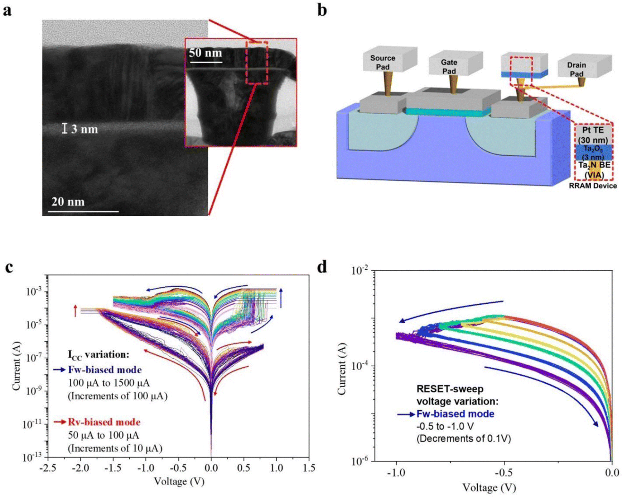 | ||
| Fig. 1 (a) TEM imaging revealed the cross-sectional view of the 1R device, and the (b) schematic of the 1T–1R device (not drawn to scale). The red dotted box shows the zoomed-in cross-sectional view of the 1R scanned by TEM in (a). (c) Multilevel cell obtained by ICC variation in the forward-biased (blue arrows) and reverse-biased (red arrows) mode. (d) Reset-sweep variation was also utilized to obtain a MLC in the forward-biased mode. | ||
Two operating modes are presented in this work, by which the devices were subjected to forward and reverse-biased modes on the same device. In this work, the ground is permanently fixed with respect to the Pt top electrode (TE). As a result, the forward-biased mode requires a positive voltage applied on the bottom electrode (BE) for the set operation and a negative voltage on the BE for the reset operation. Conversely, while in the reverse-biased mode, a negative voltage must be applied on the BE for the set operation; applying a positive voltage on the BE yielded the reset operation. Memristive devices are commonly subjected to an electrical characterization using direct current (DC) I–V double-sweep to elucidate the switching mechanism.21,22 A resultant I–V hysteresis loop is obtained due to the changing current response level caused by the change of potential difference across the devices. Applying the DC I–V double-sweep on the device, a forming voltage is always required to attain the forward-biased mode. The forming process is said to be needed if the current level of the subsequent cycles deviates from the first cycle. In this mode, Fig. 1c reveals the multilevel cell (MLC) switching characteristics of the memristive device. The forward-biased IV curve indicated by the blue arrows shows ten consecutive DC cycles of fifteen sets corresponding to a compliance current (ICC) variation of 0.1 mA to 1.5 mA in increments of 0.1 mA. The set-sweep and reset-sweep voltages were kept constant at 1 V and −1.5 V, respectively. An abrupt jump in the current level was observed in this ICC variation method in the forward-biased mode, in which a larger ICC imposed led to a higher high conductive state (HCS). Imposing an ICC prevents the device from undergoing hard breakdown while halting the movement of conductive ions within the switching layer.5 Additionally, the MLC could also be obtained by varying the reset-sweep voltage. Fig. 1d depicts ten consecutive DC cycles of six sets corresponding to a reset-sweep variation of −0.5 V to −1.0 V. The set-sweep voltage and ICC were kept constant at 1 V and 1 mA, respectively. A gradual decrease in the current level was observed as the absolute value of the reset-sweep voltage increased. There was also no overlap with adjacent states for both the reset-sweep and ICC variation methods in the forward-biased mode. This indicates that the device can store the fifteen and six stable states by leveraging the external ICC and reset-sweep variation, respectively. Fig. 1c also shows that the same device operated in the reverse-biased mode, as indicated by the red arrows. From a pristine state, a negative voltage was applied on the BE to set the device and, conversely, a positive voltage on the BE to reset the device. The devices are observed to not require forming to operate in its reverse-biased mode. Multilevel states were obtained by varying the ICC applied on the device from 50 μA to 100 μA in increments of 10 μA, while the set-sweep and reset-sweep voltages were kept constant at −2.0 V and 0.8 V, respectively. Varying the imposed ICC led to the observation of different conductance states. A higher ICC applied corresponded to a higher current level (conductance levels) during the sweepback in the negative voltage region. A gradual increase in the current level in the HCS was observed as the absolute value of the set-sweep voltage increased before reaching the ICC.
Elucidation of the switching mechanism in both operation modes
As mentioned previously, a forming process is required to operate the device in the forward-biased mode by applying a positive voltage (larger than the set voltage) on the BE. This forming process is also its threshold transition, enabling the device to transition from its reverse-biased mode to its forward-biased mode. This is advantageous practically (i.e., when operating in pulse operation) because the switching voltage in the reverse-biased mode is unlikely to meet the forming voltage threshold during operation. Furthermore, a current range buffer exists between the two switching modes, as shown using the DC-IV curves of the devices, which are below the forward-biased mode and above the reverse-biased mode in Fig. S1b (ESI†). To add clarity to this, Fig. S1c (ESI†) shows the forming voltages of ten different devices featured in this work. Their forming voltages varied from 1.04 V to 1.52 V, with a median value of 1.32 V. The red dotted line depicts the reset voltage in the reverse-biased mode. Since practical applications require demonstration of pulse operation, the marginal difference between the reset voltage in the reverse-biased mode and the forming voltage in the forward-biased mode becomes crucial, as a larger margin prevents unintended transition into the forward-biased mode as long as the reset voltage in the reverse-biased mode does not increase above the forming voltage threshold. This is unlike in most previous studies, in which the memristive hysteresis loop of the gradual switching sits directly above that of the abrupt switching, leading to an absence of the aforementioned current buffer.9,23–28 In other words, in those works, the HCS of the reverse-biased mode is also the low conductive state (LCS) of the forward-biased mode. This would lead to an undesired change in modes during pulse operations, rendering them useless in such applications. Since the devices have distinct differences in current responses, there is a need to understand the physics behind the switching behavior of the different operational modes. An experiment was designed to investigate the influence of the memristive device size in the different modes on the switching current levels.Fig. 2a depicts the HCS and LCS of the devices in the forward-biased mode (blue) and reverse-biased mode (red) in terms of their device size diameter. For the forward-biased mode, the LCS and HCS were obtained with a reading voltage of 0.1 V after a set sweep of 1 V (ICC = 1 mA) and a reset sweep of −1V, respectively. For the reverse-biased mode, the LCS and HCS were acquired by a reading voltage of 0.3 V after a set sweep of −2V (ICC = 100 μA), and the HCS was obtained after a reset sweep of 1V, respectively. The measurement was done over five cycles using five devices each to obtain the mean conductance, and the conductance ranges were then plotted as an interval plot. The results showed that the conductance states in the forward-biased mode are independent of their device sizes. This is shown by the conductance level being relatively constant regardless of the device size. This differs from the reverse-biased mode, whereby the conductance states positively correlate with the size of the devices, i.e., the larger the device area, the higher the conductance states (and also a smaller on–off ratio). Consequently, this suggests that in the forward-biased mode, resistive switching happens locally (due to filament formation). In contrast, in the reverse-biased mode, the device undergoes homogenous switching, which occurs interfacially in the reverse-biased mode. The apparent subsequent step was to identify the location of this interfacial switching through the use of X-ray photoelectron spectroscopy (XPS) depth profile analysis.
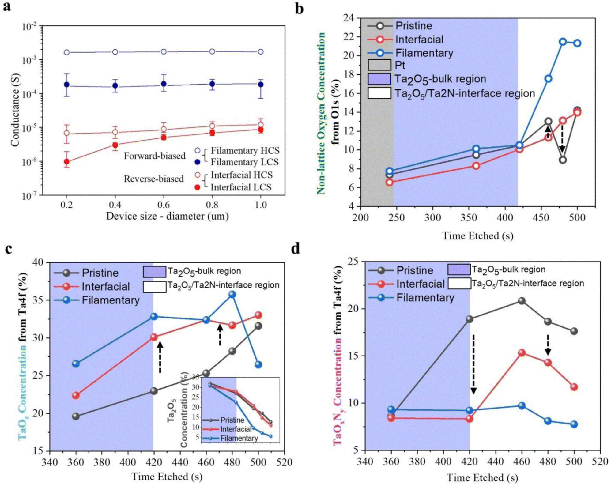 | ||
| Fig. 2 (a) Conductance-size dependence study conducted on the memristive devices shows size independence in the forward-biased (blue) modes and size dependence in the reverse-biased mode. Percentage concentration of (b) non-lattice oxygen from O1s, (c) TaOz from Ta4f, and (d) TaOxNy from Ta4f as obtained by XPS depth profiling (raw data and fittings presented in Fig. S2 and S3, ESI†) | ||
However, due to the scanning limitations of XPS, additional devices fabricated were scaled up in terms of the switching layer thickness (to 35 nm) and device diameter (100 μm). This exact size was chosen because the device switched in the same current range as the original devices in the reverse-biased mode. Three different devices (pristine – sample A [black], interfacial HCS – sample B [red], and filamentary HCS – sample C [blue]) were investigated for their switching mechanism. The fitting of the raw data is presented in Figures S2 and S3 (ESI†) for O1s (528–535 eV) and Ta4f (20–31 eV) peaks, respectively.29–33 The O1s spectra were deconvoluted into two peaks, and Ta4f was deconvoluted into five doublet peaks, respectively.29–33 In terms of the depth profile, there were approximately two regions: <420 s time etched for the Ta2O5 bulk region and the >420 s time etched for the Ta2O5/Ta2N interface region. Fig. 2b shows the concentration percentage of the non-lattice as a percentage of total O1s core level peaks. It could be observed that the level of non-lattice oxygen concentrations increased at relatively the same rates from ∼7% to ∼10% in the bulk region for all three samples. However, this is drastically different in the interface region. Comparing samples A and B, the non-lattice oxygen concentration in sample A dipped to the bulk levels (∼9%) at 480 s etch depth. Conversely, the non-lattice oxygen concentration in sample B continued to increase at the interface until the levels of both samples A and B equalized at 500 s etch depth. This suggests that a depth exists within the interface by which the percentage of lattice oxygen is higher than the depth above and below it. In other words, this is also caused by the redox reaction that happens at the Ta2O5/Ta2N interface. This hypothesis is also further corroborated by TaOz concentration and TaOxNy concentration as a percentage of Ta4f peaks in Fig. 2c and d, respectively. In Fig. 2c, TaOz was detected earlier and had a larger concentration in sample B compared to sample A. Similarly, in Fig. 2d, TaOxNy was detected earlier and had a higher concentration in sample A compared to sample B. Moving on to the analysis of sample C, observations made in Fig. 2b revealed that the non-lattice oxygen concentration percentage in sample C was similar to that of samples A and B in the bulk. However, nearer to the interface, there was a large increase in this non-lattice oxygen concentration percentage. Fig. 2c then shows that sample C contained relatively higher TaOz (Ta suboxide) content percentage-wise compared to samples A and B. This also supported the revelation of the consistently lower Ta2O5 percentage concentration in sample C compared to samples A and B, suggesting a larger amount of oxygen vacancies or defects present throughout the switching layers of the device. Finally, it can also be seen in Fig. 2d that the TaOxNy concentration percentage in sample C remained negligible compared to samples A and B.
In order to further clarify the explanation made from the XPS results in Fig. 2, Fig. 3 was created to depict the proposed switching mechanism of the memristive device in the different modes. Within the literature on the coexistence of filamentary and interfacial switching in memristive devices, the underlying mechanism behind most interfacial switching was proposed to stem from the trapping and de-trapping of charges at the oxide-inert electrode interface, for which the evidence is lacking in some prior works.8,23,24 In this work, we propose that for the Pt/Ta2O5/Ta2N device presented, the interfacial switching happens at the oxide-active electrode interface instead. Fig. 3 illustrates that the interfacial switching of the device in the reverse-biased mode is caused by external electrical stimuli, leading to the thickness modulation of the oxide-active electrode interface. Initially, Ta2N/Ta2O5/Pt layers were deposited. The redox reaction then spontaneously started to proceed at the Ta2O5/Ta2N interface due to the oxygen-gettering tendencies of the tantalum nitride electrode.34,35 The XPS results in Fig. 2 suggest that in the reverse-biased mode, the Ta2O5 layer acts as an oxygen reservoir to enable the redox reaction with the Ta2N layer. The externally applied electric field modulates the TaOxNy and TaOz concentration, sandwiched by the oxidation of the Ta2N layer below and the reduction of the Ta2O5 switching layer. Additionally, the Ta ions from the Ta2N BE are also expected to contribute to the downward growth of the TaOxNy layer due to their upward migration from the Ta2N electrode layer, as shown in a prior study that they are mobile in the Ta2O5 layer and are believed to mediate switching.36 Applying a negative voltage (in the reverse-biased mode) onto the pristine device to set it resulted in the generation of non-lattice oxygen (and, in its place, oxygen vacancies), providing the device with a higher conductance. Conversely, applying a positive voltage brings these oxygen ions back down into the interface, thus increasing the rate of recombination of the oxygen vacancies and thereby reducing the device conductance. This explanation is similar to Baek et al.'s work on the TiN/PCMO/Pt memristor stack, where an in situ TEM was used to prove that the resistive switching was a result of the shrinking and expansion of the TiOxNy interfacial layer.37 For the forward-biased mode, applying a relatively larger positive voltage causes dielectric soft-breakdown. Consequently, it introduces more defects in the form of localized oxygen vacancies throughout the switching layer (also known as the conductive filament). The filamentary switching in the forward-biased mode can be explained by the widely agreed filamentary formation and dissolution model.5,38–40 Previously, in Fig. 1, two typical approaches are implemented to demonstrate the multi-bit capability in the forward-biased mode, i.e., current control during the set operation and voltage control during the reset operation. For the reset operation, as seen in Fig. 3, the entire filament (composed of oxygen vacancies, Vo) disconnected from the TE, resulting in a decreased current level. Subsequently, as the voltage magnitude increased negatively, the filament retracted further from the cathode, causing an additional decrease in the current level. During the set operation, a fine localized filament grows from the BE to TE and gradually expands radially as the current increases. Imposing ICC then allowed for control to obtain multilevel switching, depending on the radial size of the filament, in which larger conductive filament thickness reflects a higher device conductance.
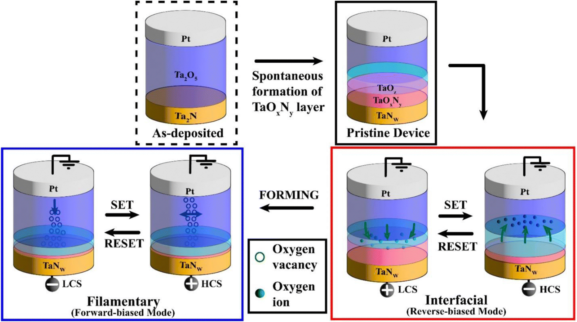 | ||
| Fig. 3 Schematic diagram of the Pt/Ta2O5/Ta2N memristor switching mechanisms in both forward-biased (localized filamentary) and reverse-biased (interfacial) modes. Filamentary switching occurs when the voltage applied across the electrodes controls the migration of oxygen vacancies acting as highly conductive pathways for electrical current flow. The interfacial mode is proposed to happen due to the expansion and contraction of the spontaneously formed TaOxNy dominant layer within the memristive device due to voltage, effectively reducing and increasing device conductance. The transition from interfacial switching to filamentary switching requires a forming process, during which the switching layer undergoes soft-break down and oxygen vacancies are introduced. | ||
Conduction mechanism of the devices in both operation modes
Besides the switching mechanism, it is also crucial to understand the charge transport dynamics within the device during the electrical characterization (i.e., the DC sweep). For example, Ohmic conduction is crucial for executing matrix-vector multiplication by harnessing Kirchhoff's Law, effectively reducing the IR drop in a large array. This effect has also been analogous to the intricacies of the functions of the biological brain.41 Conduction mechanism models reported in the literature are broadly categorized into electrode-limited or bulk-limited.42 The consensus with such analysis is that although there tend to be multiple mechanisms concurrently happening with the device, the fitting to various models only shows the most dominant effect.42 Determining the most dominant mechanism would possibly help develop new applications to exploit the memristor's switching properties during fabrication or tuning. Fig. 4 shows the conduction mechanism of the device, whereby the fitting was done on the device operated in both the forward-biased (Fig. 4a and b) and reverse-biased (Fig. 4c and d) modes. Fig. 4a and b depict the forward-biased IV curves fitted with the Ohmic and Schottky conduction mechanisms, respectively. The insets in these figures show the region/s from which the IV data were collected. Voltage sweeps were applied across the device five times consecutively to ensure that the change in current did not occur due to the change in the conductance state of the device. The gradient and y-axis intercept were then obtained from the average fittings. Generally, the LCS low-field regions showed an ohmic conduction mechanism in both polarities in the range of |0 to 0.2 V|. This was revealed through a double arithmetic fitting with an average gradient of 1.05 and 1.07 for positive and negative polarities, respectively. Under a low field, only a small number of carriers are generated through thermal excitation. The data points in the LCS high-field region deviated from the fittings; hence, other conduction mechanism models were fitted instead. The Schottky model (shown in eqn (1)) was the best fit through a ln I against V1/2 fitting for the data points in that region. When the device is subjected to a relatively higher electric field, an increase in thermal energy further excites the electrons, allowing them to overcome the Schottky energy barrier at the interfaces to enter the dielectric layer. This happens until a point where the set voltage is reached, and the device undergoes an abrupt resistive state switch into the HCS. Experimental dielectric constant values of 37.2 and 47.7 were obtained for the positive and negative sweeps, respectively, and the Schottky barrier height was 2.09 eV for both the Ta2N/TaOxNy and Ta2O5/Pt interfaces. For both positive and negative polarities in the HCS region, the double logarithmic fitting was again the best fit, with an average gradient of 1.05 in both regions. This low field coincides with the read voltage, which is beneficial when the devices are in an array-level in-memory computing implementation, and that is to avoid non-idealities like the sneak path or leakage current when dealing with positively non-linear loads (where the current through the device increases more than being proportionate with an increase in voltage).43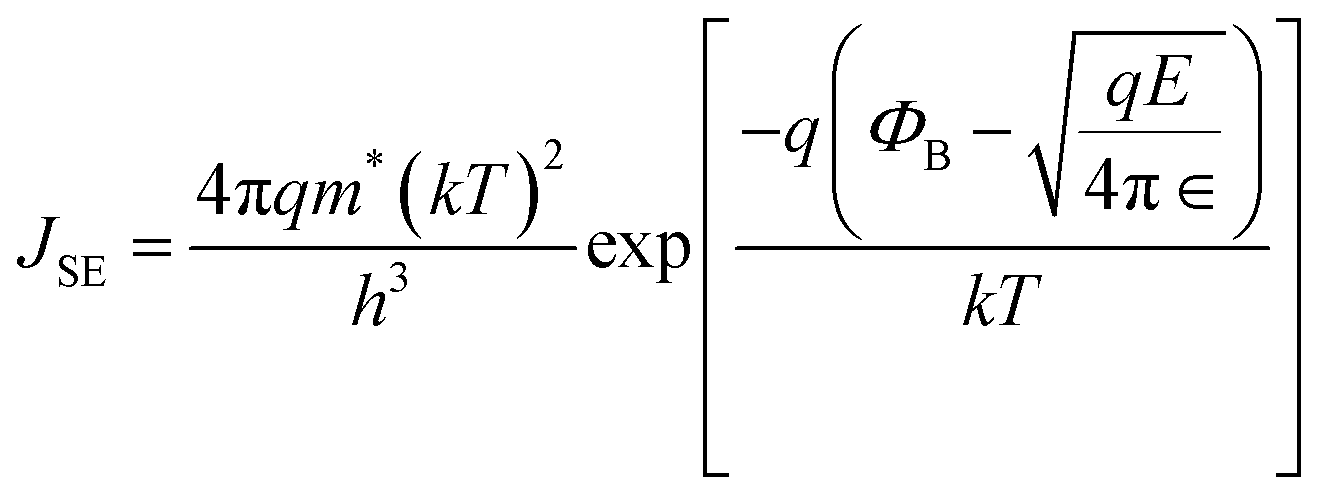 | (1) |
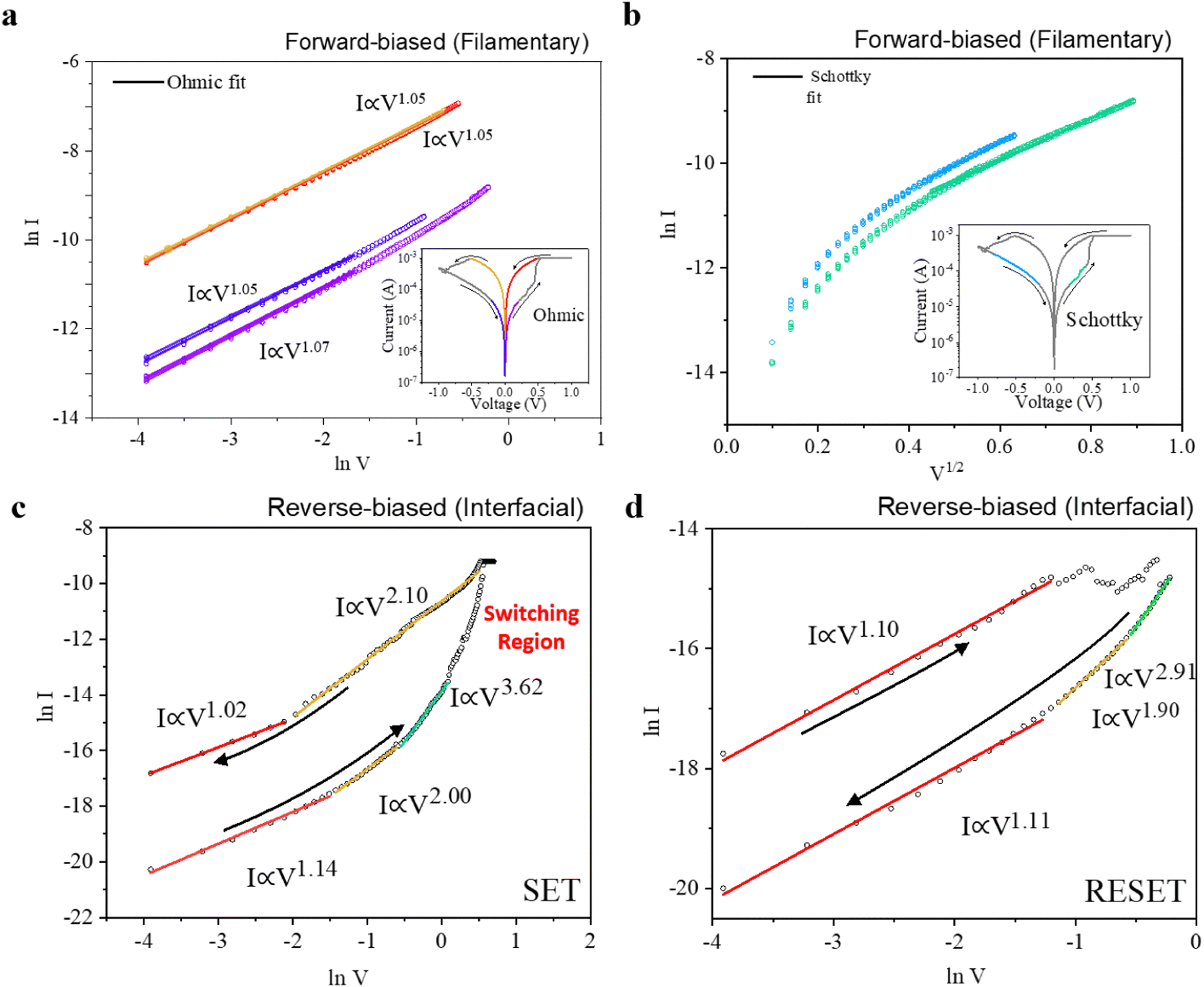 | ||
| Fig. 4 Fitting and analysis of the DC I–V curve using a double logarithmic plot forward-biased mode indicated that it is dominated by (a) Ohmic mechanism in the low-field LCS and HCS, and (b) Schottky mechanism in the high-field LCS. The I–V characteristic device in its reverse-biased mode indicates an SCLC conduction mechanism for the (c) set process and the (d) reset process, in which all of the fitting ones were with adjusted R2 values of more than 0.99. | ||
Fig. 4c and d then depict the set and reset IV curves in the reverse-biased mode, respectively. In Fig. 4c, increasing the voltage in the reverse-biased LCS region, the slope of the ln-ln curve evolved from a gradient of 1.14 in the low-field region (0 to −0.22 V, red) to a gradient of 2.00 (−0.22 V to −0.54 V, orange), and then finally to a gradient of 3.62 in the high-field region (> −0.54 V). When the voltage was swept back, the current response initially gave a gradient of 2.10 and subsequently back to 1.02 in the low field. The fitting in Fig. 4d then showed a similar trend in the reset operation, in which, from its LCS, the curve gradient started from 1.10, and then a decrease in current was eventually observed at −0.28 V. The sweep back at a higher field of > −0.56 in the LCS led to the gradient undergoing a transition from 2.91 from a high-field region to a gradient of 1.90 (−0.28 V to −0.56 V), then finally to a gradient of 1.11 in the low field region (0 to −0.28 V). The discussed results suggest that the space-charge limited conduction (SCLC) mechanism was the dominant conduction mechanism when operated in the reverse-biased mode, in which the slopes of the graph at different regions correspond to the Ohmic law (∼I ∝ V) at low field, a transition to the Mott–Gurney law (∼I ∝ V2), and finally a steep increase in current injection at higher fields (∼I ∝ V>2).42 To explain from the LCS, when the device was subjected to a low field in its LCS, it was in the ohmic state. In this range, the density of the thermally generated free carriers within the switching layer was larger than that of the injected carriers. As the voltage was then increased, the traps within the switching layer started to fill up, and the slope of the curve was interpreted to follow the Mott–Gurney law. These traps were fully filled as the device was swept with a high field. This correlated with an accelerated increase of the current level whereby further injected carriers were freely moving within the layer.44 For all the best-fit lines done in this work, adjusted R2 values were always more than 0.99.
From fitting the Schottky emission model in eqn (1) to Fig. 4b, the gradient and y-axis intercept were extracted to be ∼4.47 and ∼−12.3 for the positive region, and ∼3.95 and ∼−12.3 for the negative region. The dielectric constants and Schottky barrier heights were derived from those values. Depending on the deposition methods and parameters, Ta2O5 thin films generally have a dielectric constant around the range of 25; however, they can go upwards to 110, as reported by Lin et al.45,46 On the other hand, TaOz has a dielectric constant that is generally lower than Ta2O5. In this work, we obtained an experimental value of ∼37.2 and ∼47.7 for the positive and negative sweeps, respectively. This suggests that the effective dielectric constant of the dielectric layer, which was sandwiched by the electrodes, decreased during the set operation and increased during the reset operation. Referring back to the filamentary switching mechanism schematic in Fig. 3, the percentage of TaOz is increased due to the generation of non-lattice oxygen during the set process and decreased due to the recombination of these non-lattice oxygen species. This would lead to a drop and increase in the effective dielectric constant, respectively, consistent with TaOz having a lower dielectric constant than the more stoichiometric Ta2O5, as mentioned previously. Fig. 5a summarises the findings using an energy band diagram, in which the values in red were calculated based on this experiment, and those in brackets were both polarities, which were calculated to be 2.09 eV. Using these values, the electron affinity of the TaOz/TaOxNy and Ta2O5 layers was determined to be 2.11 eV and 3.55 eV, respectively. Therefore, the evidence suggests the existence of Schottky barriers at both interfaces as obtained from the literature.47,48 As mentioned previously, eqn (1) was utilized to obtain the Schottky barrier height of the devices in both polarities, which was calculated to be 2.09 eV. Using these values, the electron affinity of the TaOz/TaOxNy and Ta2O5 layers was determined to be 2.11 eV and 3.55 eV, respectively. Therefore, the evidence suggests the existence of Schottky barriers at both interfaces.
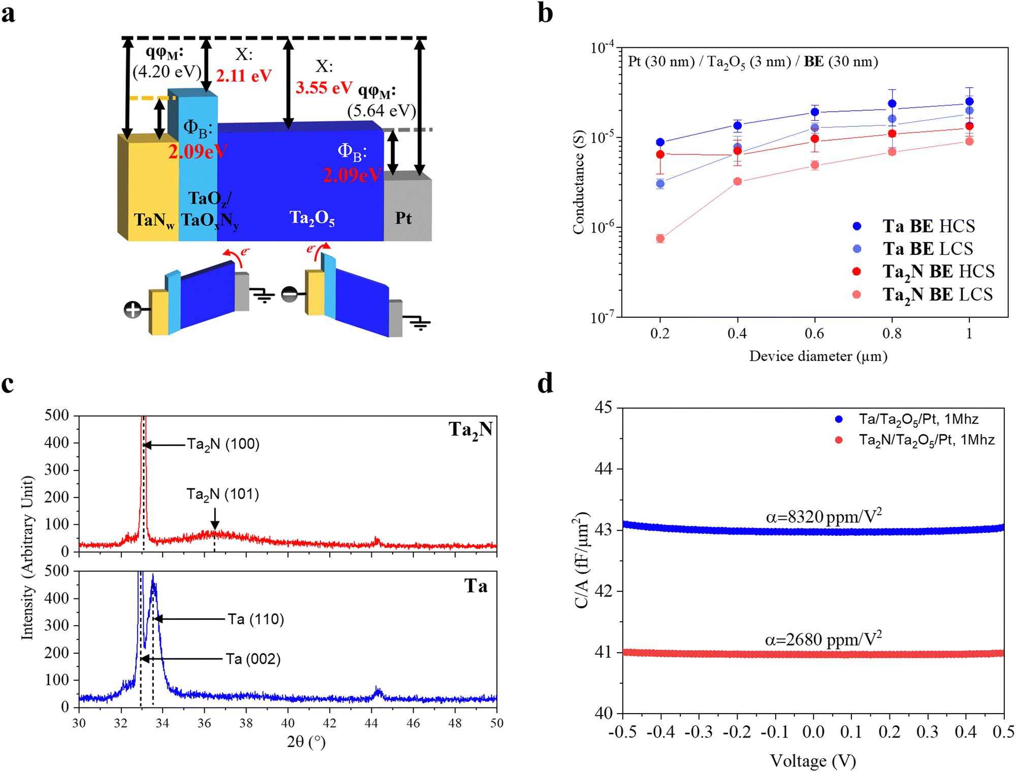 | ||
| Fig. 5 (a) Schematic band diagram of the deposited Pt/Ta2O5/Ta2N memristor. (b) Comparison of the effects of changing the BE from Ta2N (red) to Ta (blue). Investigation of the LCS and HCS of 5 devices for each device diameter. Ta BE devices constantly had a device conductance lower than that of those with the Ta2N active BE. (c) XRD pattern of Ta2N and Ta deposited on a SiO2 substrate, showing that the Ta deposited was one of a beta phase, with a dominant (002) peak and a relatively weaker peak at (110). Reactive sputtering with nitrogen yielded a strong Ta2N peak at (100) and a weak peak at (101). (d) C–V characteristics of Pt/Ta2O5/Ta2N and Pt/Ta2O5/Ta. | ||
To provide further elucidation on the conduction and switching mechanisms mentioned above, it is necessary to begin from the pristine device shown in Fig. 3. When a negative biased (reverse-biased mode, Fig. 4c) is applied to the device, it undergoes SCLC, a bulk-limited conduction mechanism, due to which as the applied voltage across the device is increased negatively, the rate of increase of current also increases. This results in a decrease of resistance across the Ta2O5 bulk, with the majority of the voltage being shifted to the TaOxNy/TaOz interface, where switching is proposed to commence. This effect is shown in Fig. S4 (ESI†), where the I–V curve starts to exhibit a hysteresis above > ∼1.0 V (as shown in Fig. S4, ESI†). This hysteresis gets larger as we continue to increase the said voltage. Subsequently, during the forming process to transition the device to the filamentary forward-biased mode, the oxygen vacancies form a low-resistance filament in the Ta2O5 bulk, connecting the two electrodes. This is where the device conduction starts to be governed by the Schottky mechanism, an electrode/interface-limited conduction mechanism.
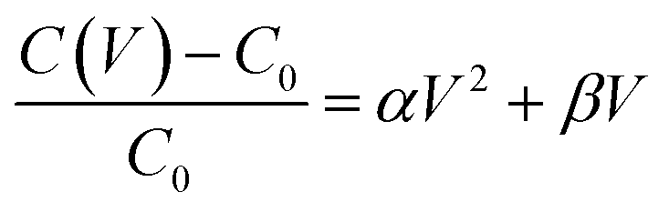
Besides the switching layers having a direct impact on the switching characteristics, there is also much evidence of the electrode engineering affecting the device switching characteristics.49–53 Hence, it was also important to delve into how the nitrogen content in the BE helps with the switching characteristics of the proposed Pt/Ta2O5/Ta2N devices. Fig. 5b shows a conductance plot for the memristive devices with Ta2N (red) and Ta (blue) as the BE, operated in the DC reverse-biased mode. Five devices were measured for each device size, and the conductance variations were accounted for as error bars within each data point. The devices were switched with a set and reset voltage of −2 V and 1 V, respectively, and an ICC of 100 μA was imposed during the set operation. The devices' states were read with a reference voltage of 0.1 V. It was then observed that the respective HCS and LCS are consistently higher for the Ta BE devices than for the Ta2N BE. This could be attributed to either the nitrogen content in the BE contributing to the series resistance of the memristive device, or the difference in oxygen affinities of the different BE layers altering the oxygen content of the Ta2O5 switching layer directly above, or both. X-ray diffraction (XRD) was subsequently performed on 30 nm of both Ta and Ta2N, and its results are depicted in Fig. 5c. The BE materials were deposited via sputtering onto SiO2 substrates to confirm the BE material as claimed. It was then observed in the resultant XRD patterns that the Ta that was deposited by sputtering had a strong β-Ta 002 peak at around 32.9° and a relatively weaker α-Ta 110 peak at around 33.5°.54 Comparatively, the sputter-deposited Ta2N had a strong hex-Ta2N 100 peak at 33.0° and another relatively weak hex-Ta2N 101 peak at 36.8°.55 After observing that the film deposited by reactive sputtering was that of a hex-Ta2N, capacitance–voltage (C–V) measurement was conducted on the Pt/Ta2O5/Ta and Pt/Ta2O5/Ta2N memristive devices, for which the results are presented in Fig. 5d. The C–V analysis was conducted by fitting the second-order polynomial C–V equation to obtain the voltage coefficient of capacitance (VCC) shown in eqn (2):56–58
 | (2) |
1T–1R integration of the Ta2O5-based memristor and performance
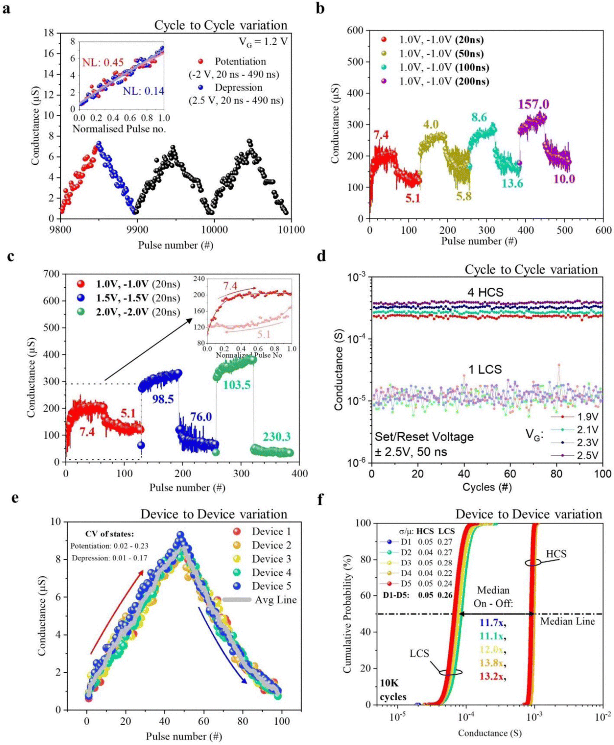
The Ta2O5 memristive device in this work was then integrated into the N-channel metal–oxide semiconductor field effect transistor (NMOS) transistor at its drain. Integrating the 1T–1R cell structure allows data to be stored using the memristor element while simultaneously using the NMOS transistor to control the current across the memristive device, thus reducing the sneak current when presented in an array. In this work, the NMOS transistor is also exploited to demonstrate the control of the multilevel cell properties of the memristive devices during practical (pulse) operations. Referring back to the 1T–1R schematic in Fig. 1b, in the forward-biased mode of the 1T–1R cell, the set process was conducted by applying a positive voltage on the source pad, and the reset operation was conducted by applying a positive voltage on the TE pad. Conversely, the reverse-biased mode required a positive voltage on the TE pad for the set operation and a positive voltage on the source pad for the reset operation. Consequently, the reference voltage and current will be with respect to the source of the transistor for the presentation of this work below (and TE considered grounded). Positive voltage was also applied on the gate pad to turn on the transistor. The multilevel switching characteristics of the 1T–1R integrated device were also demonstrated under the DC scheme with the variation of the VG and VS, as shown in Fig. S4 (ESI†).Fig. 6a depicts the potential of the reverse-biased mode for synaptic weight tuning (e.g., neuromorphic computing) applications. The best demonstration of this application came from applying a series of 96 pulses on the 1T–1R integrated device. These pulses simulate the increasing (48 pulses) and decreasing (48 pulses) weights within an artificial neural network (ANN). In particular, a gradual increase in pulse width was applied for both potentiation and depression (20 ns to 490 ns) while keeping the pulse amplitude equal throughout (−2 V and 2.5 V for potentiation and depression, respectively). In total, >106 increasing and decreasing pulses were conducted on the device in this described method, and this is depicted in Fig. S5a (ESI†) and will be further discussed in the reliability section below. A series of 96 pulses was subjected to the nonlinearity (NL) analysis to investigate the application further quantitatively, in which the data fitted to the following equations:48
| GLTP = Gmin + B(1 − e−AP) | (3) |
| GLTD = Gmax + B(1 − eA(P−1)) | (4) |
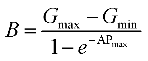 | (5) |
 | ||
| Fig. 6 1T–1R operation of the Pt/Ta2O5/Ta2N device in the reverse-biased mode, and synaptic weight characteristics when applying increasing pulse width from 20 ns to 490 ns. This was compared to operating in the forward-biased mode, where the pulse widths and amplitudes were varied and shown in (b) and (c), respectively. The device was also investigated for its memory applications by operating in the forward-biased mode for binary switching shown in (d), and five states were obtained when varying the VG from 1.9 V to 2.5 V and switching parameters of 2.5 V for 50 ns. Device to device variation of (e) potentiation and depression in the reverse-biased mode, and (f) binary switching in the forward-biased mode showing low variation between five devices. | ||
Additionally, Fig. 6e and f depict the device-to-device variation in both reverse and forward-biased modes using five devices each. In Fig. 6e, the potentiation and depression curves of five devices were overlapped while operated in the reverse-biased mode, and the coefficient of variability (CV, or σ/μ) was calculated for each of the 98 states. The CV of the potentiation pulses ranged from 0.02 to 0.23, while the depression pulses ranged from 0.01 to 0.17, showing low deviation of data in each state. The devices were then formed and operated in their forward-biased modes, and all were used to run 10 K cycles each. Fig. 6f shows these 10 K cycles in the form of a cumulative probability plot. Both the LCS and HCS showed low CV, and when comparing inter-device and intra-devices, the CV showed negligible differences. The on–off ratio between the LCS and HCS is also about ∼12.5 times, meaning that it was still easy to differentiate between the on and off states in the forward-biased mode.
Device reliability
Retention and endurance measurements were conducted to investigate the reliability of the devices discussed in this work. Fig. 7a depicts the retention reliability of the Pt/Ta2O5/Ta2N memristive device structures. The conductance states of a single device were switched (via DC measurements, parameters shown in Fig. 7a) at room temperature while being subjected to temperature stress at 85 °C for 104 s for each state. The memristive device was subjected to temperature stress from a pristine condition. It was observed that the conductance state of this pristine device dropped to sub-μS during this stage. Subsequently, during the reading of the reverse-biased LCS, the device's conductance rose from about 50 s; nevertheless, it reached a stable state above the pristine stressed conductance. Hence, the device was seen to have good retention, and its conductance states remained stable with minimum fluctuations when subjected to temperature stress. The device was also characterized for its endurance, as shown in Fig. 7b, by operating identically to Fig. 6d, whereby 2.5 V and −2.5 V pulses were applied for 50 ns for set and reset operations (and VG = 2.0 V) in the forward-biased mode. Resultant states were read at 0.1 V for 100 μs for every cycle. The device was observed to be able to switch for >106 cycles with stable HCS. However, the LCS tended to fluctuate around 10−4 to 10−5 S. The endurance in the reverse-biased mode is also shown in Fig. S5a (ESI†), by which operating identically to the method to obtain results shown in Fig. 6a, the device continued to work even after >106 pulses (>10![[thin space (1/6-em)]](https://www.rsc.org/images/entities/char_2009.gif) 204 potentiation and depression complete cycles). Figures S5b to S5f (ESI†) show the evolution of the PD cycles over the 106 pulses, three sets for every order of PD cycles. The NL factor was utilized to quantify the degradation of the device, shown by the fitting in the inset in the aforementioned figures. It was also shown that there were some ∼1000 pulses that should be run before the device would settle in the optimum state in this application, exhibiting an NL factor of <2, and after ten cycles, this improved to a value of <1. Further PD cycles displayed an even more significantly improved NL factor of <0.5 before showing some decline in the potentiation NL factor to >2 after 103 PD cycles. Nevertheless, its depression NL factor remained at an excellent level of <0.5. At 104 PD cycles, an overall reduction of the total conductance range caused a more significant degradation in the NL factor of <3. Additionally, the devices were also shown to have a possibility of reversibility, and the method to achieve this is shown in Fig. S7 (ESI†).
204 potentiation and depression complete cycles). Figures S5b to S5f (ESI†) show the evolution of the PD cycles over the 106 pulses, three sets for every order of PD cycles. The NL factor was utilized to quantify the degradation of the device, shown by the fitting in the inset in the aforementioned figures. It was also shown that there were some ∼1000 pulses that should be run before the device would settle in the optimum state in this application, exhibiting an NL factor of <2, and after ten cycles, this improved to a value of <1. Further PD cycles displayed an even more significantly improved NL factor of <0.5 before showing some decline in the potentiation NL factor to >2 after 103 PD cycles. Nevertheless, its depression NL factor remained at an excellent level of <0.5. At 104 PD cycles, an overall reduction of the total conductance range caused a more significant degradation in the NL factor of <3. Additionally, the devices were also shown to have a possibility of reversibility, and the method to achieve this is shown in Fig. S7 (ESI†).
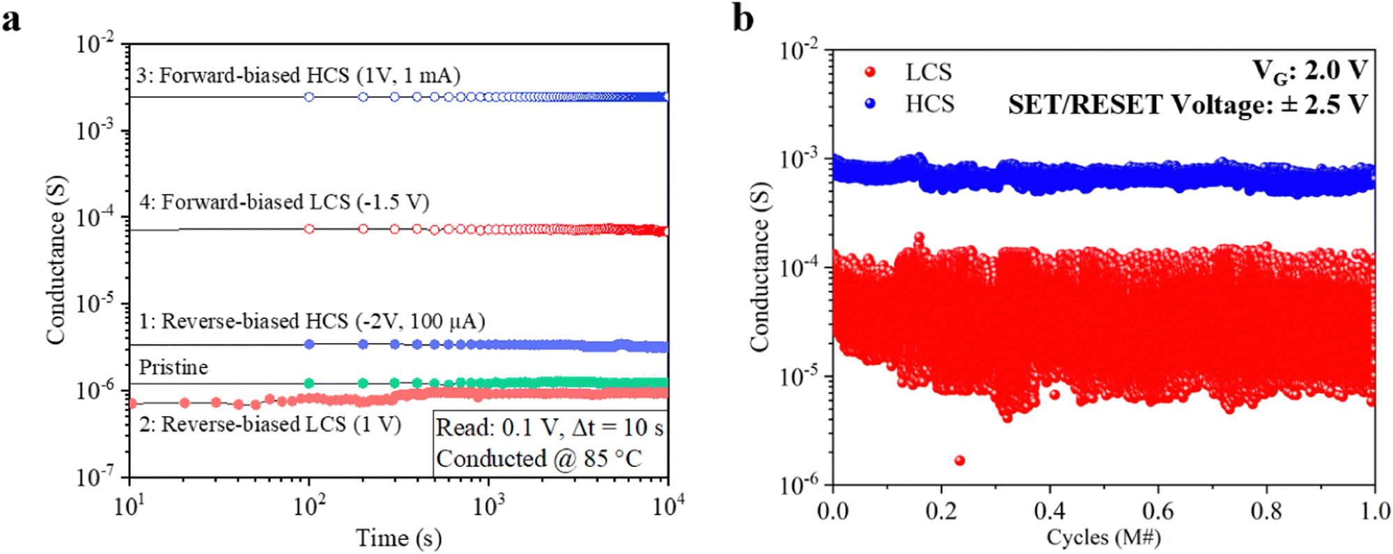 | ||
| Fig. 7 (a) Retention characteristics of the memristive device show good retention under temperature stress at 85 °C for 104 s. (b) Endurance characterization of switching under 2.5 V and −2.5 V pulses applied for 50 ns for set and reset operations (and VG = 2.0 V) in the forward-biased mode. Resultant states were read at 0.1 V for 100 μs for every cycle. The device was observed to be able to switch for >106 cycles with stable LCS and HCS. | ||
Comparison with past works
Table 1 summarizes the comparative analysis of the performance and reliability of devices that exhibit the coexistence of abrupt and gradual switching characteristics presented in this work and those investigated by similar studies in the existing literature. Unlike this work, devices with such duality of modes are not typically explored for practical applications due to the challenges associated with the unintended switching between modes. Nevertheless, our proposed memristive device boasts a lower forming voltage (1.32 V) and lower switching voltage (±2.5 V) relative to the faster switching speed (50 ns). Our device size is also comparably one of the smallest and operates in a lower current range, affirming its potential for further scalability within array integration. Additionally, our devices demonstrate reliability, adhering to industry standards, with stable retention adhering to standards of 104 s at 85 °C. They also exhibit excellent endurance of > 106 set and reset cycles, which was tested with endurance characterization methods recommended by Lanza et al.61 In essence, compared to past studies, this work showcases the robustness of our devices, offering a combination of performance, reliability, and scalability when operated in both forward and reverse-biased modes.| Memristor structure (thickness [nm]) | Device size | Switching performance | Reliability | Ref. | |||
|---|---|---|---|---|---|---|---|
| V Forming (V) | V Set (V)/VReset (V)/(Switching speed [if avail]) c | I CC (mA) | Endurance (cycles) | Retention | |||
| a The exact forming voltage was not mentioned. b Initially conductive. c Values reported under DC characterization if not explicitly mentioned. d I CC imposed with the use of the NMOS transistor. e LRS drift under the gradual switching scheme; other states remain stable. | |||||||
| Au/Sr2TiO4(10)/Nb:SrTiO3 | 100–400 μm | 2–3 | −4 V/4 V (gradual) | 10 | NA. | NA. | 26 |
| 4 V/−10 V (gradual) | |||||||
| Pt(100)/Fe:SrTiO3(500)/Nb:SrTiO3(substrate) | 10 μm | 12 | −2.2 V/2.8 V (gradual) | 2 | NA. | NA. | 62 |
| 2.8 V/−3.5 V (abrupt) | |||||||
| W/graded Wox(15–160)/Pt(70) | 190–250 nm | −2.2 | Pulsed: 1.2 V/−1.6 V (1 μs) (abrupt) | 10 | 2000 | 104 s @ 85 °C e | 6,24 |
| −1 V/1.25 V (1 ms) (gradual) | |||||||
| TiN/DyMn2O5(10)/Pt | N.A. | Yes a | 1 V/−1.8 V (abrupt) | 10 | 100 | 104 s @ 85 °C | 63 |
| −1.8 V/0.6 V (gradual) | |||||||
| Pt(100)/ZnO(100)/Pt(100) | 50–200 μm | 2.8 | −2 V/2 V (gradual, bipolar) | 10 | 100 | 104 s @ 85 °C e | 64 |
| 1.5 V/0.7 V (abrupt, unipolar) | 100 | ||||||
| Pt (20)/Ti(10)/TiO2(3–6)/Pt | 60–100 nm | No b | −3.5 V/1.7 V (abrupt) | 0.1 | NA. | 1.26 × 10⁴ s @ 85 °C | 28 |
| 1.7 V/−3.5 V (gradual) | |||||||
| Pulsed: −2.1 V (100 ns) (abrupt) | |||||||
| 2.2 V (100 μs) (gradual) | |||||||
| Pt(30)/Ta2O5(3)/Ta2N | 100 nm | 1.32 | 0.7 V/−1 V (abrupt) | 1 | 106 | 104 s @ 85 °C | This work |
| −2 V/0.8 V (gradual) | 0.1 | ||||||
| Pulsed: 2.5 V/−2.5 V (abrupt) | <0.1 d | ||||||
| −2 V/0.8 V (gradual) | |||||||
Conclusions
In summary, a Ta2O5-based memristive device has been proposed and demonstrated for the coexistence of localized and interfacial switching characteristics within a single device, operated in its forward or reverse-biased mode, respectively. A conductance size-dependence study then revealed the size-independent characteristics of the localized (filamentary) switching states, while interfacial switching states exhibited a size-dependent behavior. Additionally, we proposed and proved that the interfacial switching behavior happened due to the modulation of the oxygen-deficient interfacial layers sandwiched between the active Ta2N electrode and the Ta2O5 oxide layers. Furthermore, the active electrode (Ta2N) was chosen due to the reduced oxygen affinity compared to Ta, enabling the filamentary switching within the memristive device. The integration of the 1T–1R device demonstrated its capability as a non-volatile memory element in the forward-biased filamentary mode and a synaptic weight-tuning unit in the reverse-biased non-filamentary mode. The devices showed great endurance of >106 cycles and pulses in both forward and reverse-biased modes, respectively. The conductance states of the device also exhibited stable states with minimal fluctuations under temperature stress at 85 °C for 104 s. Overall, achieving dual modes within the same device presented in this work unveils the suitability of the device as a unified memory solution.Methodology
Device fabrication
For the 1T1R integration, a foundry-obtained chip containing NMOS transistor was patterned with electron-beam lithography (EBL) and etched with reactive ion etching (RIE) to access the Ta2N via. A 3 nm-ultrathin Ta2O5 switching layer was then deposited by 50 W RF magnetron sputtering at 2 mTorr pressure with 20 sccm Ar gas flow, followed by deposition of a 15 nm Pt top electrode by 50 W DC magnetron sputtering at the same pressure and gas flow.For the 1R device size variation experiments (Fig. 2a and 5b), a 30 nm Ta2N was first blanket-deposited on a SiO2 wafer as a common layer with reactive radio frequency (RF) magnetron sputtering at 4 mTorr pressure with 26 sccm of Ar and 4 sccm of N2 gas, resulting in Ta2N with a sheet resistivity of 270 μΩ-cm (measured with a four-point technique).65 The resultant layer was identical to the Ta2N from the via in the 1T1R chip. Following this, a 30 nm Si3N4 passivation layer was deposited using plasma-enhanced chemical vapor deposition (PE-CVD). An EBL step was subsequently done to pattern circular holes that varied from 200 nm to 1 μm. RIE was then used to etch the patterned hole of Si3N4 at a rate of 1 nm s−1. The e-beam resist was removed, and another lithography step was done to pattern the top electrode. The 3 nm Ta2O5 switching layer and 30 nm Pt TE were then deposited with steps identical to the 1T1R process to fill in the hole which is connected to the Pt.
Materials and device characterisation
For bulk characterization, XPS was conducted by utilizing the Kratos Analytical Axis Supra Plus XPS system.For surface and topology characterization studies, the non-contact mode of the Park Systems NX1 AFM was utilized to scan the electrode surfaces, and the XRR and XRD measurements were performed using the Rigaku SmartLab with the Cu Kα radiation.
The electrical I–V and C–V characterization studies of the devices were conducted using the Keithley 4200A-SCS semiconductor parameter analyzer.
Author contributions
E. K. K. and P. A. D. conceptualized this work. E. K. K. contributed to most of the work, including research methodology, data curation, formal investigation, and data visualization. H. Y. P. assisted in performing XRD and XRR measurements. P. A. D., H. Y. P., L.L., C. X. X. L., and J. R. T. contributed to the formal analysis of the results. Y. S. Y. and W. S. L. supervised the research. W. S. L. acquired the funds for this research work. E. K. K. drafted the manuscript. All authors reviewed and revised the manuscript.Conflicts of interest
There are no conflicts to declare.Acknowledgements
This work was supported by a RIE2020 ASTAR AME IAF-ICP Grant (No. I1801E0030). We would also like to acknowledge Dr Teddy Salim from the Facility for Analysis, Characterisation, Testing and Simulation, Nanyang Technological University, Singapore, for the assistance in ultilizing the X-ray facilities.References
- D. Ielmini and H. S. P. Wong, Nat. Electron., 2018, 1, 333–343 CrossRef.
- W. Zhang, B. Gao, J. Tang, X. Li, W. Wu, H. Qian and H. Wu, Phys. Status Solidi RRL, 2019, 13, 1–13 Search PubMed.
- S. C. W. Chow, P. A. Dananjaya, J. M. Ang, D. J. J. Loy, J. R. Thong, S. W. Hoo, E. H. Toh and W. S. Lew, Appl. Surf. Sci., 2023, 608, 155233 CrossRef CAS.
- P. A. Dananjaya, D. J. J. Loy, S. C. W. Chow and W. S. Lew, ACS Appl. Electron. Mater., 2019, 1, 2076–2085 CrossRef CAS.
- T. S. Lee, N. J. Lee, H. Abbas, H. H. Lee, T.-S. Yoon and C. J. Kang, ACS Appl. Electron. Mater., 2020, 2, 1154–1161 CrossRef CAS.
- K. P. Biju, X. Liu, M. Siddik, S. Kim, J. Shin, I. Kim, A. Ignatiev and H. Hwang, J. Appl. Phys., 2011, 110, 064505 CrossRef.
- M. Kim, M. A. Rehman, D. Lee, Y. Wang, D.-H. Lim, M. F. Khan, H. Choi, Q. Y. Shao, J. Suh, H.-S. Lee and H.-H. Park, ACS Appl. Mater. Interfaces, 2022, 14, 44561–44571 CrossRef CAS PubMed.
- H. Ryu and S. Kim, Nanomaterials, 2020, 10, 2055 CrossRef CAS PubMed.
- A. Schönhals, C. M. M. Rosário, S. Hoffmann-Eifert, R. Waser, S. Menzel and D. J. Wouters, Adv. Electron. Mater., 2018, 4, 1700243 CrossRef.
- C. La Torre, A. Kindsmüller, D. J. Wouters, C. E. Graves, G. A. Gibson, J. P. Strachan, R. S. Williams, R. Waser and S. Menzel, Nanoscale, 2017, 9, 14414–14422 RSC.
- A. Sebastian, M. Le Gallo, R. Khaddam-Aljameh and E. Eleftheriou, Nat. Nanotechnol., 2020, 15, 529–544 CrossRef CAS PubMed.
- S. Yu, W. Shim, X. Peng and Y. Luo, IEEE Trans. Circuits Syst. Regul. Pap., 2021, 68, 2753–2765 Search PubMed.
- S. Cho, J. Jung, S. Kim and J. J. Pak, Semicond. Sci. Technol., 2020, 35, 085006 CrossRef CAS.
- L. Liu, P. A. Dananjaya, C. C. I. Ang, E. K. Koh, G. J. Lim, H. Y. Poh, M. Y. Chee, C. X. X. Lee and W. S. Lew, Nanoscale, 2023, 15, 17076–17084 RSC.
- L. Liu, P. A. Dananjaya, M. Y. Chee, G. J. Lim, C. X. X. Lee and W. S. Lew, ACS Appl. Mater. Interfaces, 2023, 15, 29287–29296 CrossRef CAS PubMed.
- M. Prezioso, F. Merrikh-Bayat, B. D. Hoskins, G. C. Adam, K. K. Likharev and D. B. Strukov, Nature, 2015, 521, 61–64 CrossRef CAS PubMed.
- C. Li, D. Belkin, Y. Li, P. Yan, M. Hu, N. Ge, H. Jiang, E. Montgomery, P. Lin, Z. Wang, W. Song, J. P. Strachan, M. Barnell, Q. Wu, R. S. Williams, J. J. Yang and Q. Xia, Nat. Commun., 2018, 9, 2385 CrossRef PubMed.
- M. Zhao, B. Gao, J. Tang, H. Qian and H. Wu, Appl. Phys. Rev., 2020, 7, 011301 CAS.
- W. Wan, R. Kubendran, C. Schaefer, S. B. Eryilmaz, W. Zhang, D. Wu, S. Deiss, P. Raina, H. Qian, B. Gao, S. Joshi, H. Wu, H.-S. P. Wong and G. Cauwenberghs, Nature, 2022, 608, 504–512 CrossRef CAS PubMed.
- W.-H. Chen, C. Dou, K.-X. Li, W.-Y. Lin, P.-Y. Li, J.-H. Huang, J.-H. Wang, W.-C. Wei, C.-X. Xue, Y.-C. Chiu, Y.-C. King, C.-J. Lin, R.-S. Liu, C.-C. Hsieh, K.-T. Tang, J. J. Yang, M.-S. Ho and M.-F. Chang, Nat. Electron., 2019, 2, 420–428 CrossRef CAS.
- B. Tang, H. Veluri, Y. Li, Z. G. Yu, M. Waqar, J. F. Leong, M. Sivan, E. Zamburg, Y.-W. Zhang, J. Wang and A. V. Y. Thean, Nat. Commun., 2022, 13, 3037 CrossRef CAS PubMed.
- J. Jian, P. Dong, Z. Jian, T. Zhao, C. Miao, H. Chang, J. Chen, Y.-F. Chen, Y.-B. Chen, H. Feng and B. Sorli, ACS Nano, 2022, 16, 20445–20456 CrossRef CAS PubMed.
- R. Muenstermann, T. Menke, R. Dittmann and R. Waser, Adv. Mater., 2010, 22, 4819–4822 CrossRef CAS PubMed.
- K. P. Biju, X. Liu, S. Kim, S. Jung, J. Park and H. Hwang, Phys. Status Solidi RRL, 2011, 5, 89–91 CrossRef CAS.
- S. Yun, J. Park, M. Kang and S. Kim, Results Phys., 2022, 34, 105307 CrossRef.
- K. Shibuya, R. Dittmann, S. Mi and R. Waser, Adv. Mater., 2010, 22, 411–414 CrossRef CAS PubMed.
- F. Miao, J. Joshua Yang, J. Borghetti, G. Medeiros-Ribeiro and R. Stanley Williams, Nanotechnology, 2011, 22, 254007 CrossRef PubMed.
- H. Zhang, S. Yoo, S. Menzel, C. Funck, F. Cüppers, D. J. Wouters, C. S. Hwang, R. Waser and S. Hoffmann-Eifert, ACS Appl. Mater. Interfaces, 2018, 10, 29766–29778 CrossRef CAS PubMed.
- M. Ismail, H. Abbas, A. Sokolov, C. Mahata, C. Choi and S. Kim, Ceram. Int., 2021, 47, 30764–30776 CrossRef CAS.
- K. X. Shi, H. Y. Xu, Z. Q. Wang, X. N. Zhao, W. Z. Liu, J. G. Ma and Y. C. Liu, Appl. Phys. Lett., 2017, 111, 223505 CrossRef.
- R. Simpson, R. G. White, J. F. Watts and M. A. Baker, Appl. Surf. Sci., 2017, 405, 79–87 CrossRef CAS.
- S. Khan, M. J. M. Zapata, M. B. Pereira, R. V. Gonçalves, L. Strizik, J. Dupont, M. J. L. Santos and S. R. Teixeira, Phys. Chem. Chem. Phys., 2015, 17, 23952–23962 RSC.
- D. Cristea, L. Cunha, C. Gabor, I. Ghiuta, C. Croitoru, A. Marin, L. Velicu, A. Besleaga and B. Vasile, Nanomaterials, 2019, 9, 476 CrossRef CAS PubMed.
- Q. Zhou and J. Zhai, Phys. Status Solidi A, 2014, 211, 173–179 CrossRef CAS.
- M. Ismail, E. Ahmed, A. M. Rana, I. Talib, T. Khan, K. Iqbal and M. Y. Nadeem, Thin Solid Films, 2015, 583, 95–101 CrossRef CAS.
- A. Wedig, M. Luebben, D.-Y. Cho, M. Moors, K. Skaja, V. Rana, T. Hasegawa, K. K. Adepalli, B. Yildiz, R. Waser and I. Valov, Nat. Nanotechnol., 2016, 11, 67–74 CrossRef CAS PubMed.
- K. Baek, S. Park, J. Park, Y.-M. Kim, H. Hwang and S. H. Oh, Nanoscale, 2017, 9, 582–593 RSC.
- P. Huang, X. Y. Liu, W. H. Li, Y. X. Deng, B. Chen, Y. Lu, B. Gao, L. Zeng, K. L. Wei, G. Du, X. Zhang and J. F. Kang, Int. Electron Devices Meet., 2012, 26.6.1–26.6.4 Search PubMed.
- Y. D. Zhao, P. Huang, Z. Chen, C. Liu, H. T. Li, B. Chen, W. J. Ma, F. F. Zhang, B. Gao, X. Y. Liu and J. F. Kang, in 2015 International Symposium on VLSI Technology, Systems and Applications, 2015, 1–2.
- C. Cai, S. Wei, Z. Yin, J. Bai, W. Xie, Y. Li, F. Qin, Y. Su and D. Wang, Appl. Surf. Sci., 2021, 560, 149960 CrossRef CAS.
- B. Widrow, Y. Kim, D. Park and J. K. Perin, Artificial Intelligence in the Age of Neural Networks and Brain Computing, ed. R. Kozma, C. Alippi, Y. Choe and F. C. Morabito, Academic Press, 2019, pp. 1–30 Search PubMed.
- F.-C. Chiu, Adv. Mater. Sci. Eng., 2014, 2014, 578168 Search PubMed.
- W. Banerjee, Electronics, 2020, 9, 1029, DOI:10.3390/electronics9061029.
- A. Lekshmi Jagath, C. Hock Leong, T. N. Kumar and H. F. Almurib, J. Eng., 2019, 2019, 4644–4652 CrossRef.
- J. Lin, N. Masaaki, A. Tsukune and M. Yamada, Appl. Phys. Lett., 1999, 74, 2370–2372 CrossRef CAS.
- D. Cristea, A. Crisan, N. Cretu, J. Borges, C. Lopes, L. Cunha, V. Ion, M. Dinescu, N. P. Barradas, E. Alves, M. Apreutesei and D. Munteanu, Appl. Surf. Sci., 2015, 354, 298–305 CrossRef CAS.
- C. S. Kang, H.-J. Cho, Y. H. Kim, R. Choi, K. Onishi, A. Shahriar and J. C. Lee, J. Vac. Sci. Technol., B: Microelectron. Nanometer Struct.--Process., Meas., Phenom., 2003, 21, 2026–2028 CrossRef CAS.
- CRC handbook of chemistry and physics, CRC Press, 103th edn, Rumble, J. R., Ed.; CRC Press, 2022 Search PubMed.
- X. Li, H. Wu, B. Gao, W. Wu, D. Wu, N. Deng, J. Cai and H. Qian, Nanotechnology, 2016, 27, 305201 CrossRef PubMed.
- L. Goux, A. Fantini, Y. Y. Chen, A. Redolfi, R. Degraeve and M. Jurczak, ECS Solid State Lett., 2014, 3, Q79 CrossRef CAS.
- V. Y.-Q. Zhuo, Y. Jiang, M. H. Li, E. K. Chua, Z. Zhang, J. S. Pan, R. Zhao, L. P. Shi, T. C. Chong and J. Robertson, Appl. Phys. Lett., 2013, 102, 062106 CrossRef.
- L. Goux, A. Fantini, A. Redolfi, C. Y. Chen, F. F. Shi, R. Degraeve, Y. Y. Chen, T. Witters, G. Groeseneken and M. Jurczak, in 2014 Symposium on VLSI Technology (VLSI-Technology): Digest of Technical Papers, 2014, pp. 1–2.
- C. Sun, S. M. Lu, F. Jin, W. Q. Mo, J. L. Song and K. F. Dong, J. Alloys Compd., 2018, 749, 481–486 CrossRef CAS.
- A. Jiang, T. A. Tyson, L. Axe, L. Gładczuk, M. Sosnowski and P. Cote, Thin Solid Films, 2004, 479, 166–173 CrossRef.
- A. Zaman and E. I. Meletis, Coatings, 2017, 7, 209 CrossRef.
- K. C. Chiang, C. H. Cheng, H. C. Pan, C. N. Hsiao, C. P. Chou, A. Chin and H. L. Hwang, IEEE Electron Device Lett., 2007, 28, 235–237 CAS.
- C. Wenger, M. Lukosius, H.-J. Müssig, G. Ruhl, S. Pasko and C. Lohe, J. Vac. Sci. Technol., B: Microelectron. Nanometer Struct.--Process., Meas., Phenom., 2009, 27, 286–289 CrossRef CAS.
- C. H. Cheng, H. H. Hsu, W. B. Chen, A. Chin and F. S. Yeh, Electrochem. Solid-State Lett., 2009, 13, H16 CrossRef.
- T. Kim, H. Son, I. Kim, J. Kim, S. Lee, J. K. Park, J. Y. Kwak, J. Park and Y. Jeong, Sci. Rep., 2020, 10, 11247 CrossRef CAS PubMed.
- A. Schonhals, A. Kindsmuller, C. L. Torre, H. Zhang, S. Hoffmann-Eifert, S. Menzel, R. Waser and D. J. Wouters, IEEE International Memory Workshop, 2017, 1–4 Search PubMed.
- M. Lanza, R. Waser, D. Ielmini, J. J. Yang, L. Goux, J. Suñe, A. J. Kenyon, A. Mehonic, S. Spiga, V. Rana, S. Wiefels, S. Menzel, I. Valov, M. A. Villena, E. Miranda, X. Jing, F. Campabadal, M. B. Gonzalez, F. Aguirre, F. Palumbo, K. Zhu, J. B. Roldan, F. M. Puglisi, L. Larcher, T.-H. Hou, T. Prodromakis, Y. Yang, P. Huang, T. Wan, Y. Chai, K. L. Pey, N. Raghavan, S. Dueñas, T. Wang, Q. Xia and S. Pazos, ACS Nano, 2021, 15, 17214–17231 CrossRef CAS PubMed.
- D. Cooper, C. Baeumer, N. Bernier, A. Marchewka, C. La Torre, R. E. Dunin-Borkowski, S. Menzel, R. Waser and R. Dittmann, Adv. Mater., 2017, 29, 1700212 CrossRef PubMed.
- Y.-T. Tsai, T.-C. Chang, W.-L. Huang, C.-W. Huang, Y.-E. Syu, S.-C. Chen, S. M. Sze, M.-J. Tsai and T.-Y. Tseng, Appl. Phys. Lett., 2011, 99, 092106 CrossRef.
- C.-H. Huang, J.-S. Huang, C.-C. Lai, H.-W. Huang, S.-J. Lin and Y.-L. Chueh, ACS Appl. Mater. Interfaces, 2013, 5, 6017–6023 CrossRef CAS PubMed.
- H. Y. Poh, C. C. I. Ang, T. L. Jin, F. N. Tan, G. J. Lim, S. Wu, F. Poh and W. S. Lew, Appl. Phys. Lett., 2022, 121, 012405 CrossRef CAS.
Footnote |
| † Electronic supplementary information (ESI) available. See DOI: https://doi.org/10.1039/d3nh00554b |
| This journal is © The Royal Society of Chemistry 2024 |