
Sublimation-based wafer-scale monolayer WS2 formation via self-limited thinning of few-layer WS2†
Mingxi
Chen
 a,
Jianwei
Chai
a,
Jing
Wu
a,
Haofei
Zheng
ab,
Wen-Ya
Wu
a,
James
Lourembam
a,
Ming
Lin
a,
Jun-Young
Kim
a,
Jaewon
Kim
a,
Kah-Wee
Ang
ab,
Man-Fai
Ng
c,
Henry
Medina
*a,
Shi Wun
Tong
*a and
Dongzhi
Chi
*a
a,
Jianwei
Chai
a,
Jing
Wu
a,
Haofei
Zheng
ab,
Wen-Ya
Wu
a,
James
Lourembam
a,
Ming
Lin
a,
Jun-Young
Kim
a,
Jaewon
Kim
a,
Kah-Wee
Ang
ab,
Man-Fai
Ng
c,
Henry
Medina
*a,
Shi Wun
Tong
*a and
Dongzhi
Chi
*a
aInstitute of Materials Research and Engineering (IMRE), Agency for Science, Technology and Research (A*STAR), 2 Fusionopolis Way, Innovis #08-03, Singapore 138634, Republic of Singapore. E-mail: henry.medinasilva@imec.be; tongsw@imre.a-star.edu.sg; dz-chi@imre.a-star.edu.sg
bDepartment of Electrical and Computer Engineering, National University of Singapore, 4 Engineering Drive 3, Singapore 117583, Republic of Singapore
cInstitute of High Performance Computing (IHPC), Agency for Science, Technology and Research (A*STAR), 1 Fusionopolis Way, #16-16 Connexis, Singapore 138632, Republic of Singapore
First published on 5th October 2023
Abstract
Atomically-thin monolayer WS2 is a promising channel material for next-generation Moore's nanoelectronics owing to its high theoretical room temperature electron mobility and immunity to short channel effect. The high photoluminescence (PL) quantum yield of the monolayer WS2 also makes it highly promising for future high-performance optoelectronics. However, the difficulty in strictly growing monolayer WS2, due to its non-self-limiting growth mechanism, may hinder its industrial development because of the uncontrollable growth kinetics in attaining the high uniformity in thickness and property on the wafer-scale. In this study, we report a scalable process to achieve a 4 inch wafer-scale fully-covered strictly monolayer WS2 by applying the in situ self-limited thinning of multilayer WS2 formed by sulfurization of WOx films. Through a pulsed supply of sulfur precursor vapor under a continuous H2 flow, the self-limited thinning process can effectively trim down the overgrown multilayer WS2 to the monolayer limit without damaging the remaining bottom WS2 monolayer. Density functional theory (DFT) calculations reveal that the self-limited thinning arises from the thermodynamic instability of the WS2 top layers as opposed to a stable bottom monolayer WS2 on sapphire above a vacuum sublimation temperature of WS2. The self-limited thinning approach overcomes the intrinsic limitation of conventional vapor-based growth methods in preventing the 2nd layer WS2 domain nucleation/growth. It also offers additional advantages, such as scalability, simplicity, and possibility for batch processing, thus opening up a new avenue to develop a manufacturing-viable growth technology for the preparation of a strictly-monolayer WS2 on the wafer-scale.
New conceptsIn this manuscript, a sublimation-assisted and self-limited thinning approach for wafer-scale transition metal dichalcogenides (TMDCs) is demonstrated for the first time. Tungsten dichalcogenide (WS2) – a promising TMDC-based channel material for next-generation Moore's nanoelectronics is selected as a typical example. Based on sulfurization with pulsed sulfur gas supply and constant H2/Ar gas flow, the thinning effect coming from the volatile reduced WS2−x phase by H2 under a temperature substantially above the sublimation temperature of WS2 can become self-limited. Importantly, the self-limited nature of the thinning process enables the damage-free and strictly monolayer TMDCs formation. This new thinning process simplifies the current challenges in preparing the high-quality monolayer TMDCs, where an inevitable partial oxidation and physical damages associated from conventional etching processes severely degrade the film stoichiometry and uniformity. Notably, the universality of the self-limited thinning effect is also manifested on a broader number of different TMDCs (e.g. MoS2) and TMDCs prepared under various growth approaches (e.g. PVD sputtered WS2 and MoS2) and doped TMDCs system (e.g. Co-doped WS2 prepared by sulfurization). The findings indicate that this thinning method is broadly applicable to pure and doped TMDCs systems, which will accelerate the research of TMDCs with high PL quantum yield and adjustable band gap for large-area optoelectronics and spin-electronics. |
Introduction
As the feature size of silicon-based transistors is approaching their physical limit, there have been intensive efforts in searching for alternative channel materials for future ultra-scaled electronic devices.1,2 The unique thickness-dependent properties of semiconducting 2D layered transition metal dichalcogenides (TMDCs), including WS2, MoS2, WSe2, and MoSe2, make them very attractive for applications in future electronics, optoelectronics, and smart sensors.3–5 The lower effective mass of WS2 among other TMDC semiconductors provides it with the highest theoretical room temperature electron mobility.6–8 In addition, its immunity to the short channel effect, transferability for vertical stacking, and high PL quantum yield make the monolayer WS2 as a promising channel material for sub-3 nm ultra-scaled field effect transistors (FETs) and for high-performance optoelectronics.9,10Over the last 5 and more years, there has been significant progress in the effort for growing large-area atomically thin 2D TMDCs, including WS2. Among the various growth methods developed, including chemical vapor deposition (CVD), metal organic chemical vapor deposition (MOCVD), physical vapor deposition (PVD), and molecular beam epitaxy (MBE),11–13 CVD and MOCVD are considered as the two most promising front-runners in terms of the quality of the grown TMDCs layer and the wafer-size for uniform growth. Both are able to grow monolayer TMDCs on the wafer-scale (up to 4 inch wafer for CVD and up to 8 inch wafer for MOCVD).14,15 However, both CVD and MOCVD also have their own shortcomings for adoption in scalable mass-production. For CVD, where metal oxide (e.g., WO3, MoO3etc.) powders are typically used as metal precursors, it is difficult to further scale up the wafer-size due to its so-called distance-dependent growth mechanism.16,17 In comparison, MOCVD offers a good control over the area uniformity, and therefore greatly improved scalability.18 However, an un-acceptably long growth time (more than 26 h) is required to achieve monolayer growth.19
Other than those limits associated with the individual growth methods, a more general issue with almost all TMDCs growth arises from the difficulty in controlling the layer number. Unlike graphene growth, which is governed by a catalytically driven self-limiting growth mechanism, the CVD/MOCVD/PVD/MBE growth of TMDCs is non-self-limiting growth.20,21 The 2nd layer nucleation/growth occurs after substantial growth of the 1st layer domains, typically at the centers of domains, due to competition between lateral vs. vertical growth, or at their grain boundaries after their coalescence.22–24 This poses a serious challenge for their consistent and robust usage in nanoelectronics since the presence of 2nd layer domains change the electronic structure in TMDCs (since the electronic structure of the bilayer TMCDs is significantly different from monolayer TMDCs), consequently resulting in variation of the device parameters and affecting circuit yields.25–27
Alternative approaches based on the post-growth treatments (e.g., low-power oxygen plasma,28,29 laser thinning method,30 XeF2 gas etching,31etc.) were also used to achieve monolayer TMDCs. Promising thinning effects had been demonstrated by trimming down the few-layer TMDCs designated areas to atomically-thick layers. However, there are also several limitations in these approaches. First, partial oxidation happens on the post-treated TMDCs due to the thinning process being performed under ambient conditions. Such ambient air oxidation would induce uncontrollable doping in TMDCs with O2, H2O or N2, and it is necessary to perform extra sulfurization on post-treated TMDCs to restore their stoichiometry. Second, the etching results are highly sensitive to the exposure time and power of the oxygen plasma, laser beam, and XeF2 etchant gas. More importantly, these post-etching methods are not self-limiting, and it is thus very challenging to avoid the occurrence of physical damages and complete etching on the thinnest TMDCs areas.26,31
Here, we present the use of an in situ self-limited thinning of few-layer WS2 formed by the sulfurization of WOx (W) for the growth of a wafer-scale fully-covered strictly-monolayer WS2. This approach plays with the thermodynamic instability of the WS2 top layers as opposed to the stable bottom monolayer WS2 on suitable substrates (with strong interface coupling), especially in its reduced state, i.e., WS2−x, above the vacuum sublimation temperature of WS2 as revealed in Density functional theory (DFT) simulations. However, we also found that the alternating switching between thinning and non-thinning via a pulsed supply of sulfur precursor vapor in a constant flow of H2 and Ar gas is essential for process robustness and reliability. Strictly-monolayer high quality WS2 films have been prepared successfully on 4 inch substrates using this method with excellent uniformity. The grown monolayer WS2 was further examined by optical microscopy, Raman microscopy, photoluminescence (PL), X-ray photoelectron spectroscopy (XPS) and transmission electron microscopy (TEM) to reveal its high quality. A number of FETs were fabricated on the synthesized monolayer WS2 to demonstrate its potential application in electronics and optoelectronics. Other than overcoming the major intrinsic limitation of conventional vapor-based growth methods in preventing the 2nd layer WS2 domain nucleation and growth, additional potential advantages of the self-limited thinning approach could also include: (1) scalability (growth area is determined by the original sputter-deposited WOx (or W) film coverage); (2) simplicity in process methodologies (the use of industry-standard sputter-deposition and conventional sulfurization); and (3) possibility for batch processing (several WOx(W)-deposited wafers can be processed simultaneously in a large growth reactor).
Results and discussion
In our sulfurization and subsequent self-limited thinning for the formation of monolayer WS2, a pre-deposited WO3 (thickness of 1–3 nm) film on sapphire is placed in the downstream heating zone of a furnace with an appropriate temperature (e.g., 1000 °C) and pressure (e.g., ∼10 Torr). Diethyl sulfide (DES, (C2H5)2S) (as liquid sulfur precursor) is diluted by carrier gas Ar with a precise control of the concentration through regulating the bubbler and mass flow controller, while a constant flow of Ar + H2 mixed etching gas is also fed into the reaction chamber, as illustrated in Fig. 1a (see the Method section for the detailed growth conditions). Different from the growth of WS2via conventional sulfurization of a pre-deposited WO3 film with a constant sulfur source (CSS) supply, a typical self-limited thinning process for the WS2 monolayer formation features a pulsed sulfur supply (PSS) under a constant Ar + H2 mixed gas flow. Fig. 1b details the DES supply and process temperature temporal profiles in a typical PSS WS2 monolayer formation process cycle, where the DES supply is switched ON and OFF 3 times under 2 stages of high temperature processing (the 1st stage involves a linear temperature ramp-up period (20 min) from 600 °C to 1000 °C and the 2nd stage involves the annealing at 1000 °C for another 30 min). Fig. 1c shows the optical image of a fully-covered WS2 film grown on a 4 inch (0001)-Al2O3 sapphire wafer by the PSS method. Micro-Raman and PL measurements were performed on different regions of the WS2 film to assess the thickness (i.e., layer number) and PL property on the corresponding positions and analyze their area uniformity across the 4 inch wafer (Fig. 1d and e). Fig. 1d compares the Raman spectra obtained on different regions on the wafer. No noticeable variations in peak positions and intensities are observed for the two signature Raman peaks, i.e., E2g (in-plane mode) and A1g (out-of-plane mode). It is known that both the intensity ratio of A1g/E2g and the frequency difference (Δω) between the E2g and A1g peaks increase with the increasing number of layers in WS2 films.19 Thus, the observation of essentially identical values of the A1g/E2g intensity ratio and Δω from the Raman spectra obtained on the different positions clearly indicates excellent thickness uniformity in the grown WS2 film over the entire 4 inch wafer. The values of the A1g/E2g intensity ratio and Δω are ∼0.7 and ∼61.5 cm−1, respectively, and are in good agreement with that reported for the monolayer WS2,32 as well as that measured on the monolayer WS2 single crystal (Fig. S1a and b, ESI†),11 suggesting that the grown WS2 is mostly or even completely covered by a monolayer WS2 area. The formation of the monolayer WS2 is further evidenced by the observation of a strong PL peak at ∼1.98 eV with the peak intensity as high as that from the single crystal monolayer WS2 (Fig. S1c, ESI†). It should be noted that, in WS2, only the direct bandgap monolayer WS2 exhibits a strong PL emission (at ∼1.98 eV), as opposed to weak PL emissions from the indirect bandgap bilayer and multilayer WS2.33,34 Furthermore, the emission intensity of the PL peak essentially remains the same for the different positions on the wafer, again indicating excellent uniformity of the WS2 film formed across the wafer.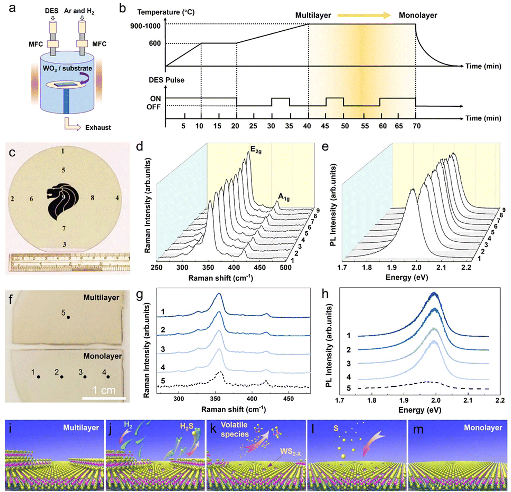 | ||
| Fig. 1 Sublimation-based wafer-scale monolayer WS2 formation via self-limited thinning of few-layer WS2. (a) A schematic configuration showing the position of the WO3-coated substrate, gas flow of DES, Ar and H2 carrier gas inside the vertical furnace tube. (b) Illustrations of the temporal profiles of the process temperature and DES supply for a typical PSS process growth cycle consisting of three DES turn-on pulse cycles. (c) Photograph of the as-grown PSS-WS2 film on the 4-inch sapphire wafer. (d) Raman and (e) PL spectra collected on 9 different positions of the as-grown PSS-WS2 film on the 4-inch sapphire wafer. (f) Photographs of the WS2 sample grown in the midway (top) and completion (bottom) of the PSS process growth cycle. (g) Raman and (h) PL spectra collected on different positions of the WS2 films, as shown in (f). Schematic drawings showing the growth mechanism of the PSS-WS2: (i) multi-layer WS2 growth in the early low-temperature stage, (j) reduction of the top few-layer WS2, (k) sublimation into the volatile WS2−x species (thinning effect), (l) sulfur diffusion to restore WS2−x back to stable WS2 on sapphire and (m) strictly monolayer WS2 formation. | ||
As mentioned earlier, the demonstration of the wafer-scale monolayer WS2 formation shown in Fig. 1c is based on the sublimation-assisted and self-limited thinning process of few-layer WS2. Indeed, an apparent color difference can be seen from the photographs of WS2 films grown in the midway (top) and completion (bottom) of the PSS process growth cycle (Fig. 1f) due to the variation of the bandgap in WS2 of different thicknesses. The large value of Δω (∼64 cm−1) and small PL emission suggested that the WS2 grown in the midway of the PSS growth cycle (the state after ramping up from 600 °C to 1000 °C in PSS process) was few-layer thick (measured on spot 5 in Fig. 1g and h). Comparatively, a monolayer WS2 would be formed if its growth cycle went through the entire PSS process, as evidenced by the value of Δω ∼ 61.5 cm−1 (spots 1–4 in Fig. 1g) and strong PL emission at 1.98 eV (spots 1–4 in Fig. 1h). In short, the self-limited thinning PSS process consisted of 5 steps: (1) multi-layer WS2 growth in the early low-temperature stage, (2) reduction of the top few-layer WS2, (3) sublimation into the volatile WS2−x species (thinning process), (4) sulfur diffusion to restore WS2−x back to stable WS2 on sapphire, and (5) a formation of stable and strictly monolayer WS2 (Fig. 1i–m). The detailed growth mechanism will be discussed with XPS, TEM and DFT results in the later sessions. Notably, the self-limited thinning PSS process can also be manifested on PVD-sputtered WS2 (Fig. S2, ESI†) and MoS2 (Fig. S3, ESI†), in which the few-layer regions are trimmed down into strictly-monolayer with full surface coverage. In addition, this PSS monolayer WS2 method can be extended to the large area uniform formation of doped W1−x(Mx)S2 monolayer, as revealed by our preliminary work with Co doping (Fig. S4, ESI†). These findings are an embodiment of the universality of the self-limited thinning effect in the PSS process.
The as-grown PSS-WS2 films were transferred onto a SiO2/Si substrate for further examination through a conventional van der Waals 2D layer transfer method.35Fig. 2a indicates the optical microscope image of a transferred monolayer WS2 film on the substrate of SiO2/Si, while Fig. 2b shows the mapping image of the PL peak intensity over the red dashed box region in Fig. 2a. The homogeneous color contrast shown from the mapping image suggests that the transferred WS2 film maintains a high degree of integrity with minimum defects. This is further confirmed by AFM measurement (Fig. 2c), where a surface roughness (Rq) as low as 0.212 nm is obtained without revealing any evidence of the presence of bilayer domains. The height profile along the blue-dotted line indicates that the thickness of WS2 is about 0.65 nm, agreeing well with the reported value (∼0.67 nm) for monolayer WS213 and thus unambiguously confirming that a strictly monolayer WS2 is indeed prepared by the PSS sulfurization and subsequent self-limited thinning process. TEM characterization was carried out to reveal the crystalline structure of the transferred monolayer WS2 (Fig. 2d and e). Excellent uniformity of the monolayer WS2 is evident from the TEM image (over 60 nm × 60 nm), where neither bilayer regions nor grain boundaries are present. A well-defined atomic arrangement is observable in the High-Resolution TEM image, indicating a high crystallinity of WS2. The measured d-spacing of the (1010) planes are about 0.27 nm, which coincides well with the reported value for 2H-WS2.36 To assess its single crystallinity, selected-area electron diffraction (SAED) was performed on four different locations (over μm-scale area) of the monolayer WS2 (Fig. 2f). As shown in Fig. 2f, each pattern shows one set of six hexagonal dots, indicating high crystal crystallinity, while all of the patterns present an almost identical lattice orientation, suggesting the presence of large grains in μm scale.
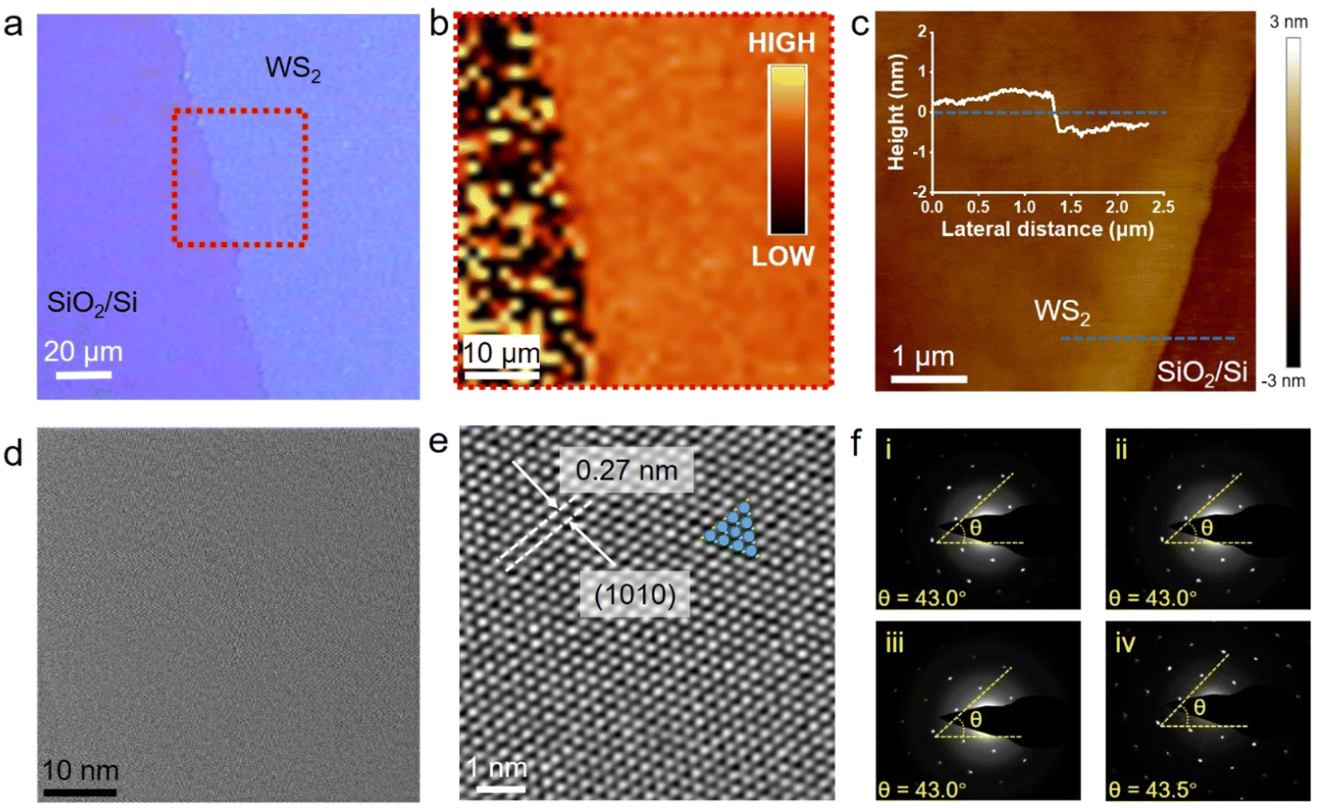 | ||
| Fig. 2 Characterizations of the transferred PSS-WS2 on the substrates of SiO2/Si and TEM grid. (a) Optical microscope image, (b) mapping image based on the PL intensity of PSS-WS2 (enclosed by the red dotted-line in (a)) and (c) plane-view AFM image. The inset in (c) shows the thickness of PSS-WS2 along the dashed line in the AFM image. TEM images acquired under (d) low-resolution and (e) high-resolution of the monolayer PSS-WS2. (f) Representative SAED patterns collected from four typical locations of the continuous monolayer WS2 revealing nearly the same lattice orientation; the yellow dashed line guides the orientation between the six hexagonal dots and horizontal direction. | ||
With the formation of monolayer WS2 by the self-limited PSS process being confirmed by the experimental results presented above, X-ray photoelectron spectroscopy (XPS) was carried out to analyze the phase evolution in the original WOx film during/after the CSS and PSS process to gain insight of the monolayer formation mechanism (Fig. 3a). It was found that the sulfurization of the WOx film at 600 °C during the initial stage of the CSS and PSS process (for 10 min, see Fig. 1b) resulted in a substantial, but incomplete conversion of WOx to WS2. This is evident from the observation of three W 4f core-level peaks (i.e., two dominant W 4f7/2 (∼32.8 eV) and W 4f5/2 (∼35 eV)) and a faint W 5p3/2 (∼37.9 eV) (peaks) corresponding to WS2, together with two weak W 4f peaks (W 4f7/2 (∼36.1 eV) and W 4f5/2 (∼38.2 eV)) from WO3. Cross-section TEM of the 600 °C-sulfurized film indeed confirms the partial formation of few-layer WS2 (2–4 layers) on top, while a substantial amount of residual WOx remains beneath the WS2 formed (Fig. 3c–e). It is seen that the WOx phase remains even after further sulfurization at a much higher temperature of 1000 °C under a constant DES supply, i.e., CSS process (Fig. 3a), presumably due to the effective inhibition of S penetration by the top WS2 multilayer.
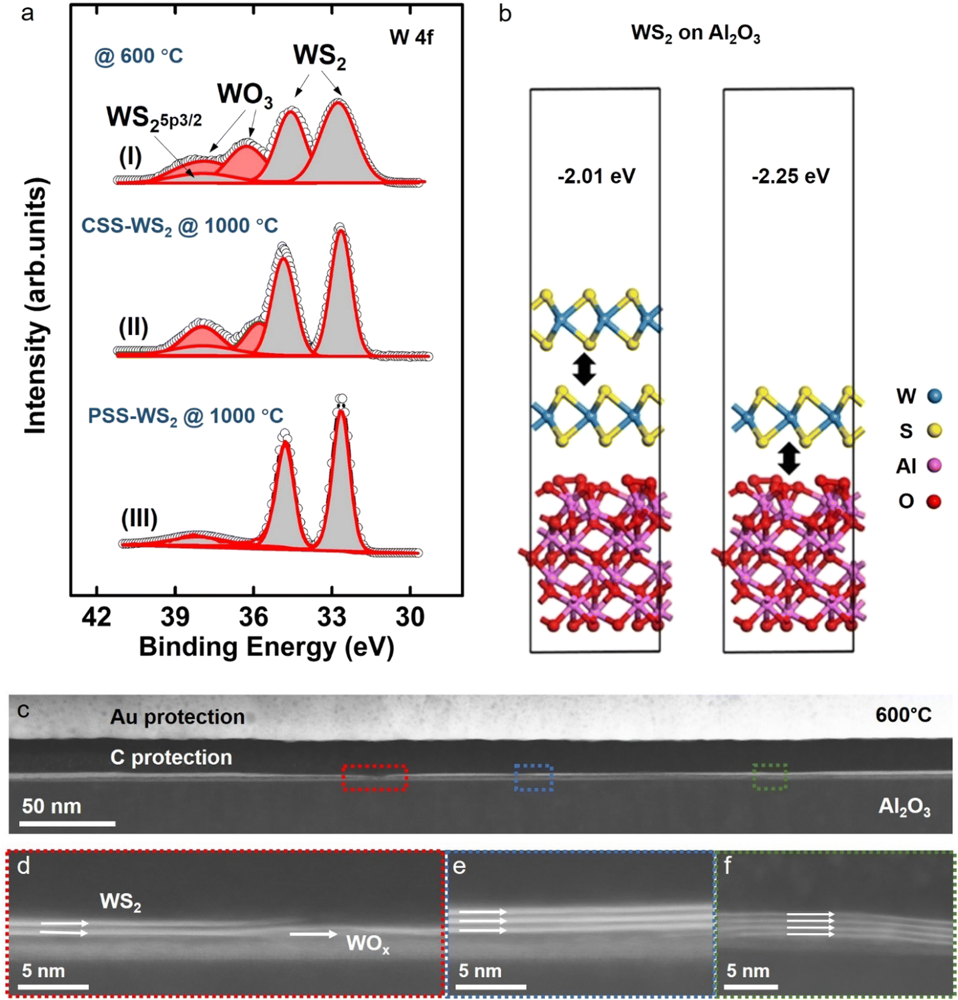 | ||
| Fig. 3 Self-limiting thinning mechanism of monolayer WS2 on the sapphire. (a) W 4f peaks of XPS spectra of WS2 growth under different conditions: (I) sulfur supply at 600 °C, (II) constant sulfur supply at 1000 °C, (III) pulsed sulfur supply at 1000 °C, (b) Slab structures of monolayer (right) and bilayer (left) WS2 on Al2O3. (c) Cross-sectional STEM image acquired at low magnification at the interface of WS2/sapphire prepared under sulfur supply at 600 °C. (d)–(f) The corresponding zoomed-in images were captured over three different areas enclosed by the dotted rectangles. | ||
The multilayer nature of CSS-WS2 is revealed by its much larger A1g/E2g ratio of ∼0.6, which agrees with reported results,37 and significantly weaker PL intensity as compared to PSS-WS2 (Fig. 4a and b), which may also lead to a higher roughness of the CSS-WS2 surface (Fig. S5, ESI†). An apparent discrepancy in film color can also be observed from the photographs of the CSS-WS2 and PSS-WS2 films (Fig. 4c and d) due to the variation of the bandgap in WS2 of different thicknesses. In contrast, the WO3 phase is completely absent in the PSS processed sample. Only the three W 4f7/2 (∼32.8 eV), (W 4f5/2 (∼35 eV)), and W 5p3/2 (∼37.9 eV) peaks corresponding to WS2 phase are observed, in agreement with the confirmation of the formation of the monolayer WS2 in the PSS sample by the experimental data presented in previous sections.
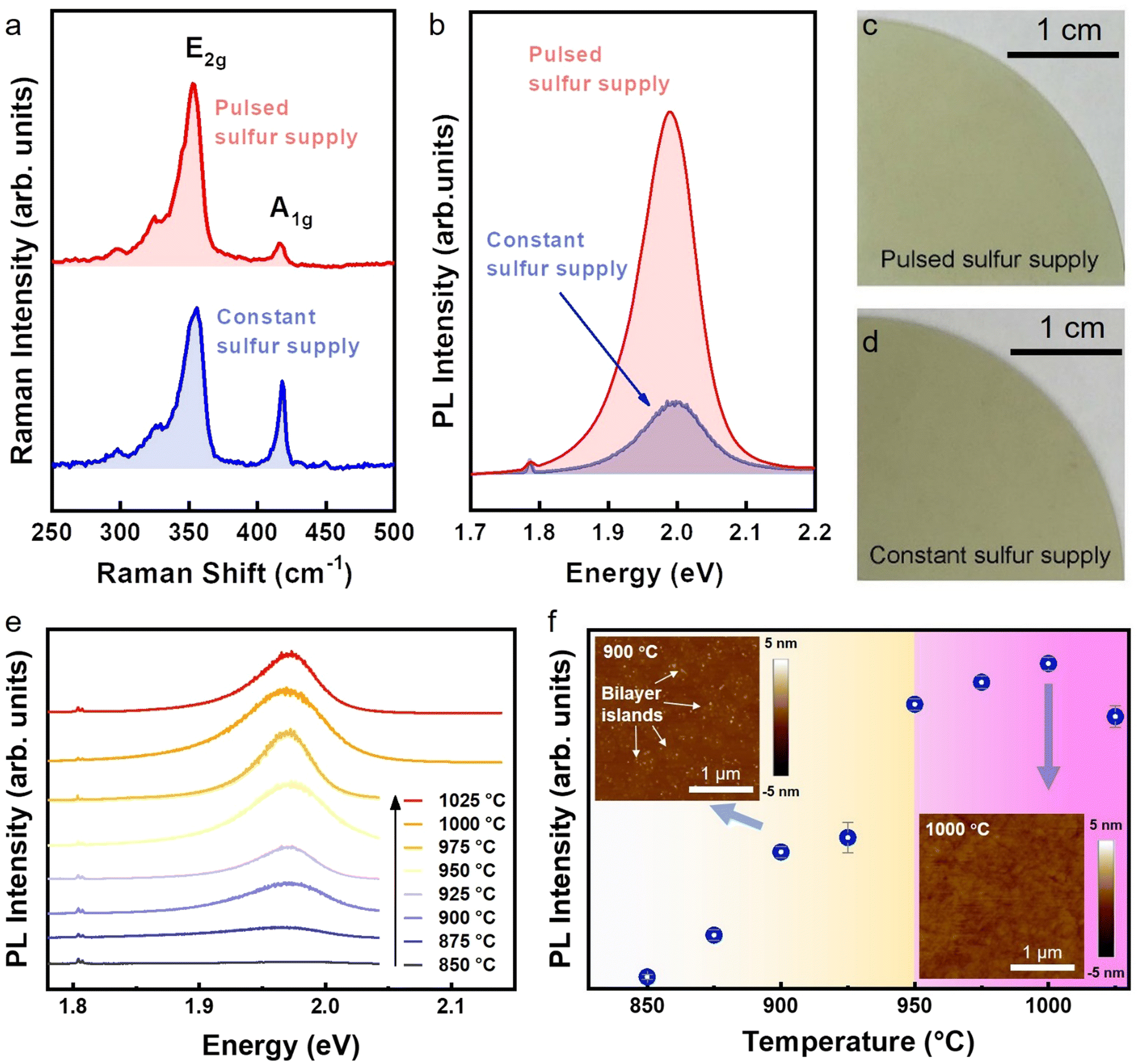 | ||
| Fig. 4 Structural characterization of PSS-WS2. (a) Raman feature, (b) PL spectrum and (c) photograph of PSS-WS2, compared with those measured on CSS-WS2. (e) PL spectra of PSS-WS2 prepared under various processing temperatures during the PSS process. (f) The intensities of the PL peaks as plotted in (e) with the error bars showing the standard mean. Insets are the AFM images of PSS-WS2 prepared under 900 °C and 1000 °C. The temperature-dependent optical/structural transition is highlighted into two colored zones. | ||
As opposed to the multilayer WS2 in the CSS-WS2 sample, the formation of monolayer PSS-WS2 certainly indicates that effective thinning of the multilayer WS2 occurs only during the DES turn-off periods. This is presumably due to the etching and/or enhanced sublimation of the top WS2 layers by H2. In understanding this thinning process, we note that there are several previous reports relevant to the thermal and chemical stability of WS2, which, together with our own experimental observations, may help to reveal the underlying mechanism. First, it was previously reported that a post-growth thermal treatment under H2 + Ar mixed gas is not effective in etching CVD-grown WS2 at temperatures up to 900 °C.24 This is in agreement with our experimental finding that monolayer WS2 formation by PSS is possible only for temperatures above 950 °C. As shown in Fig. 4e and f, there is a significant increase in the PL intensity of PSS-WS2 without the presence of bilayer domains upon preparing the film above 950 °C. This temperature-dependent optical/structural transition is highlighted into two colored zones showing that the multilayer WS2 and strictly-monolayer WS2 were prepared at low temperature range (850–925 °C) and high temperature range (950–1025 °C), respectively. This finding validates that a high enough temperature (larger than the vacuum sublimation temperature ∼870 °C of WS2)38 is crucial for providing the thermodynamic driving force to trim down the overgrown WS2 top layers from the bottom monolayer WS2/SAP. Second, a study of the thermal stability of WS2 and MoS2 in vacuum set the sublimation and decomposition temperatures for bulk WS2 around 870 °C and 1040 °C, respectively, as observed from the compact WS2 beginning to have a detectable weight loss rate at 870 °C and sulfur peaks appearing at 1040 °C.38 Third, Wu et al. demonstrated the vapor-solid growth of high optical quality MoS2 monolayers by the sublimation of the MoS2 powder source at 900 °C.39 Meanwhile, a vacuum sublimation temperature of ∼930 °C was determined for bulk MoS2, a temperature higher than the vacuum sublimation temperature ∼870 °C of bulk WS2.38
Based on the experimental observations summarized above and knowing the critical role of H2 in the PSS process (note: the formation of WS2 monolayer by PSS failed in the absence of H2 gas; see Fig. S6, ESI†), we explain the self-limited thinning of multilayer WS2 by PSS for the formation of a stable monolayer WS2 as follows. (1) At a temperature substantially higher than the vacuum sublimation temperature of ∼870 °C of WS2, there exists a certain thermodynamic driving force for multilayer WS2 to sublimate, with a drastically accelerated sublimation for highly volatile reduced WS2−x (Fig. 1j). (2) At a temperature (e.g., 1000 °C) much higher than ∼870 °C and in the presence of H2, the top few-layer WS2 (formed after the initial 600 °C sulfurization) would undergo a reduction process via H2(g) + WS2(s) → H2S(g) + WS2−x(s), leading to a drastically enhanced sublimation in the volatile WS2−x and thus layer-by-layer thinning, during DES turn-off periods (Fig. 1k). (3) This thinning process would be inhibited or drastically minimized in the presence of the DES supply (i.e., during DES turn-on period), due to the massive annihilation of S vacancies (created either during previous DES turn-off period or current DES turn-on period) by the readily available S atoms and, consequently, the restoration of the volatile WS2−x back to more stable WS2. During this DES turn-on period, further conversion of underlying remaining WOx, if there is any, into WS2 also takes place due to enhanced S diffusion through the top WS2 multilayer, the thickness of which was trimmed down during the previous turn-off period. (4) Once the multilayer WS2 finally reduces to a monolayer limit after several DES turn-on/turn-off cycles, the sublimation would stop effectively, even for the volatile WS2−x phase, most likely due to the stronger interface coupling of the bottom monolayer WS2 with sapphire substrate, as compared to that for WS2–WS2 interface. It should be noted that a more negative binding energy (Eb) of −2.23 eV is obtained for the monolayer WS2–sapphire interface as compared to Eb = −2.01 eV for the WS2–WS2 interface by DFT calculations (Fig. 3b), which means a significantly increased sublimation temperature for the monolayer WS2 on the sapphire surface. The effective suppression of sublimation in monolayer WS2 is also evident from the observation of the persistent existence of the PSS-WS2 monolayer after high temperature annealing under the steady flow of the H2 + Ar mixed gases without a DES supply (Fig. S7, ESI†). (5) The final pulse DES supply in a complete PSS process cycle would restore the WS2−x phase to a stable WS2 monolayer via a reaction of WS2−x(s) + xS(g) → WS2(s), thus realizing the self-limited thinning of multilayer WS2 for monolayer WS2 formation (Fig. 1l and m). (6) On the other hand, the failure in the formation of monolayer WS2 by the CSS process is due to the overwhelming restoration process (WS2−x(g) + xS(g) → WS2(s)) against the thinning process involving (1) reduction (H2(g) + WS2(s) → H2S(g) + WS2−x(s)) and (2) subsequent sublimation (WS2−x(s) → WS2−y(s) + volatile WS2−x(g)) under an environment with a constant sulfur supply. Here, we would like to highlight that the self-limited thinning process can also be employed on other suitable substrates, as demonstrated by the formation of the stable monolayer WS2 on SiO2/Si substrates (Fig. S8, ESI†). However, it is found that the formation of the monolayer MoS2 fails on SiO2/Si (i.e., complete stripping-off of MoS2), as shown in Fig. S9 (ESI†). In contrast, a continuous monolayer MoS2 is successfully prepared on sapphire substrates under the same PSS processing condition (Fig. S3, ESI†), clearly indicating the crucial effect of substrate on the PSS process and its extendibility. The instability of monolayer MoS2 on SiO2/Si is most likely due to the weaker binding energy of the MoS2–SiO2 interface than that for the MoS2–sapphire interface.
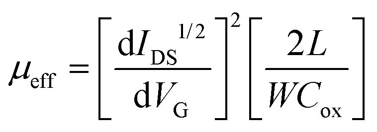
To investigate the electrical properties of the monolayer WS2 film grown via the self-limited thinning PSS process, bottom-gated FET devices were fabricated, with a channel length L = 25 μm and a channel width W = 200 μm, respectively. Fig. S10 (ESI†) shows the schematic of the device structure. Details of the device fabrication steps are described in the Methods. The fabricated WS2 FET devices exhibited typical n-channel FET characteristics, as shown in Fig. 5, similar to previous reports for WS2 FETs either with exfoliated or CVD-grown monolayer WS2 as a channel.13,40,41 The WS2 FET mobility was calculated using the expression,
 | (1) |
 | ||
| Fig. 5 Electrical characteristics of PSS-WS2 FETs. (a) Transfer characteristic curves at a fixed bias voltage of 2 V. (b) IDSversus VDS output curves at a step VGS from 0.4 to 2 V with 0.4 V intervals. | ||
Our values compare rather favorably to those reported in the literature (μeff = 0.16–1.97 cm2 V−1 s−1) for the exfoliated single crystalline monolayer WS2 FETs fabricated with similar source and drain metal contacts,9,42,43 implying the good quality of our monolayer WS2 film. It must be pointed out that, while the intrinsic mobility is a material-related parameter that is determined by intrinsic material properties such as crystallinity, crystal-defects/impurities, and grain sizes etc., μeff is also profoundly influenced by extrinsic effects, such as the contact resistance, gate-dielectric layer used, and integrity of the interface between the channel and gate-dielectric layer. For atomically-thin WS2 FETs, a μeff as high as 214 cm2 V−1 s−1 at 300 K was reported on single layer WS2 sandwiched between CVD-grown h-BN films.44 A μeff up to ∼115 cm2 V−1 s−1 at 300 K was also achieved for the exfoliated few-layer WS2 through monolayer-h-BN/Cr/Au tunneling barrier contact. In contrast, a low mobility of ∼1.44 cm2 V−1 s−1 at 300 K was extracted on the same few-layer WS2 film with direct Indium contact.42 Therefore, our reported carrier mobilities here should be taken as a lower limit of its intrinsic carrier mobility as there is still potential for improvement through various approaches, e.g., optimization of ALD oxide growth,45 choices of dielectric material (HfO2 instead of Al2O3),46 improvements in interface quality,44,47 while the contact resistance can also be further reduced.42,48 Nonetheless, our transport measurements indicate that a semiconducting WS2 monolayer film has been successfully grown uniformly by self-limited process on a 4 inch sapphire wafer.
Conclusions
In summary, a sublimation-based self-limited thinning process is demonstrated for the preparation of strictly monolayer WS2 on a 4-inch sapphire wafer. At a temperature substantially above the vacuum sublimation temperature of WS2, the multilayer WS2 formed by the sulfurization of the WOx precursor film is effectively trimmed down to the monolayer limit via the pulsed supply of sulfur precursor vapor under a continuous flow of H2. This self-limited thinning process is attributed to the following combined effect: (1) an effective reduction of stable WS2 to volatile reduced WSx phase by H2, and (2) significantly higher sublimation temperature of monolayer WS2 on sapphire as compared to multilayer or bulk WS2, as suggested by DFT calculations. The monolayer WS2 film showed high crystallinity and excellent property uniformity across the entire 4-inch wafer, as revealed by transmission electron microscopy (TEM), Raman microscopy, photoluminescence (PL), and X-ray photoelectron spectroscopy (XPS). The self-limited thinning process overcomes the intrinsic limitation of conventional vapor-based growth methods in preventing the 2nd layer WS2 domain nucleation/growth, and thus provides us with the strictly-monolayer WS2 on the wafer-scale. This approach opens a new avenue for a feasible manufacturing technology of 2D channel material for high efficiency optoelectronics.Methods
Sputtering growth of the WO3 precursor films
The WO3 were magnetron-sputtered on sapphire at a substrate temperature of 450 °C in pulsed DC mode using a W metal target. The base pressure of the system was 1.0 × 10⁻⁷ Torr. During the sputtering process, the working pressure was 2.6 × 10⁻³ Torr with Ar and O2 gas flow rates of 6 and 5 sccm, respectively. The pulsed DC power generator was operated at 5 kHz with reverse pulse widths of 0.4 μs. The thickness of WO3 is increased by increasing the sputtering time. For preparing WO3 with thicknesses of ∼1–3 nm, the sputtering duration was 12–30 s under the same power of 60 W.Formation and self-limited thinning process of multilayer WS2 for monolayer formation
For the growth of the WS2 monolayer, the wafer-sized sapphire substrates (c-plane, Namiki Precision Singapore Pte., Ltd) deposited with 1–3 nm WO3 precursor films were placed into a vertical 2-zone furnace. The chamber pressure was maintained at 10 Torr under the steady flow of mixed gases (78% volume Ar/22% volume H2). During the growth, 4 sccm diethyl sulfide (DES, (C2H5)2S, 98%, Sigma-Aldrich) was supplied from the bubbler at 30 °C and regulated precisely with a mass flow controller. Details of the pulsed supply of the DES and the process temperature temporal profile (600–1025 °C) are shown in Fig. 1b. Similarly, for the growth of the Co-doped WS2 monolayer, the substrate was firstly pre-deposited with a bilayer of Co (0.2 nm)/W (0.6 nm), and followed by the pulsed DES supply at 1000 °C. After the growth process, the quartz tube was naturally cooled down to room temperature under 200![[thin space (1/6-em)]](https://www.rsc.org/images/entities/char_2009.gif) sccm Ar gas.
sccm Ar gas.
Materials characterization
The morphologies of WS2 and Co-doped WS2 were analyzed via Bruker's dimension icon AFM system. The WITec alpha300S Raman instrument was used to measure the micro-Raman and photoluminescence (PL) spectra in order to confirm the quality and crystallinity of the grown WS2 and Co-doped WS2 film under a laser source with 532 nm wavelength. The XPS measurements for the pre-deposited tungsten oxides, WS2 and Co-doped WS2 were conducted by a VG ESCALAB 220i-XL system with a monochromatic Al Kα source and a pass energy of 10 eV. The optical absorption spectra were measured with the Shimadzu UV-VIS-NIR spectrophotometer UV-3150. To determine the atomic structure and orientations of the monolayer WS2, the FEI Titan 80/300 Scanning/TEM (200 kV) and FEI Tecnai F20 with fast Fourier transform (FFT) measurements were used for imaging the high-resolution TEM images after general transferring of the WS2 by poly(methyl methacrylate) (PMMA 950 in anisole, A5, KAYAKU Advanced Materials, Inc.) onto the 200-mesh TEM Cu grid. The focused ion beam (FIB) technique was employed to prepare a lamella, which was used for obtaining a cross-sectional image of the WS2 film.Simulation study
To execute the DFT simulations, the Vienna Ab initio Simulation Package (version 5.4) using the Perdew–Burke–Ernzerhof (PBE)49 was applied. The geometry was optimized under DFT simulation within the generalized gradient approximation.50,51 The expansion of the plane-wave had a kinetic energy cutoff at 450 eV. The slab structures consisted of Gamma-centered grids with 5 × 5 × 1 k-point grids were employed. Under the correction of the dipole and the DFT-D3 method,52 the interactions between the adjacent images and the dispersions were reduced respectively under the vacuum setting of no less than 14 Å.(2 × 2) Al2O3 and (3 × 3) WS2 were employed in building the model of WS2 on Al2O3. The lattice mismatch was smaller than 0.7% with around 9.3 Å thick Al2O3 slab. In the optimization stage, we have frozen the bottom four layers (total nine layers). The optimized lattices of the sapphire substrate (bulk Al2O3) were a = 4.785 Å and c = 13.053 Å, while the bulk WS2 (2H) were a = 3.169 Å and c = 12.423 Å. The oxygen-terminated slab models were constructed based on the bulk structures.
Considering the interaction along the interface will affect the thermal stability significantly, the theoretical binding energy (Eb) at the WS2–WS2 interface and WS2–sapphire interface (Fig. 3b) was calculated by eqn (2):
| Eb = Esubstrate+xWS2 − (Esubstrate+(x−1)WS2 + EWS2) | (2) |
Device fabrication and electrical measurements
SiO2/Si substrates and AlOx/p+-Si substrates were prepared by atomic layer deposition (ALD) method. A 30 nm of AlOx was grown by using 300 ALD cycles (Picosun) at 150 °C with the precursor trimethylaluminum (TMA) and oxidant H2O. Under a N2 carrier gas flow rate of 150 sccm, the pulse and purging time for TMA and H2O were set to 100 ms and 20 s, respectively, in every ALD cycle. The capacitance of AlOx was characterized by Keithley 4200. The 1 × 1 mm2 Au electrodes were evaporated onto AlOx to fabricate the metal–insulator–metal (MIM) capacitor device. Across the sweeping frequency range from 1000 to 106 Hz, Ci remains almost constant at ∼229 nF cm−2. Both SiO2/Si and AlOx/p+-Si substrates were cleaned by acetone and isopropanol (IPA) sequentially, and were subjected to 20 min O2 plasma (Harrick Plasma Cleaner) treatment to hydroxylate the oxide surface.To characterize the electrical performance, the monolayer WS2 was transferred onto the fresh target substrate by a conventional PMMA method.35 In short, PMMA was spun onto the as-grown WS2/sapphire with 3000 rpm for 60 s, and then heated at 150 °C for 2 min. Next, the PMMA-coated WS2 was separated from sapphire by dipping into 1 M KOH solution slowly. It was then picked up with a PDMS sheet, followed by rinsing in DI water several times to remove the residuals. Subsequently, the new PDMS stamp (DGL-45 × 45-0065-X4, GelPak) was then used to transfer the resultant film onto the target substrate and dried inside a fume hood overnight. Next, the PDMS was carefully detached from PMMA/WS2 at 150 °C, followed by a rinsing process to remove PMMA in the acetone and IPA baths. Finally, the sample was annealed at 300 °C for 30 min under Ar atmosphere.
The WS2 devices were fabricated based on the classical bottom-grid-top-electrode structure. The Ti/Au (10 nm/40 nm) electrodes were patterned by shadow mask under electron beam evaporation. The channel width and length were determined by Field Emission Scanning Electron Microscopy (FESEM, JEOL JSM7600F). Electrical measurements were carried out in air condition by a semiconductor device analyzer (B1500A, Agilent) equipped with probe stations (Probing Solutions, Inc.).
Author contributions
M. C.: writing – original draft. H. M and S. W. T: conceptualization. M. C., S. W. T., H. Z. and H. M. conducted the experiments including the growth and the transfer of WS2 for device fabrication and TEM study. J. C. conducted XPS measurements. M. C. and J. W. fabricated and characterized the two-terminal FETs. W. W. and M. L. performed the TEM measurements. J. L. and H. M. proposed and prepared the Co-doped WS2 samples. M.-F. N. performed and analyzed the DFT simulation results. S. W. T. and M. C. conducted the Raman, PL, AFM and UV-VIS measurements. J.-Y. K. and J. K. prepared the PVD sputtered MoS2. D. C., S. W. T., and H. M. supervised the work. All authors reviewed, edited, and approved the manuscript.Conflicts of interest
There are no conflicts to declare.Acknowledgements
The authors gratefully acknowledge financial supports from National Research Foundation Competitive Research Program (NRF-CRP24-2020-0002), the Institute of Materials Research and Engineering (IMRE) under the Agency for Science, Technology, and Research (A*STAR) via A*STAR Science and Engineering Research Council (SERC Grant No 152-70-00015, SERC Grant No A20G9b0135) and Career Development (Fund/C210112032). J. W. acknowledges the Advanced Manufacturing and Engineering Young Individual Research Grant (AME YIRG Grant No.: A2084c170) and the SERC Central Research Fund (CRF). We also acknowledge the National Supercomputing Centre (NSCC) Singapore and A*STAR Computational Resource Centre (A*CRC) of Singapore through the use of its high-performance computing facilities.References
- S. Das, A. Sebastian, E. Pop, C. J. McClellan, A. D. Franklin, T. Grasser, T. Knobloch, Y. Illarionov, A. V. Penumatcha, J. Appenzeller, Z. Chen, W. Zhu, I. Asselberghs, L.-J. Li, U. E. Avci, N. Bhat, T. D. Anthopoulos and R. Singh, Nat. Electron., 2021, 4, 786–799 CrossRef CAS.
- M. Chhowalla, D. Jena and H. Zhang, Nat. Rev. Mater., 2016, 1, 16052 CrossRef CAS.
- S. Manzeli, D. Ovchinnikov, D. Pasquier, O. V. Yazyev and A. Kis, Nat. Rev. Mater., 2017, 2, 17033 CrossRef CAS.
- C. Tan, X. Cao, X.-J. Wu, Q. He, J. Yang, X. Zhang, J. Chen, W. Zhao, S. Han, G.-H. Nam, M. Sindoro and H. Zhang, Chem. Rev., 2017, 117, 6225–6331 CrossRef CAS PubMed.
- K. F. Mak and J. Shan, Nat. Photonics, 2016, 10, 216–226 CrossRef CAS.
- C. S. Lau, J. Y. Chee, L. Cao, Z.-E. Ooi, S. W. Tong, M. Bosman, F. Bussolotti, T. Deng, G. Wu, S.-W. Yang, T. Wang, S. L. Teo, C. P. Y. Wong, J. W. Chai, L. Chen, Z. M. Zhang, K.-W. Ang, Y. S. Ang and K. E. J. Goh, Adv. Mater., 2021, 34, 2103907 CrossRef.
- Z. Huang, W. Zhang and W. Zhang, Materials, 2016, 9, 716 CrossRef.
- Y. Cui, R. Xin, Z. Yu, Y. Pan, Z.-Y. Ong, X. Wei, J. Wang, H. Nan, Z. Ni, Y. Wu, T. Chen, Y. Shi, B. Wang, G. Zhang, Y.-W. Zhang and X. Wang, Adv. Mater., 2015, 27, 5230–5234 CrossRef CAS.
- B. Tang, Z. G. Yu, L. Huang, J. Chai, S. L. Wong, J. Deng, W. Yang, H. Gong, S. Wang, K.-W. Ang, Y.-W. Zhang and D. Chi, ACS Nano, 2018, 12, 2506–2513 CrossRef CAS PubMed.
- K. Y. Ko, J.-G. Song, Y. Kim, T. Choi, S. Shin, C. W. Lee, K. Lee, J. Koo, H. Lee, J. Kim, T. Lee, J. Park and H. Kim, ACS Nano, 2016, 10, 9287–9296 CrossRef CAS.
- S. W. Tong, H. Medina, W. Liao, J. Wu, W. Wu, J. Chai, M. Yang, A. Abutaha, S. Wang, C. Zhu, K. Hippalgaonkar and D. Chi, ACS Appl. Mater. Interfaces, 2019, 11, 14239–14248 CrossRef CAS.
- P. Yang, L. Zhu, F. Zhou and Y. Zhang, Acc. Mater. Res., 2022, 3, 161–174 CrossRef CAS.
- J. Wang, X. Xu, T. Cheng, L. Gu, R. Qiao, Z. Liang, D. Ding, H. Hong, P. Zheng, Z. Zhang, Z. Zhang, S. Zhang, G. Cui, C. Chang, C. Huang, J. Qi, J. Liang, C. Liu, Y. Zuo, G. Xue, X. Fang, J. Tian, M. Wu, Y. Guo, Z. Yao, Q. Jiao, L. Liu, P. Gao, Q. Li, R. Yang, G. Zhang, Z. Tang, D. Yu, E. Wang, J. Lu, Y. Zhao, S. Wu, F. Ding and K. Liu, Nat. Nanotechnol., 2022, 17, 33–38 CrossRef CAS PubMed.
- H. Yu, M. Liao, W. Zhao, G. Liu, X. J. Zhou, Z. Wei, X. Xu, K. Liu, Z. Hu, K. Deng, S. Zhou, J.-A. Shi, L. Gu, C. Shen, T. Zhang, L. Du, L. Xie, J. Zhu, W. Chen, R. Yang, D. Shi and G. Zhang, ACS Nano, 2017, 11, 12001–12007 CrossRef CAS.
- T. Kim, J. Mun, H. Park, D. Joung, M. Diware, C. Won, J. Park, S.-H. Jeong and S.-W. Kang, Nanotechnology, 2017, 28, 18LT01 CrossRef.
- S. H. Choi, S. Boandoh, Y. H. Lee, J. S. Lee, J.-H. Park, S. M. Kim, W. Yang and K. K. Kim, ACS Appl. Mater. Interfaces, 2017, 9, 43021–43029 CrossRef CAS PubMed.
- Z. Lin, Y. Zhao, C. Zhou, R. Zhong, X. Wang, Y. H. Tsang and Y. Chai, Sci. Rep., 2015, 5, 18596 CrossRef CAS PubMed.
- X. Xu, T. Guo, H. Kim, M. K. Hota, R. S. Alsaadi, M. Lanza, X. Zhang and H. N. Alshareef, Adv. Mater., 2022, 34, 2108258 CrossRef CAS PubMed.
- K. Kang, S. Xie, L. Huang, Y. Han, P. Y. Huang, K. F. Mak, C.-J. Kim, D. Muller and J. Park, Nature, 2015, 520, 656–660 CrossRef CAS PubMed.
- X. Li, W. Cai, J. An, S. Kim, J. Nah, D. Yang, R. Piner, A. Velamakanni, I. Jung, E. Tutuc, S. K. Banerjee, L. Colombo and R. S. Ruoff, Science, 2009, 324, 1312–1314 CrossRef CAS PubMed.
- S. H. Choi, H.-J. Kim, B. Song, Y. I. Kim, G. Han, H. T. T. Nguyen, H. Ko, S. Boandoh, J. H. Choi, C. S. Oh, H. J. Cho, J. W. Jin, Y. S. Won, B. H. Lee, S. J. Yun, B. G. Shin, H. Y. Jeong, Y.-M. Kim, Y.-K. Han, Y. H. Lee, S. M. Kim and K. K. Kim, Adv. Mater., 2021, 33, 2006601 CrossRef CAS PubMed.
- I. Bilgin, F. Liu, A. Vargas, A. Winchester, M. K. L. Man, M. Upmanyu, K. M. Dani, G. Gupta, S. Talapatra, A. D. Mohite and S. Kar, ACS Nano, 2015, 9, 8822–8832 CrossRef CAS PubMed.
- C. M. Schaefer, J. M. Caicedo Roque, G. Sauthier, J. Bousquet, C. Hébert, J. R. Sperling, A. Pérez-Tomás, J. Santiso, E. del Corro and J. A. Garrido, Chem. Mater., 2021, 33, 4474–4487 CrossRef CAS.
- Y. Zhang, Y. Zhang, Q. Ji, J. Ju, H. Yuan, J. Shi, T. Gao, D. Ma, M. Liu, Y. Chen, X. Song, H. Y. Hwang, Y. Cui and Z. Liu, ACS Nano, 2013, 7, 8963–8971 CrossRef CAS PubMed.
- Y. Shi, B. Groven, Q. Smets, S. Sutar, S. Banerjee, H. Medina, X. Wu, C. Huyghebaert, S. Brems, D. Lin, P. Morin, M. Caymax, I. Asselberghs and I. Radu, 2021 IEEE International Electron Devices Meeting (IEDM), 2021, 37.1.1–37.1.4 Search PubMed.
- Q. Smets, G. Arutchelvan, J. Jussot, D. Verreck, I. Asselberghs, A. N. Mehta, A. Gaur, D. Lin, S. E. Kazzi, B. Groven, M. Caymax and I. Radu, 2019 IEEE International Electron Devices Meeting (IEDM), 2019, 23.2.1–23.2.4 Search PubMed.
- T. Li, W. Guo, L. Ma, W. Li, Z. Yu, Z. Han, S. Gao, L. Liu, D. Fan, Z. Wang, Y. Yang, W. Lin, Z. Luo, X. Chen, N. Dai, X. Tu, D. Pan, Y. Yao, P. Wang, Y. Nie, J. Wang, Y. Shi and X. Wang, Nat. Nanotechnol., 2021, 16, 1201–1207 CrossRef CAS.
- H. Zhu, X. Qin, L. Cheng, A. Azcatl, J. Kim and R. M. Wallace, ACS Appl. Mater. Interfaces, 2016, 8, 19119–19126 CrossRef CAS.
- S. Kim, M. S. Choi, D. Qu, C. H. Ra, X. Liu, M. Kim, Y. J. Song and W. J. Yoo, 2D Mater., 2016, 3, 035002 CrossRef.
- M. A. Bissett, A. G. Hattle, A. J. Marsden, I. A. Kinloch and R. A. W. Dryfe, ACS Omega, 2017, 2, 738–745 CrossRef CAS PubMed.
- Y. Huang, J. Wu, X. Xu, Y. Ho, G. Ni, Q. Zou, G. K. W. Koon, W. Zhao, A. H. Castro Neto, G. Eda, C. Shen and B. Özyilmaz, Nano Res., 2013, 6, 200–207 CrossRef CAS.
- M. Chhowalla, H. S. Shin, G. Eda, L.-J. Li, K. P. Loh and H. Zhang, Nat. Chem., 2013, 5, 263–275 CrossRef.
- Y. Lee, J. W. Jung and J. S. Lee, Mater. Chem. Front., 2021, 5, 3692–3698 RSC.
- T. H. Choudhury, H. Simchi, R. Boichot, M. Chubarov, S. E. Mohney and J. M. Redwing, Cryst. Growth Des., 2018, 18, 4357–4364 CrossRef CAS.
- Y.-C. Shen, Y.-T. Wu, L. Lee, J.-H. Chen, S. S. Wani, T.-Y. Yang, C. W. Luo, M.-D. Siao, Y.-J. Yu, P.-W. Chiu and Y.-L. Chueh, Adv. Funct. Mater., 2021, 31, 2104978 CrossRef CAS.
- S. J. Yun, S. H. Chae, H. Kim, J. C. Park, J.-H. Park, G. H. Han, J. S. Lee, S. M. Kim, H. M. Oh, J. Seok, M. S. Jeong, K. K. Kim and Y. H. Lee, ACS Nano, 2015, 9, 5510–5519 CrossRef CAS.
- W. Zhao, Z. Ghorannevis, K. Kumar Amara, J. R. Pang, M. Toh, X. Zhang, C. Kloc, P. H. Tane and G. Eda, Nanoscale, 2013, 5, 9677–9683 RSC.
- W. A. Brainard, The thermal stability and friction of the disulfides, diselenides, and ditellurides of molybdenum and tungsten in vacuum (10−9 to 10−6 Torr), National Aeronautics and Space Administration; Springfield, Va., Washington, DC, 1968 Search PubMed.
- S. Wu, C. Huang, G. Aivazian, J. S. Ross, D. H. Cobden and X. Xu, ACS Nano, 2013, 7, 2768–2772 CrossRef CAS PubMed.
- D. Ovchinnikov, A. Allain, Y.-S. Huang, D. Dumcenco and A. Kis, ACS Nano, 2014, 8, 8174–8181 CrossRef CAS PubMed.
- A. Sebastian, R. Pendurthi, T. H. Choudhury, J. M. Redwing and S. Das, Nat. Commun., 2021, 12, 693 CrossRef CAS PubMed.
- N. A. N. Phan, H. Noh, J. Kim, Y. Kim, H. Kim, D. Whang, N. Aoki, K. Watanabe, T. Taniguchi and G.-H. Kim, Small, 2022, 18, 2105753 CrossRef CAS PubMed.
- D. H. Jung, G. H. Oh, S. Kim and T. W. Kim, Jpn. J. Appl. Phys., 2022, 61, 034001 CrossRef.
- M. W. Iqbal, M. Z. Iqbal, M. F. Khan, M. A. Shehzad, Y. Seo, J. H. Park, C. Hwang and J. Eom, Sci. Rep., 2015, 5, 10699 CrossRef CAS.
- J.-G. Song, S. J. Kim, W. J. Woo, Y. Kim, I.-K. Oh, G. H. Ryu, Z. Lee, J. H. Lim, J. Park and H. Kim, ACS Appl. Mater. Interfaces, 2016, 8, 28130–28135 CrossRef CAS PubMed.
- B. Radisavljevic, A. Radenovic, J. Brivio, V. Giacometti and A. Kis, Nat. Nanotechnol., 2011, 6, 147–150 CrossRef CAS PubMed.
- Y. J. Kim, W. Park, J. H. Yang, Y. Kim and B. H. Lee, IEEE J. Electron. Dev., 2018, 6, 164–168 CAS.
- P.-C. Shen, C. Su, Y. Lin, A.-S. Chou, C.-C. Cheng, J.-H. Park, M.-H. Chiu, A.-Y. Lu, H.-L. Tang, M. M. Tavakoli, G. Pitner, X. Ji, Z. Cai, N. Mao, J. Wang, V. Tung, J. Li, J. Bokor, A. Zettl, C.-I. Wu, T. Palacios, L.-J. Li and J. Kong, Nature, 2021, 593, 211–217 CrossRef CAS PubMed.
- J. P. Perdew, K. Burke and M. Ernzerhof, Phys. Rev. Lett., 1996, 77, 3865–3868 CrossRef CAS.
- G. Kresse and J. Furthmüller, Phys. Rev. B: Condens. Matter Mater. Phys., 1996, 54, 11169–11186 CrossRef CAS.
- P. E. Blöchl, Phys. Rev. B: Condens. Matter Mater. Phys., 1994, 50, 17953–17979 CrossRef.
- S. Grimme, J. Antony, S. Ehrlich and H. Krieg, J. Chem. Phys., 2010, 132, 154104 CrossRef.
Footnote |
| † Electronic supplementary information (ESI) available. See DOI: https://doi.org/10.1039/d3nh00358b |
| This journal is © The Royal Society of Chemistry 2024 |