
 Open Access Article
 This Open Access Article is licensed under a Creative Commons Attribution-Non Commercial 3.0 Unported Licence
Universal skyrmion logic gates and circuits based on antiferromagnetically coupled skyrmions without a topological Hall effect†
Rawana
Yagan
 *a,
Arash Mousavi
Cheghabouri
a and
Mehmet C.
Onbasli
*ab
*a,
Arash Mousavi
Cheghabouri
a and
Mehmet C.
Onbasli
*ab
aDepartment of Electrical and Electronics Engineering, Koç University, Sarıyer, Istanbul 34450, Turkey. E-mail: ryagan18@ku.edu.tr; monbasli@ku.edu.tr
bDepartment of Physics, Koç University, Sarıyer, Istanbul 34450, Turkey
First published on 2nd November 2024
Abstract
Nanoscale skyrmions are spin-based quasiparticles that are promising for nonvolatile logic applications. However, the presence of the skyrmion Hall effect (SkHE) in ferromagnetic skyrmions limits their performance in logic devices. Here, we present a detailed micromagnetic modeling study on low-energy skyrmion logic gate circuits based on skyrmions in synthetic antiferromagnetically coupled (SAF) metallic ferromagnetic layers to eliminate the SkHE while reducing current requirements. First, we demonstrate the functionalities of the SAF skyrmion logic inverter gate and other Boolean gates such as NOR, OR, AND, and NAND using the inverter gate block and show the improved performance over their ferromagnetic skyrmion gate counterparts. We analyzed the operation and energy consumption at different stages of the SAF skyrmion logic operation and found that the SAF gates can operate at lower current densities. We designed a multiplexer circuit as a test case and obtained a fast response and low Joule heating. The skyrmion motion through the gates is shown to be stable and efficient in different regions, and cascading the gates creates longer linear motion without the unwanted transverse SkHE. Overall, the results indicate the feasibility of antiferromagnetically coupled skyrmions for low-energy logic with improved performance over ferromagnetic skyrmionics.
Introduction
Skyrmion-based devices have shown promise in achieving fast response, non-volatile, ultra-low power logic, and memory systems. Topologically protected skyrmions are nanoscale spin-based quasiparticles that can be moved, generated, and destroyed using a current or magnetic field. These make them advantageous building blocks for logic and data storage applications1 and neuromorphic computing.2 Current-induced motion is one of the promising approaches for moving skyrmions through ferromagnetic materials and in racetrack memories3,4via spin-transfer torques (STTs), which result from applying spin-polarized currents.5–8 Previous studies used FM skyrmions to investigate magnetic skyrmion-based devices with high speeds and minimal energy consumption.9–11 Although shown to offer high velocities in theory, the presence of the topological Hall effect or the skyrmion Hall effect (SkHE),12,13 limits the FM skyrmion performance and its velocity when driven by current pulses in racetracks in memory or logic devices. For information processing, the current-driven transverse motion of skyrmions in a nano track is called SkHE, and this effect prevents the lateral movement of skyrmions during subsequent logic gate operations. Thus, to design any skyrmion-based digital logic device application and use the merits of skyrmions for logic applications, SkHE must be eliminated by establishing an appropriate balance for forces or torques acting on a current-driven skyrmion.Previous research relied on tweaking the STT-driven motion in their micromagnetic models by balancing the field-like and damping-like torque perfectors to drive FM skyrmion in a lateral trajectory with no transverse displacement.14,15 Others studied theoretical models of enhancing the material properties of the boundary of the track at the edges16–18 or by creating track-assisted walls19 and predefined skyrmion to track with ratios20 to prevent the skyrmion from being destroyed at the track edges. However, realistically, FM skyrmions suffer from instability in linear nanotracks that causes loss of information,21 requiring the realization of the design of such structures with higher complexity of logic and memory devices. The challenge of identifying magnetic thin films and multilayer structures that can host stable skyrmions and can be manipulated by electrical currents at room temperatures with low densities has been identified as a key issue in skyrmion-based logic devices. In addition, issues still lie ahead in balancing the trade-off between low energy consumption and high switching speed in gate processing and providing skyrmion with lower radii to downscale these skyrmion devices for higher information density.
Previously, we showed using micromagnetic models that FM skyrmion logic gates and circuits can be designed using current-driven geometries that use domain walls to gate skyrmion motion.6,22 In that study, we used mirror symmetry breaking of vertical in-plane tracks to convert incoming logic skyrmion bits into domain walls, which act as gatekeepers against probing skyrmions. These probing skyrmions essentially act as clock signals regarding microelectronic circuit design. Those circuits could shrink logic operations significantly into nanometer-square areas. Still, one major shortcoming is the skyrmion Hall effect or topological Hall effect, which is the in-plane transverse deflection of skyrmions due to Magnus force while being current-driven along in-plane longitudinal direction. This shortcoming may prevent cascadable circuits that carry out larger-scale logic operations. Thus, the Magnus force must be compensated to ensure that skyrmions do not deflect for a broad window of material, geometry, and external drive parameters.20,23 Antiferromagnetic24 and ferrimagnetic23 materials possess such properties. However, few experimental observations of skyrmions at room temperature have been reported.
To solve the skyrmion Hall effect problem, synthetic antiferromagnetically coupled (SAF) ferromagnetic multilayers might help minimize the Magnus force. Skyrmions are stabilized in SAF ferromagnetic multilayers both theoretically25,26 and experimentally.27,28 These quasiparticles offer enhanced static stability and improved dynamic motion characteristics compared to skyrmions in FM-based devices with the absence of SkHE. These skyrmions can provide guided motion due to the absence of the Magnus force fundamentally present in FM skyrmion longitudinal tracks. In the SAF layers, we modeled in ref. 25, FM skyrmion pair existing with opposite topological charge signs in top and bottom interfaces couple antiferromagnetically through the Ruderman–Kittel–Kasuya–Yosida (RKKY) interlayer exchange interaction29 that is mediated via the sandwiched non-magnetic (NM) spacer layer.
Due to the strong coupling of skyrmions along the two interfaces, SAF multilayers provide current-driven stability to the skyrmion pair in such a way as to improve its velocity and establish an adiabatic drive while using lower current densities.25 These models show that stable skyrmions can be driven at current densities several orders of magnitude lower than those required by FM skyrmions to reach velocities in a couple of hundred m s−1. External fields have been found to affect the coupling strength between SAF skyrmion pairs. This achievement enables the design of SAF skyrmion logic devices with low energy consumption, low drive current densities, high skyrmion velocity, and no transverse displacements.
Very few models on SAF skyrmion-based devices30–32 have been shown previously to perform any logic operations. Hence, we highlight the need to investigate the performance and switching time of such promising systems in SAF configuration and under external bias conditions for functional logic gates and circuits. Based on our previous study conducted on skyrmions in SAF multilayers and comparing with the existing FM skyrmion and DW systems, five distinct features of SAF skyrmions in racetrack memory and logic devices emerge: (i) with the absence of the SkHE, SAF skyrmions can move along the spin-polarized current direction in a straight line. (ii) As the net magnetization of skyrmion is zero, it can endure magnetic perturbations with considerable robustness. (iii) Spin currents can push SAF skyrmions at greater velocities than FM skyrmions and the domain walls27 with up to 3 orders of magnitude lower current densities, further reducing the Joule heating effects. (iv) SAF-skyrmion-based logic gates can simplify the driving mode of devices, reduce energy consumption, increase the speed of skyrmion motion, and expand the variety of logic functions. (v) They show thermal stability, strong coupling against external magnetic fields, and large current densities due to the strong AFM coupling in the RKKY constant Jint.25,27,33–36
In this study, we use micromagnetic models and the merits of SAF skyrmions to design SAF logic gate devices and circuits that could be cascaded for the feasible operation of arbitrarily large circuits and Boolean operations. We focus our investigation in this paper on the features of SAF skyrmions in logic applications and provide a model based on SAF multilayers25 for FM skyrmion logic gates from the micromagnetic model of the logic inverter gate for the [Co/Pt] bilayer6 and redesign the FM micromagnetic continuum model to present the case of the skyrmion pair in SAF multilayers. The MuMax3 and post-processing scripts are published as a GitHub repository under the project name “SAF-Logic”.37
The operation of many skyrmion-based logic devices consists of skyrmion generation, initialization, skyrmion-based transfer, manipulation techniques, and final output reading and processing. Skyrmions can be generated using local spin-polarized current pulses injection,38–40 magnetic fields,41 optical pulses,42 and current-assisted generation through nanoscale constrictions.43–45 Most of the processes involved in these logic gates and computational structures are based on the skyrmions alone as information carriers4,46 or the dynamics of skyrmions and DW in nanotracks.5,45 Some of these processes concerning the latter method include the reversible conversion and the collision between the skyrmion and the domain wall,14,47 skyrmion–skyrmion, and skyrmion–edge repulsion.48 In this paper, we will adapt the FM skyrmion-based logic blocks presented in the previous work in ref. 6 and in ref. 22 into the SAF skyrmion system based on the domain wall-gated skyrmion logic.47,49 These models show an all-skyrmion inverter logic that demonstrates the capability for asynchronous, low nanosecond delay, thermally robust, low-power, high-bandwidth, and scalable systems as compared to other methods such as voltage-gated logic46,50 and skyrmion–skyrmion logic.51
In the following sections, we present simulation models and the SAF skyrmion logic inverter gate operation by describing the different physics and interactions involved, which show that it offers better performance characteristics than the FM skyrmion case. We study the performance parameters of these SAF skyrmionic gates in terms of velocity response to applied current density J and output delivery within the desired application time with minimum latencies. Using current-driven skyrmion motion via spin–orbit torques, skyrmion edge repulsion, skyrmion–DW pair conversion, and collision in the SAF multilayer structure, we show the operation of the SAF skyrmion logic inverter block. We then implement and expand the functionality of the inverter gate to construct logic OR, NOR, AND, and NAND operations using the inverter block as the basic element constituting these gates. These Boolean operations are demonstrated for skyrmion-based input and probe signals that allow for the desired output by cascading and rotating the inverter blocks. As a demonstration, we show the design and operation of an SAF skyrmion-based digital multiplexer circuit. We aim to show that SAF-based skyrmion logic can pave the way for realizing such logic gate designs with minimum power consumption, improved response, and higher switching speeds.
Micromagnetic model of SAF logic gates
SAF multilayers and heterostructures have been proposed to improve skyrmion stability and mobility by eliminating the SkHE. In this paper, we show and evaluate the functionality of the SAF skyrmion-based logic gates using micromagnetic modeling adapted from ref. 6 and 14 for the FM-based skyrmion logic and computational gates. Source codes, videos, and sample data of the different logic gates and circuits are available at the GitHub link.37The structure shown in Fig. 1(a) is the simulated inverter gate in MuMax3 micromagnetic solver,52 where the magnetization dynamics are controlled by the modified Landau–Lifshitz–Gilbert (LLG) equation with the additional spin–orbit torque (SOT) term (see equation in ESI S1†), that includes the applied current density (J). The dimensions of the inverter gate are provided in ESI Fig. S1,† where the mesh size is set to 1 × 1 × 1 nm3. The material parameters used in the simulations for SAF multilayers (FM/NM/FM) are adopted from the (W/Co/CoFeB/Ir/Co/CoFeB/Pt) SAF coupled multilayers through the Ir spacer layer in ref. 27 for each 1 nm FM layer. They are as follows: saturation magnetization (Msat) = 954 × 103 A m−1, interfacial Dzyaloshinskii–Moriya constant (Dind) = 2.0 × 10⁻³ J m−2, uniaxial anisotropy constant (Ku) = 0.85 × 10⁶ J m−3, along the z-direction, Heisenberg exchange (A) = 10 × 10−12 J m−1, and Gilbert damping (α) = 0.1. In ref. 25 a detailed study of the stability and dynamic response of the SAF skyrmion pair showed that these skyrmions can be driven by SOT current densities with greater stability and improved linear velocity. This is due to the absence of the Magnus force (total topological charge equal to zero), eliminating the SkHE present in FM skyrmion long nanowires. The spin-Hall angle is 0.25, and the SOT parameter pair (χ, λ) is (−2, 1). The large spin Hall angle for the SAF multilayers allows for utilizing low current densities applied through the SOT method (current perpendicular to the plane method described in ESI S1†). The interlayer exchange coupling between the top and bottom skyrmions mediated through the Ir layer (see schematic Fig. 1(a)) is governed by the antiferromagnetic (AFM) exchange constant Jint = −0.26 × 10⁻³ J m−2. This antiferromagnetic coupling is known as the RKKY interaction, electronically mediated through the spacer (NM) layer.53
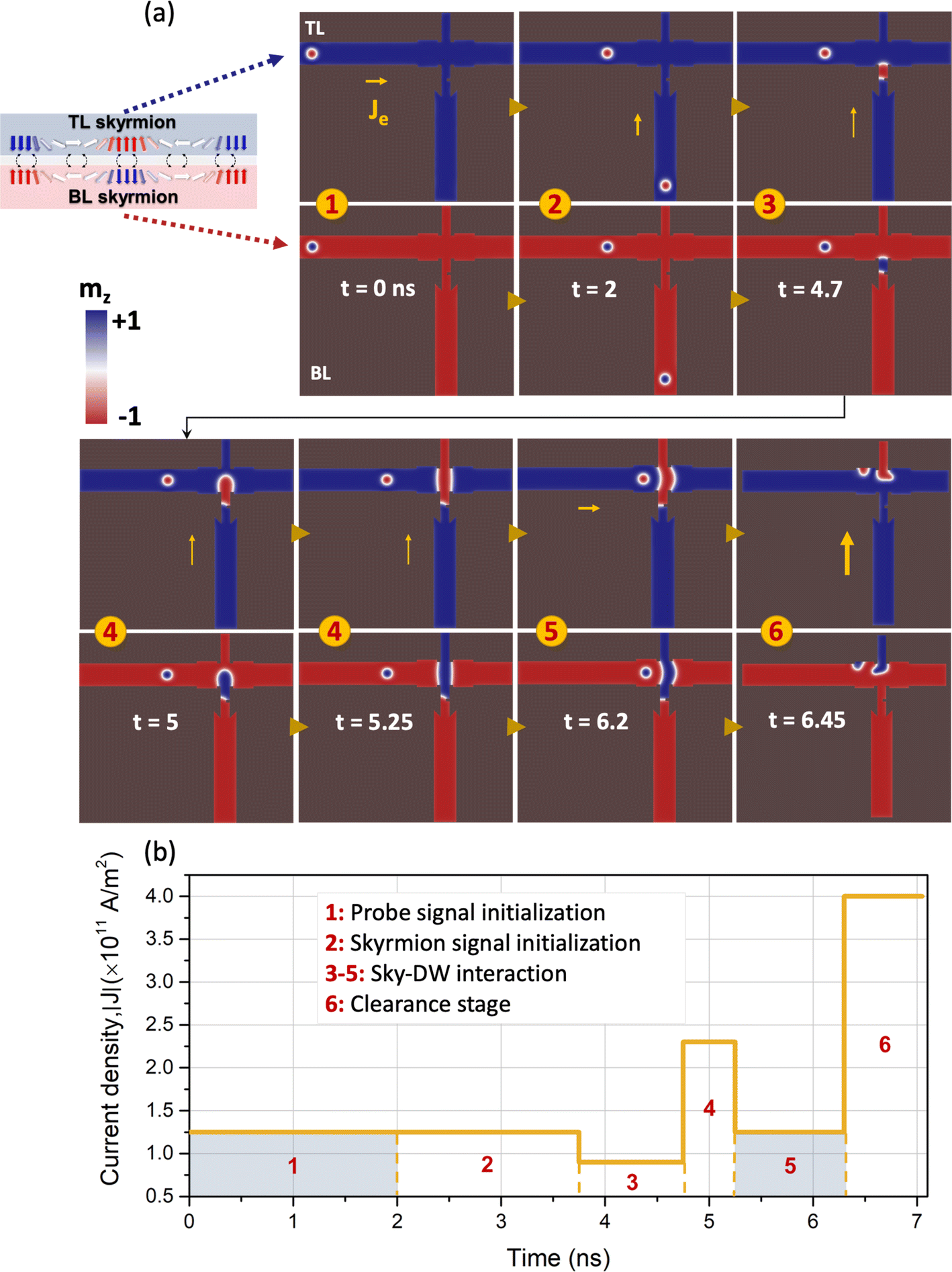 | ||
| Fig. 1 Inverter gate operation in the SAF system. (a) The different stages shown for SAF paired skyrmions are shown with the top layer (TL) showing the skyrmion of core orientation −z and the bottom layer (BL) showing the skyrmion of +z core. The yellow arrows resemble the resulting current density (Je) direction and magnitude from the applied J to the gate channels. (b) The applied current density time plot is based on the different stages of gate operation. In stages 1 and 5, the current is applied in the +x direction, while in the other stages, the Je is applied in +y. | ||
We used a larger value for the coefficient Jint than the one used in ref. 25 to make sure that the coupling between the SAF skyrmion pairs is strong enough to withstand the deliberately induced geometrical effects and the track width changes along the traveled path of the SAF skyrmion, which increases the energy barrier imposed on the AFM coupled skyrmions. The SOT current was applied to the inverter gate's horizontal and vertical channels in a current perpendicular-to-plane (CPP) configuration. The current densities were modified in accordance with the timed plots in Fig. 1(b) when the skyrmion/DW pair approached the different stages in its path. In the region where demagnetizing fields were sufficient to form an energy barrier that prevented these magnetic features from traveling in the direction of the applied spin current, these current levels were increased.
Prior to executing the gate operation in the simulation, SAF skyrmion pairs (each of which is of the Néel type, with cores magnetized in opposition to one another) were formed on the layer interfaces and relaxed in the constructed geometry for both gates. The skyrmion and DW pair conversion occurs for both interfaces across the gate layers. This conversion demonstrates that the DW pair and the skyrmion have a Néel configuration. Within the SAF bilayer, we demonstrate that the skyrmion pair can traverse the inverter gate channels at high velocities when driven by spin current density (J). This characteristic proves beneficial in simplifying the operation of devices based on skyrmion technology. The logic gates examined in this study are operated by the utilization of current-driven skyrmion motion within restricted geometries, DW pair pinning and expansion, and interaction between skyrmion–DW pairs. In the subsequent section, we will examine the operation and performance of the SAF Skyrmion Inverter, as well as the cascaded AND, NAND, OR, and NOR gates, and digital multiplexer circuit.
Inverter block (basic building block)
In the inverter block scheme depicted in Fig. 1, two distinct types of skyrmion signals are utilized: probing and input signals. In stage 1, the SAF skyrmion is first created and then driven by applying J = 1.25 × 10¹¹ A m−2 in the horizontal channel for 2 ns. The input signal skyrmion is initialized in stage 2 in this process as the signal bit 1 and is transferred through the vertical channel until it reaches the narrow channel. During stage 3, applying the previous high current value will cause the skyrmion pair to decouple and lose its stability as it enters the narrow channel. Therefore, in this step, we decrease J to 0.9 × 10¹¹ A m−2 to facilitate a smooth transition from the SAF skyrmion state to the SAF coupled DW pair and to ensure the second DW is securely pinned. In stage 3, the first DW moves through the recessed notch region with a reduced energy barrier, while the second wall gets pinned. Due to the low current applied, the DW expands through the narrow channel but cannot exit and pass through the crossed region in stage 4. The initial DW retracts to its original shape, forming a straight wall in stage 4 with a lower energy state. Applying a higher current density (2.25 × 10¹¹ A m−2) in the vertical channel causes the DW to shift and expands the domain until it reaches the end of the channel. Applying J to the horizontal channel brings the SAF skyrmion closer to the left DW, effectively hindering the skyrmion movement within the channel. This is classified as output logic 0, as observed in stage 5. The clearance stage 6 ensures that the gate is completely cleared by applying an intense current in the vertical channel and the two side notches, which can reduce the protected topology and eliminate all the magnetic features present. The energy consumption of the inverter device as a function of time is shown in ESI Fig. S4.† The operation stages of the inverter block are demonstrated in ESI Video SV1.†Through a comparison of the performance of the SAF skyrmion inverter gate to the FM case (refer to ref. 6), several observations can be made. We can specifically compare the logic switching delay (td) of the SAF and FM skyrmion gates. This performance metric is determined by the velocity of skyrmions and the distance between input and output terminals.31,54 The SAF skyrmion gate demonstrates a similar response time to the FM skyrmion gate but operates at significantly lower current densities. This advantage enables operation with reduced Joule heating costs while maintaining a fast response, with td of approximately 7 ns. Therefore, the SAF skyrmion and DW pair maintain their stability, integrity, and fast response without interference from the Magnus force effects or any unwanted transverse deflections caused by their interaction.
The demagnetization field spatial distribution is shown in Fig. 2, where we observe that the field distribution changes when the probing SAF skyrmion approaches the narrow channel and when the signal skyrmion collides with the DW.
 | ||
| Fig. 2 Demagnetization field (Bdemag) spatial distribution at the different stages of the inverter gate operation is shown for the bottom interface. One layer in the SAF provides the mirrored response of the other. | ||
Consequently, we analyze the time evolution of the total and demagnetization energies, Etotal and Edemag, respectively, of the logic gate depicted in Fig. 2. When current J is applied to the multilayers, an oscillatory behavior in Edemag and a peak response in Etotal can be observed. Overcoming the energy barriers by applying a suitable amount of J allows us to push them through the channels, notches, and edge effects. During stages 3 and 4, as the DW pair moves through the vertical channel, there is an energy barrier that the first DW encounters at the intersection. This leads to an increase in Edemag as the DW bends and retracts. At this stage, the total energy decreases due to the influence of competing forces, such as the Heisenberg exchange and magnetostatic energies. As the skyrmion moves towards the left DW, Edemag decreases because of the growing repulsion forces between these objects, causing Etotal to increase in response to the induced anisotropy changes. The total energy consumption of the SAF skyrmion inverter gate is calculated to be 2.17 × 10⁻¹⁸ J. This calculation is based on taking the derivative of Etotal, giving the instantaneous power due to the contributions of the different energy terms driving the SAF skyrmion pair through the channels, and then integrating the positive region of the instantaneous power vs. time data (Fig. 3).6
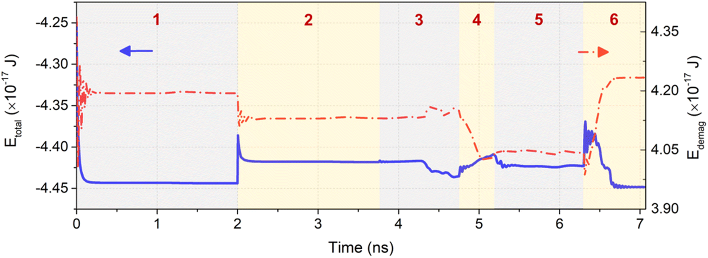 | ||
| Fig. 3 SAF skyrmion inverter gate energy response plot shows the total energy (Etotal) and demagnetizing energy (Edemag) time response during the gate operation. | ||
SAF skyrmion logic gates
Constructing Boolean logic gates from the inverter block can be achieved by cascading and connecting these basic blocks, and by rotating the block, we control the transition of the input skyrmion to yield the desired logic output. The concept of creating these logic circuits from the inverter (NOT) gate is demonstrated and described in ref. 22. In Fig. 4(a) and (b), the NOR and OR gates are shown for two cases of logic inputs (0, 0) and (1, 0). The OR gate in Fig. 4(b) is extended from the NOR gate by connecting an inverter block's vertical channel to the output of the NOR gate. In this case, the final inverter block is rotated by +90°. The switching time (td) of the SAF NOR gate is 9.3 ns, and an additional 4.55 ns is used to obtain the output of the OR gate. In the NOR (0, 0) operation, there are no input skyrmions from the two bottom vertical channels, which leads the probing skyrmion to pass through the main horizontal channel without any constriction all the way to the output region, representing logic 1. As for the NOR (1, 0) operation, the existence of an input skyrmion at the first vertical channel will block the way of the probing skyrmion through the skyrmion–DW encounter. Thus, a logic 0 is yielded with the absence of skyrmion in the output region. The simulation results for the time evolution of the NOR gate operation are shown in ESI Videos SV2–SV4.† In Fig. 4(b), we demonstrate the logic (0, 0) and (1, 0) operation of the OR gate. In this case, and compared to the NOR gate operation, the presence of the third cascaded inverter gate would count for the logic complement operation. The probing skyrmion traveling through the main horizontal channel would prevent another probing skyrmion coming from the third vertical channel from traveling to the output region, thus obtaining a logic 0 for this specific operation. We map the same process for the case of inputs (1, 0) and the output 1 for the OR gate, where the last horizontal channel skyrmion travels to the output region. The simulation results for the time evolution of the OR gate operation are shown in ESI Videos SV5 and SV6.† | ||
| Fig. 4 Logic (a) NOR gate, of inputs (0, 0) and (1, 0), and (b) OR gate, of inputs (0, 0) and (1, 0), constructed from the inverter blocks showing the different stages of the SAF skyrmion input signals and probing skyrmions of the top and bottom layers transitions which lead to the output logic of the respective gates (BL: bottom layer, TL: top layer). | ||
Fig. 5 shows examples of logic operations AND and NAND for the SAF skyrmion system. In the case of the AND gate construction, the first inverter block (from the left) is mirror-flipped off the horizontal axis, and the input skyrmion would travel in the top vertical channel. In the AND (0, 1) case, since there is no input 1 skyrmion, the probing skyrmion would travel the main horizontal channel all the way to the junction, converting to DW pair and blocking the 2nd input skyrmion, achieving the logic 0 result. While, in the AND (1, 1) case, the input 1 skyrmion would block the probing skyrmion allowing the input 2 skyrmion to travel down to the output region, with output logic 1. The simulation results for the time evolution of the AND gate operation are shown in ESI Videos SV2–SV4.† The NAND gate in Fig. 5(b), consists of the AND gate blocks and a third inverter gate connected to the output region, thus performing the complementing stage as the prior NOR gate. The simulation results for the time evolution of the NAND gate operation are shown in ESI Videos SV9 and SV10.†
 | ||
| Fig. 5 Logic (a) AND and (b) NAND gates constructed by cascading and rotating the inverter blocks. Both gates' logic inputs (0, 0) and (1, 1) are demonstrated here. | ||
The skyrmions at the output channels of these logic circuits can be detected using two suggested methods: tunneling magnetoresistance (TMR) and the inverse spin Hall effect (ISHE). In the first method, the TMR signal in magnetic tunnel junction (MTJ) devices55 can be detected and read depending on the output state where a skyrmion exists (logic 1) or not (logic 0). A single MTJ device of the same order of magnitude as the track width is sufficient for detecting existing skyrmions in a single logic gate. At the same time, another MTJ can be placed on a reference track free of skyrmions to read out simultaneously for background noise cancellation. For larger scale circuits with n skyrmions, n + 1 MTJs should be sufficient where +1 is the reference or “skyrmion ground” track. The second method, using the ISHE, would require detecting the voltage difference induced by the spin currents (or skyrmion currents) in the transverse direction. This is a rather weak effect, and since skyrmion signals are already weak, using ISHE might not be effective against background room temperature noise.
Operation example (AND gate-single cycle)
In Fig. 6(a), we show the timed snapshots of the AND gates, with longer initialization channels, in the case of inputs pairs (0, 1) and (1, 1) where according to the current density applied is shown in the timed plot in Fig. 6(b). The initialization step requires a current density of 1.25 × 10¹¹ A m−2 in order to push the SAF skyrmions from the vertical input channels 1 and 2 to the cross-regions. In this example, the length of the input channels is kept in the original length compared to the AND gate presented in Fig. 5(a). The intensity is then modified to convert the skyrmions to the DW pair across the recessed regions as shown in the green-shaded area of the plot for both input channels 1 and 2. It is first lowered to 0.9 × 10¹¹ A m−2 to allow the skyrmion pair to pass the notched region and not lose the coupling, and then the current is increased to 1.25 × 10¹¹ A m−2 to allow for the DW conversion scheme. The final stage is the clearance of the vertical and horizontal channels with a large current density of 5.5 × 10¹¹ A m−2. Compared to FM skyrmion logic gates, we can operate the different stages of the logic gates with lower current densities at comparable switching times. These logic gates are operated using current-driven skyrmion motion in confined geometries, domain pinning and expansion, and skyrmion–DW pair interaction. In addition, these gates are driven at appropriate current densities, allowing the coupled skyrmion pair to pass through the different geometries without losing the coupling and adiabatic motion. The operation of the AND gate and the rest of the logic gates in this work is demonstrated in ESI Video SV4.† | ||
| Fig. 6 The operation of the two-input SAF logic AND gates with inputs (0, 1) and (1, 1), respectively. (a) Snapshots of the different stages that are driven by applied current densities according to the timed plots in (b). The arrows show the direction of the applied current. | ||
Energy consumption of SAF and FM skyrmion logic circuits
We present the table below to understand how the operation conditions and geometry affect the magnetic energy consumption for the cascaded logic circuits discussed in the previous figures. We compare these values with the FM-based logic circuits. In addition, the table includes the resulting Joule heating cost calculated from i2 × R × Δt of each gate. i is the current applied to move the top and bottom interface skyrmions. Δt is the time it takes to drive the SAF skyrmion pair in the different channels and sections of the logic circuit, and R is the resistance the current faces through its journey (Table 1).![[thin space (1/6-em)]](https://www.rsc.org/images/entities/char_2009.gif) ln(2) = 2.87 × 10⁻²¹ J at T = 300 K, which is the ultimate limit for the reversible two-level logic switching energy. The SAF skyrmion magnetic energy consumptions (column 3) range from 2.47 × 10³ to 4.35 × 10³ times the Landauer limit at room temperature. The FM skyrmion magnetic energy consumptions (column 4) range from 662 to 1800 times the Landauer limit at room temperature. The FM skyrmion magnetic energy consumption is for single layer, while the SAF skyrmion magnetic consumption includes the skyrmion energies and their interaction terms. While the magnetic energy consumption of SAF skyrmion logic seems higher than the FM logic, the current reduction enables SAF logic gates to reduce Joule heating by at least 1 order of magnitude (last two columns)
ln(2) = 2.87 × 10⁻²¹ J at T = 300 K, which is the ultimate limit for the reversible two-level logic switching energy. The SAF skyrmion magnetic energy consumptions (column 3) range from 2.47 × 10³ to 4.35 × 10³ times the Landauer limit at room temperature. The FM skyrmion magnetic energy consumptions (column 4) range from 662 to 1800 times the Landauer limit at room temperature. The FM skyrmion magnetic energy consumption is for single layer, while the SAF skyrmion magnetic consumption includes the skyrmion energies and their interaction terms. While the magnetic energy consumption of SAF skyrmion logic seems higher than the FM logic, the current reduction enables SAF logic gates to reduce Joule heating by at least 1 order of magnitude (last two columns)
| Gates | Logic inputs and output | SAF skyrmion magnetic energy consumption for 2 layers of 1 nm each (fJ) | FM skyrmion-based (Co/Pt) energy consumption 1 nm layer (fJ) | SAF logic Joule heating (fJ) | FM logic Joule heating (fJ)22 |
|---|---|---|---|---|---|
| NOR | (0, 0) → 1 | 0.00886 | 0.0019 | 9.89 | 130 |
| (1, 0) → 0 | 0.00735 | 0.00227 | |||
| (1, 1) → 0 | 0.00708 | 0.00286 | |||
| OR | (0, 0) → 0 | 0.0117 | 0.00434 | 20.5 | 269 |
| (1, 0) → 1 | 0.0118 | 0.004356 | |||
| (1, 1) → 1 | 0.0115 | 0.00496 | |||
| AND | (0, 0) → 0 | 0.00768 | 0.00224 | 12 | 160 |
| (0, 1) → 0 | 0.00753 | 0.00251 | |||
| (1, 1) → 1 | 0.00737 | 0.00251 | |||
| NAND | (0, 0) → 1 | 0.0122 | 0.00456 | 19.6 | 260 |
| (0, 1) → 1 | 0.0125 | 0.00483 | |||
| (1, 1) → 0 | 0.00944 | 0.00517 |
SAF-based digital multiplexer circuit
In this section, we demonstrate a more complex design of a 2-to-1 multiplexer (MUX) circuit that is based on the SAF logic blocks, as shown in Fig. 7. In Fig. 7(a), we show a typical circuit design of the MUX circuit and its Boolean equation using NAND gates and a single NOT gate. To represent this circuit with our SAF logic blocks, we simplify it to the equation and circuit diagram shown in Fig. 7(b). This design allows us to use the minimum number of inverter blocks and to use a duplicator block (more information on the design and performance is presented in the ESI Fig. S1 for inverter, S2 for multiplexer design and S3† for duplicator operation). The Boolean equation shown in Fig. 7(b) takes two inputs, IN1 and IN2, and a select bit (SEL), which for the value of 0 (no skyrmion) chooses IN1 and for the value of 1 (skyrmion) chooses IN2. IN1 and SEL will proceed to the top inverter block, while IN2 and SEL will proceed to the bottom AND gate. The output from each gate will then be transferred to the OR block as a final stage. The simulation results for the time evolution of the multiplexer operation are shown in ESI Video SV11.† | ||
| Fig. 7 2-To-1 multiplexer (MUX) circuit demonstration using the SAF logic inverter and duplicator blocks. (a) The initial circuit schematic of the MUX using the NAND and NOT gates with its Boolean function is simplified in (b) to demonstrate its function with the minimum number of inverter blocks and a duplicator block. The green shaded box represents the duplicator gate block shown in Fig. 8. (c) The truth table of the MUX Boolean function in (a) and (b). | ||
An example of the MUX circuit operation, with inputs IN1 = 0, IN2 = 1, and SEL = 1, is shown in Fig. 8 for the red highlighted case in Fig. 7(c). In this case, the skyrmion in the SEL input will be divided into two separate DW-pair in each branch and then converted back to a skyrmion in the output branches; one skyrmion will interact with the input from IN1 through the inverter block while the second skyrmion will be transferred to the AND gate interacting with the skyrmion in IN2. Finally, the output from the previous blocks will be transferred through the current pulse to the final OR gate to yield output 1 according to the MUX function. The skyrmions in the SAF multilayer in this geometry succeed in performing the MUX function with improved performance for each block or gate. The order of the sub-operations of the digital MUX circuit is shown in Fig. 8 as well as in ESI Fig. S2.† Refer to ESI Video SV11† to see each sub-operation timing.
 | ||
| Fig. 8 MUX circuit model (run on MuMax3) using the SAF logic blocks and gates with the initialized state of the MUX logic inputs (IN1 = 0 and IN2 = 1, respectively) and select input, SEL = 1. The grey-shaded box includes the inverter block from Fig. 7(b). The blue boxes indicate the probing skyrmions input channels. | ||
Conclusion
In this paper, we demonstrated the functionality of the SAF skyrmion logic inverter using micromagnetic modeling adopted from the cascadable FM-based skyrmion logic gates. SAF multilayers have been proposed to improve skyrmion stability and mobility by decreasing or eliminating the SkHE, and the nonvolatility, high-density, and high-velocity merits of SAF skyrmions can now be fully used for devices. These gates are essential for performing more complex and universal combinational and sequential logic operations. We studied the performance parameters of these SAF skyrmionic gates in terms of velocity response to applied current density J and output delivery within the desired application time with minimum latencies. Using current-driven skyrmion motion via spin–orbit torques, skyrmion edge repulsion, skyrmion–DW pair conversion, and collision in the SAF multilayer structure, we showed the operation of the SAF skyrmion logic inverter and duplicator. The investigated system is the FM/NM (spacer layer)/FM trilayer explored in ref. 25, in which the two FM layers are exchange-coupled in an AFM configuration that permits stable SkHE-free dynamics. The proposed geometry can be realized with nm-resolved fabrication techniques such as e-beam lithography or extreme ultraviolet (EUV) lithography.56 To further facilitate the fabrication, the square notches proposed in our design can be replaced with triangular notches, accommodating the capabilities of the lithography methods. Triangular notches have been investigated previously,57 where a fabrication-friendly triangular notch shape can still work after optimizing the current density and notch depth.As we examined the motion of the skyrmion pair in the SAF trilayer nanotracks, we showed that the edge effect and the driving force caused by the spin-polarized current in the SOT configuration can regulate the velocity simultaneously. We demonstrate that the device application of SAF skyrmions is possible in such logic gate designs with enhanced performance and scalability. We showed that such cascadable designs still preserve their integrity, as these results show that the SAF skyrmion operation is reliable and efficient in the different regions of the gate blocks, and cascading these blocks creates longer linear motion without the SkHE. As reported, these logic gates can deliver a stable performance based on the advantages of SAF skyrmions, even in external fields and with finite temperature effects. The effects of thermal field, edge roughness, and layer polycrystallinity on the stability and motion of SAF skyrmions are explored in our earlier work.25
These designs guide the development of spintronic computing systems that employ nanoscale topological spin textures as information carriers, with rapid operation and lower current energy consumption. It may be possible to further reduce power requirements by several orders of magnitude by using magnetic insulators to eliminate Joule heating further and minimize the exchange stiffness, magnetic moment, and other criteria. The adaptability of devices based on skyrmions will enable us to achieve the same functionality as electrical and magnetic domain-based logic devices with an enhanced level of integration.
Data availability
Data for this article, including MuMax3 output files, post-processing scripts, and demonstration videos of SAF logic gates and circuits used in the manuscripts are available at the GitHub repository “SAF-Logic” at https://github.com/ryagan/SAF-Logic.Conflicts of interest
The authors have no conflicts of interest.Acknowledgements
TÜBİTAK Grant No. 120F230 and the European Research Council (ERC) Starting Grant SKYNOLIMIT with No. 948063. A. M. C. acknowledges Huawei Fellowship.References
- W. Kang, et al., Magnetic skyrmions for future potential memory and logic applications: Alternative information carriers|IEEE Conference Publication|IEEE Xplore, 2018 Design, Automation & Test in Europe Conference & Exhibition (DATE), 2018, DOI:10.23919/DATE.2018.8341990.
- K. M. Song, et al., Skyrmion-based artificial synapses for neuromorphic computing, Nat. Electron., 2020, 3(3), 148–155, DOI:10.1038/s41928-020-0385-0.
- S. S. P. Parkin, M. Hayashi and L. Thomas, Magnetic Domain-Wall Racetrack Memory, Science, 2008, 320(5873), 190–194, DOI:10.1126/science.1145799.
- J. Ding, X. Yang and T. Zhu, Manipulating current induced motion of magnetic skyrmions in the magnetic nanotrack, J. Phys. D Appl. Phys., 2015, 48(11), 115004, DOI:10.1088/0022-3727/48/11/115004.
- X. Zhang, M. Ezawa and Y. Zhou, Magnetic skyrmion logic gates: conversion, duplication and merging of skyrmions, Sci. Rep., 2015, 5(1), 9400, DOI:10.1038/srep09400.
- A. Mousavi Cheghabouri, F. Katmis and M. C. Onbasli, Cascadable direct current driven skyrmion logic inverter gate, Phys. Rev. B, 2022, 105(5), 054411, DOI:10.1103/PhysRevB.105.054411.
- J. Osca and B. Sorée, Torque field and skyrmion motion by spin transfer torque in a quasi-2D interface in presence of strong spin–orbit interaction, J. Appl. Phys., 2021, 130(13), 133903, DOI:10.1063/5.0063887.
- L. Shen, Y. Zhou and K. Shen, Programmable skyrmion-based logic gates in a single nanotrack, Phys. Rev. B, 2023, 107(5), 054437, DOI:10.1103/PHYSREVB.107.054437/FIGURES/7/MEDIUM.
- B. Dieny, et al., Opportunities and challenges for spintronics in the microelectronics industry, Nat. Electron., 2020, 3(8), 446–459, DOI:10.1038/s41928-020-0461-5.
- B. Paikaray, M. Kuchibhotla, A. Haldar and C. Murapaka, Skyrmion based majority logic gate by voltage controlled magnetic anisotropy in a nanomagnetic device, Nanotechnology, 2023, 34(22), 225202, DOI:10.1088/1361-6528/ACBEB3.
- M. Song, M. G. Park, S. Ko, S. K. Jang, M. Je and K. J. Kim, Logic Device Based on Skyrmion Annihilation, IEEE Trans. Electron Devices, 2021, 68(4), 1939–1943, DOI:10.1109/TED.2021.3055157.
- K. Litzius, et al., Skyrmion Hall effect revealed by direct time-resolved X-ray microscopy, Nat. Phys., 2017, 13(2), 170–175, DOI:10.1038/nphys4000.
- J. Zang, M. Mostovoy, J. H. Han and N. Nagaosa, Dynamics of Skyrmion Crystals in Metallic Thin Films, Phys. Rev. Lett., 2011, 107(13), 136804, DOI:10.1103/PhysRevLett.107.136804.
- A. M. Cheghabouri and M. C. Onbasli, Direct current-tunable MHz to multi-GHz skyrmion generation and control, Sci. Rep., 2019, 9(1), 9496, DOI:10.1038/s41598-019-45972-9.
- G. S. D. Beach, M. Tsoi and J. L. Erskine, Current-induced domain wall motion, J. Magn. Magn. Mater., 2008, 320(7), 1272–1281, DOI:10.1016/j.jmmm.2007.12.021.
- L. Zhao, et al., Design and Optimization of Skyrmion-Based Racetrack Memory by Overcoming Clogging and Annihilation of Skyrmion Signals, SPIN, 2019, 09(03), 1950019, DOI:10.1142/S201032471950019X.
- S. Bhatti and S. N. Piramanayagam, Effect of Dzyaloshinskii–Moriya Interaction Energy Confinement on Current-Driven Dynamics of Skyrmions, Phys. Status Solidi RRL, 2019, 13(11), 1900090, DOI:10.1002/pssr.201900090.
- Y. Zhang, et al., Magnetic skyrmions without the skyrmion Hall effect in a magnetic nanotrack with perpendicular anisotropy, Nanoscale, 2017, 9(29), 10212–10218, 10.1039/C7NR01980G.
- M. Chauwin, et al., Skyrmion Logic System for Large-Scale Reversible Computation, Phys. Rev. Appl., 2019, 12(6), 064053, DOI:10.1103/PhysRevApplied.12.064053.
- D. Song, et al., Steady motion of 80-nm-size skyrmions in a 100-nm-wide track, Nat. Commun., 2024, 15(1), 5614, DOI:10.1038/s41467-024-49976-6.
- G. Yu, et al., Room-temperature skyrmion shift device for memory application, Nano Lett., 2017, 17(1), 261–268, DOI:10.1021/ACS.NANOLETT.6B04010/SUPPL_FILE/NL6B04010_SI_002.AVI.
- A. Mousavi Cheghabouri, R. Yagan and M. C. Onbasli, Scalable Low-Power Skyrmionic Logic Gate Library, Adv. Theory Simul., 2024, 7(8), 2400243, DOI:10.1002/adts.202400243.
- Z. Zhang, et al., Skyrmion-Based Ultra-Low Power Electric-Field-Controlled Reconfigurable (SUPER) Logic Gate, IEEE Electron Device Lett., 2019, 40(12), 1984–1987, DOI:10.1109/LED.2019.2946863.
- X. Liang, et al., Antiferromagnetic skyrmion-based logic gates controlled by electric currents and fields, Appl. Phys. Lett., 2021, 119(6), 062403, DOI:10.1063/5.0056259.
- R. Yagan, A. M. Cheghabouri and M. C. Onbasli, Stabilization and adiabatic control of antiferromagnetically coupled skyrmions without the topological Hall effect, Nanoscale Adv., 2023, 5(17), 4470–4479, 10.1039/D3NA00236E.
- S. Zhou, C. Wang, C. Zheng and Y. Liu, Manipulating skyrmions in synthetic antiferromagnetic nanowires by magnetic field gradients, J. Magn. Magn. Mater., 2020, 493, 165740, DOI:10.1016/j.jmmm.2019.165740.
- T. Dohi, S. DuttaGupta, S. Fukami and H. Ohno, Formation and current-induced motion of synthetic antiferromagnetic skyrmion bubbles, Nat. Commun., 2019, 10(1), 5153, DOI:10.1038/s41467-019-13182-6.
- Y. Zhao, et al., Identifying and Exploring Synthetic Antiferromagnetic Skyrmions, Adv. Funct. Mater., 2023, 33(49), 2303133, DOI:10.1002/adfm.202303133.
- S. Krishnia, et al., Role of RKKY torque on domain wall motion in synthetic antiferromagnetic nanowires with opposite spin Hall angles, Sci. Rep., 2017, 7(1), 11715, DOI:10.1038/s41598-017-11733-9.
- M. Fattouhi, K. Y. Mak, Y. Zhou, X. Zhang, X. Liu and M. El Hafidi, Logic Gates Based on Synthetic Antiferromagnetic Bilayer Skyrmions, Phys. Rev. Appl., 2021, 16(1), 014040, DOI:10.1103/PhysRevApplied.16.014040.
- K. Y. Mak, et al., Single-bit full adder and logic gate based on synthetic antiferromagnetic bilayer skyrmions, Rare Met., 2022, 41(7), 2249–2258, DOI:10.1007/s12598-022-01981-8.
- L. Li, J. Luo, J. Xia, Y. Zhou, X. Liu and G. Zhao, Skyrmion-based logic gates controlled by electric currents in synthetic antiferromagnet, Chin. Phys. B, 2023, 32(1), 017506, DOI:10.1088/1674-1056/ac9b01.
- R. Chen, et al., Controllable Generation of Antiferromagnetic Skyrmions in Synthetic Antiferromagnets with Thermal Effect, Adv. Funct. Mater., 2022, 32(17), 2111906, DOI:10.1002/ADFM.202111906.
- R. Chen, et al., Realization of isolated and high-density skyrmions at room temperature in uncompensated synthetic antiferromagnets, Nano Lett., 2020, 20(5), 3299–3305, DOI:10.1021/ACS.NANOLETT.0C00116/SUPPL_FILE/NL0C00116_SI_003.MP4.
- W. Legrand, et al., Room-temperature stabilization of antiferromagnetic skyrmions in synthetic antiferromagnets, Nat. Mater., 2019, 19(1), 34–42, DOI:10.1038/s41563-019-0468-3.
- Y. Li, et al., An Artificial Skyrmion Platform with Robust Tunability in Synthetic Antiferromagnetic Multilayers, Adv. Funct. Mater., 2020, 30(3), 1907140, DOI:10.1002/ADFM.201907140.
- R. Yagan, SAF-Logic Gates and Circuits GitHub Repository, GitHub, available: https://github.com/ryagan/SAF-Logic, accessed: Jun. 03, 2024, [Online].
- F. Büttner, et al., Field-free deterministic ultrafast creation of magnetic skyrmions by spin-orbit torques, Nat. Nanotechnol., 2017, 12(11), 1040–1044, DOI:10.1038/NNANO.2017.178.
- H. Y. Yuan and X. R. Wang, Skyrmion Creation and Manipulation by Nano-Second Current Pulses, Sci. Rep., 2016, 6(1), 22638, DOI:10.1038/srep22638.
- S. Yang, et al., Electrical Generation and Deletion of Magnetic Skyrmion-Bubbles via Vertical Current Injection, Adv. Mater., 2021, 33(45), 2104406, DOI:10.1002/adma.202104406.
- S. Yang, et al., Magnetic Field Magnitudes Needed for Skyrmion Generation in a General Perpendicularly Magnetized Film, Nano Lett., 2022, 22(21), 8430–8436, DOI:10.1021/acs.nanolett.2c02268.
- Y. Shen, E. C. Martínez and C. Rosales-Guzmán, Generation of Optical Skyrmions with Tunable Topological Textures, ACS Photonics, 2022, 9(1), 296–303, DOI:10.1021/acsphotonics.1c01703.
- J. Iwasaki, M. Mochizuki and N. Nagaosa, Current-induced skyrmion dynamics in constricted geometries, Nat. Nanotechnol., 2013, 8(10), 742–747, DOI:10.1038/nnano.2013.176.
- W. Jiang, et al., Blowing magnetic skyrmion bubbles, Science, 2015, 349(6245), 283–286, DOI:10.1126/science.aaa1442.
- Y. Zhou and M. Ezawa, A reversible conversion between a skyrmion and a domain-wall pair in a junction geometry, Nat. Commun., 2014, 5(1), 4652, DOI:10.1038/ncomms5652.
- S. Luo, et al., Reconfigurable Skyrmion Logic Gates, Nano Lett., 2018, 18(2), 1180–1184, DOI:10.1021/acs.nanolett.7b04722.
- X. Xing, P. W. T. Pong and Y. Zhou, Skyrmion domain wall collision and domain wall-gated skyrmion logic, Phys. Rev. B, 2016, 94(5), 054408, DOI:10.1103/PhysRevB.94.054408.
- X. Zhang, et al., Skyrmion-skyrmion and skyrmion-edge repulsions in skyrmion-based racetrack memory, Sci. Rep., 2015, 5(1), 7643, DOI:10.1038/srep07643.
- Z. He, S. Angizi and D. Fan, Current-Induced Dynamics of Multiple Skyrmions With Domain-Wall Pair and Skyrmion-Based Majority Gate Design, IEEE Magn. Lett., 2017, 8, 1–5, DOI:10.1109/LMAG.2017.2689721.
- Q. Sheng, X. L. Liu, W. J. Chen, M. Y. Li, L. J. Liu and Y. Zheng, Realization of skyrmion subtracter and diverter in a voltage-gated synthetic antiferromagnetic racetrack, J. Appl. Phys., 2019, 125(6), 064502, DOI:10.1063/1.5050368.
- D. Yu, H. Yang, M. Chshiev and A. Fert, Skyrmions-based logic gates in one single nanotrack completely reconstructed via chirality barrier, Natl. Sci. Rev., 2022, 9(12), nwac021, DOI:10.1093/nsr/nwac021.
- A. Vansteenkiste, J. Leliaert and M. Dvornik, The design and verification of MuMax3, AIP Adv., 2014, 4, 107133, DOI:10.1063/1.4899186.
- M. A. Ruderman and C. Kittel, Indirect Exchange Coupling of Nuclear Magnetic Moments by Conduction Electrons, Phys. Rev., 1954, 96(1), 99–102, DOI:10.1103/PhysRev.96.99.
- S. Luo and L. You, Skyrmion devices for memory and logic applications, APL Mater., 2021, 9(5), 050901, DOI:10.1063/5.0042917.
- H. Zhang, Y. Zhang, Z. Hou, M. Qin, X. Gao and J. Liu, Magnetic skyrmions: materials, manipulation, detection, and applications in spintronic devices, Mater. Futures, 2023, 2(3), 032201, DOI:10.1088/2752-5724/ace1df.
- Y. Chen, et al., Sub-10 nm fabrication: methods and applications, Int. J. Extreme Manuf., 2021, 3(3), 032002, DOI:10.1088/2631-7990/ac087c.
- J. Sampaio, V. Cros, S. Rohart, A. Thiaville and A. Fert, Nucleation, stability and current-induced motion of isolated magnetic skyrmions in nanostructures, Nat. Nanotechnol., 2013, 8(11), 839–844, DOI:10.1038/nnano.2013.210.
Footnote |
| † Electronic supplementary information (ESI) available. See DOI: https://doi.org/10.1039/d4na00706a |
| This journal is © The Royal Society of Chemistry 2024 |