
 Open Access Article
 This Open Access Article is licensed under a Creative Commons Attribution-Non Commercial 3.0 Unported Licence
Monolayers Sn2Te2X4 (X = P, As) as promising materials for photocatalytic water splitting and flexible devices: a DFT study†
Dat D.
Vo
 ab,
Tuan V.
Vu
ab,
A. I.
Kartamyshev
ab,
Thi H.
Ho
ab and
Nguyen N.
Hieu
*cd
ab,
Tuan V.
Vu
ab,
A. I.
Kartamyshev
ab,
Thi H.
Ho
ab and
Nguyen N.
Hieu
*cd
aLaboratory for Computational Physics, Institute for Computational Science and Artificial Intelligence, Van Lang University, Ho Chi Minh City, Vietnam. E-mail: dat.vd@vlu.edu.vn
bFaculty of Mechanical – Electrical and Computer Engineering, School of Technology, Van Lang University, Ho Chi Minh City, Vietnam
cInstitute of Research and Development, Duy Tan University, Da Nang 550000, Vietnam. E-mail: hieunn@duytan.edu.vn
dFaculty of Natural Sciences, Duy Tan University, Da Nang 550000, Vietnam
First published on 24th September 2024
Abstract
First principles calculation was performed to study the Sn2Te2X4 (X = P, As) monolayers. Structural investigation confirms the stability of the two monolayers with Young's modulus in the range of 30.34–33.65 N m−1 and a Poisson's ratio of 0.18–0.21. The two monolayers are semiconductors with a direct band gap of 1.52–1.66 eV. The light absorption rate of the two monolayers is rather high 104–105 cm−1. Both monolayers have high charge carrier mobility and suitable VBM and CBM positions for the redox reaction. The ηSTH efficiency of both materials (15.76–17.12%) is close to the theoretical limit of 18%. Moreover, moderate strains can improve the light absorption rate, while the suitable VBM and CBM positions are preserved. These characteristics suggest that Sn2Te2X4 (X = P, As) monolayers are good candidates for being applied in flexible devices and for the conversion of solar energy to other types of energy.
1 Introduction
Overconsumption of energy is a serious concern due to a steady rise in global demand, which puts a strain on limited resources and worsens environmental conditions. By 2050, energy consumption is predicted to increase by 50% from its current level of approximately 162![[thin space (1/6-em)]](https://www.rsc.org/images/entities/char_2009.gif) 000 terawatt-hours per year, according to the International Energy Agency of World Energy Outlook 2021. Fossil fuels, comprising over 80% of the energy mix, have not only contributed to the release of greenhouse gases but are also becoming depleted, raising concerns about energy security. To address this issue, it is essential to implement a comprehensive approach that involves enhancing energy efficiency, diversifying energy sources, and promoting sustainable behaviors. Transitioning to renewable energy sources, such as solar, provides a significant opportunity to reduce energy consumption and improve the situation.
000 terawatt-hours per year, according to the International Energy Agency of World Energy Outlook 2021. Fossil fuels, comprising over 80% of the energy mix, have not only contributed to the release of greenhouse gases but are also becoming depleted, raising concerns about energy security. To address this issue, it is essential to implement a comprehensive approach that involves enhancing energy efficiency, diversifying energy sources, and promoting sustainable behaviors. Transitioning to renewable energy sources, such as solar, provides a significant opportunity to reduce energy consumption and improve the situation.
Two-dimensional (2D) materials offer numerous advantages in solar energy applications, making them highly promising in the renewable energy industry according to the research of Zhang et al.1. Many of the transition metal dichalcogenides (TMDs), black phosphorus, and MXenes absorb light across a wide range of wavelengths, including visible and near-infrared regions, enabling more efficient utilization of solar energy.2,3 The bandgap of 2D materials can be adjusted in a variety of ways, including layer thickness, strain engineering, and chemical doping, allowing for optimal light absorption and charge carrier generation.4–7 Some other 2D materials have high carrier mobility, allowing for the rapid transport of photo-generated carriers to electrodes while simultaneously minimizing recombination losses, which is crucial for achieving high solar cell efficiency.8–10 For example, biphenylenes are known to be promising catalysts. They are composed of carbon, which is one of the earth’s abundant elements. Besides, the electrocatalytic activities can be greatly enhanced by point defects as vacancies.11 2D transition metal oxides and sulfides have excellent chemical and thermal stability, as well as photodegradation resistance, ensuring long-term performance and dependability of solar cells under harsh conditions.12,13
New 2D materials known as triphosphides and triarsenides have recently received considerable attention in material research due to their diverse components and desirable characteristics for renewable energy applications. These monolayers have a common chemical formula AX3, where A represents either a phosphorus (P) or arsenic (As) atom, and X represents an element from groups II, XIII, XIV, or XV.14–20 The 2D triarsenides CaAs3, BaAs3, SiAs3, and GeAs3 exhibit a high charge carrier mobility of about 3 × 104 cm2.20,21 Meanwhile, the 2D triphosphides GeP3, SnP3, InP3, SbP3, and GaP3 (ref. 17, 19, 22 and 23) are well-known for their high absorption coefficient (105 cm−1) at visible and infrared wavelengths, which account for a significant portion of solar energy. Such characteristics make these new 2D materials ideal for solar energy conversion.
However, these 2D materials exhibit small band gaps of less than 1.23 eV,14,17,20–22 which may increase thermalization energy loss,24,25 and they are not suitable for photocatalytic water splitting. As a result, the electronic structures of these materials must be adjusted to fulfil the specifications of a solar energy conversion material. It has been shown that the required electrical structure of 2D materials can be achieved by replacing a suitable element for one of the host atoms.26–28 To modify the characteristics of these monolayers, some latest studies have doubled the unit cell of GeX3, followed by the substitution of a S atom for a P or As atom. This procedure results in Ge2S2P4 and Ge2S2As4 monolayers,29 which are highly promising catalysts for solar-powered water-splitting processes. The same technique was applied to create Ge2Se2P4 and Sn2S2P4 monolayers,30,31 which are also promising solar energy conversion materials.
It is worth noting that the newly discovered 2D materials can be classified into a family with the common formula AXIV2 BXVI2 CXV4, where AXIV, BXVI and CXV represent elements from groups XIV, XVI, and XV, respectively. The combination of the constituent atoms in these ternary compounds is very large. Therefore, it is easy modify the features of these materials to meet different requirements of a wider range of applications. To the best of our knowledge, only some members of this family have been identified, and all of them exhibit favorable features for use in solar energy. Therefore, it is necessary to broaden the scope of this 2D family. In this study, the deviations of SnP3 and SnAs3 monolayers32,33 are constructed by replacing a phosphorus or arsenic atom with a tellurium atom. The resulting Sn2Te2X4 (X = P, As) monolayers should have the advantageous properties of the 2D triphosphorides and triarsenides. Furthermore, the enlarged bandgaps make them suitable for a wider range of solar energy conversion applications. In this study, first-principles calculations were used to thoroughly investigate the structural and electrical properties of Sn2Te2X4 (X = P, As) monolayers. The ability of the two monolayers to convert solar energy into hydrogen energy, and the effect of strain on their properties, are also discussed.
2 Computational details
Atomic models of Sn2Te2X4 (X = P, As) were constructed using the configurations of SnP3 and SnAs3 monolayers,22,32 where a Te atom is substituted for a P or As atom. The unit-cell consists of 8 atoms and the vacuum is set to 25 Å to prevent any interaction between adjacent cells. The equilibrium structural characteristics, as well as electronic, optical, and transport parameters, were obtained using first-principles calculations within the schemes of density functional theory (DFT), which is implemented in the VASP code.34 Bloch theorem's wave functions were extended as a sum of plane waves whose k-points are constrained to a 15 × 15 × 1 mesh in the Brillouin zone, with the Γ-point at the center. To reduce the number of plane waves, the projector-augmented wave technique35 was used to characterize the ionic potentials as pseudopotentials with a cutoff energy of 500 eV. To compare and improve the band structure calculations, the interaction of electrons as fermions and charged particles was realized using two approaches: GGA-PBE36 (generalized gradient approximation approach proposed by Perdew, Burke, and Ernzerhof) and the hybrid functional HSE06.37 Due to the structural asymmetry of the two monolayers, the dipole adjustment38 was also considered, and the weak long-range interaction between planes of the monolayers was also taken into account by introducing the van der Waals forces specified in Grimme's DFT-D3 approach.39 The band structures were achieved by using the VASPKIT package,40 which helps to perform post-processing calculations based on the VASP data. All simulations converged as the difference in total energies less than 10−5 eV and ionic forces less than 0.001 eV Å−1. The phonon dispersion was computed using a super-cell of 4 × 4 × 1 dimensions and the density functional perturbation theory,41 which was applied in the PHONOPY program.42 The deformation potential (DP) concept43 was used to calculate charge carrier mobility as well as effective masses of electrons and holes. Analysis of calculation results of the charge carrier properties was performed employing the SIMAN package.443 Results and discussion
3.1 Lattice parameters and structural stability of Sn2Te2X4 (X = P, As) monolayers
The atomic structures of Sn2Te2X4 (X = P, As) monolayers at equilibrium are illustrated in Fig. 1(a) and (b). The lattice parameters and energy characteristics of these monolayers, as well as those of the pristine SnP3 and SnAs3 monolayers, are presented in Table 1. The hexagonal structure of the two monolayers, shown as the top view in Fig. 1(a), is maintained by σ-bonds formed by the hybridization of sp2 orbitals from Sn and its surrounding atoms (P, As, or Te). Meanwhile, the unhybridized pz orbitals overlap each other to create π-bonds and cause the monolayers to buckle, as shown in Fig. 1(b). | ||
| Fig. 1 Atomic structures of Sn2Te2X4 (X = P, As) monolayers presented in the (a) top view and (b) side view; phonon dispersions of (c) Sn2Te2P4 and (d) Sn2Te2As4. | ||
The lattice parameter (denoted by a) is usually proportional to the size of the atomic radii. Hence, the SnAs3 monolayer32 possesses a greater value of a compared to the SnP3 monolayer.33 The substitution of a Te atom for a P or As atom in SnP3 and SnAs3, respectively, to create Sn2Te2P4 and Sn2Te2As4 monolayers, results in a unit cell expansion of roughly 0.06–0.35 Å in each direction due to the greater atomic radius of the Te atom. This expansion, on the other hand, weakens the σ-bonds in Sn2Te2P4 and Sn2Te2As4 monolayers, making them less buckling. As shown in Table 1, the thickness of the new monolayers is reduced by around 0.67–0.77 Å. It is worth noting that Te and As have weaker electronegativity than P, which also leads to the increase in interatomic distances. When comparing Sn2Te2P4 and Sn2Te2As4 to other similar monolayers like Sn2S2P4, Ge2S2P4, Ge2S2As4, and Ge2Se2P4,29–31 the difference in lattice constants ranges from 0.35 to 1.07 Å; meanwhile the thicknesses of all monolayers are quite close to each other, ranging from 1.85 to 2.19 Å.
It is noteworthy that SnP3 and Sn2S2P4 monolayers exhibit a high possibility of exfoliation, as indicated by their low cleavage energies of 0.71 and 0.29 J m−2, respectively.30,45 Having the analogous structural properties of these monolayers, it is likely that Sn2Te2P4 and Sn2Te2As4 can also be exfoliated in the experiment. To assess the stability of these monolayers, their cohesive energies Ecoh were computed and are displayed in Table 1. Both monolayers demonstrate significantly negative cohesive energies Ecoh, with values of −4.08 and −4.49 eV. These values differ by approximately 1 eV from the cohesive energy of SnP3 or other monolayers in the AXIV2 BXVI2 CXV4 family (the cohesive energies Ecoh of monolayers Sn2S2P4, Ge2S2P4, Ge2S2As4 and Ge2Se2P4 are −4.72 eV, −3.40 eV, −3.15 eV and −4.67 eV, respectively).29–31,45 Thus, Sn2Te2P4 and Sn2Te2As4 monolayers are energetically stable. Furthermore, it is predicted that the two monolayers will exhibit dynamic stability due to the absence of imaginary branches in their phonon dispersions, as depicted in Fig. 1(c) and (d). The phonon dispersions were computed along the Γ–M–K–Γ path using the PHONOPY software,42 taking into account the crystal symmetry to reduce computational expenses. The phonon dispersions of these monolayers have flat acoustic curves, suggesting that they possess low elastic moduli and melting temperatures. In addition, the significant gap between the acoustic and optical modes in both materials might reduce scattering, which is advantageous for heat transfer.
The mechanical stability of Sn2Te2P4 and Sn2Te2As4 monolayers against external pressures can be analyzed using Born's stability criteria, Young's modulus Y, and Poisson's ratio ν, which are determined knowing the elastic constants C11, C12, C22, and C66. Each elastic constant is calculated by taking the second partial derivative of the total energy with respect to the corresponding strain.46 According to the calculated data provided in Table 2, the elastic constants of Sn2Te2P4 and Sn2Te2As4 monolayers follow the stability standards proposed by Born C11 > |C12|, and C66 > 0.47 Therefore, these newly proposed materials are mechanically stable. Furthermore, the dependence of Young's modulus and Poisson's ratio on the in-plane angle is derived from C11, C12, C22, and C66 (ref. 48 and 49) and presented in Fig. 2(a) and (b). It can be seen from Fig. 2 that the Young's modulus and Poisson's ratio are slightly higher in the y-direction. This happens because the distributions of Sn, Te and P atoms in the Sn2Te2P4 monolayer or Sn, Te and As atoms in the Sn2Te2As4 monolayer are different along armchair and zigzag directions. As listed in Table 2, the Young's modulus of Sn2Te2P4 is 30.34–33.65 N m−1 and that of Sn2Te2As4 is 29.87–30.72 N m−1. These values are comparable to that of the Sn2S2P4 monolayer30 and slightly lower than that of Ge2S2P4 and Ge2S2As4 monolayers.29 Unlike graphene with a planar hexagonal structure and a high Young's modulus of 340 N m−1,50 the moduli of Sn2Te2P4 and Sn2Te2As4 are close to that of buckling hexagonal monolayers including silicene 59 N m−1,51 germanene 43 N m−1 (ref. 51) and InN 62 N m−1.52 The strength of the 2D material has been shown to be, to a certain extent, proportional to its Young's modulus.53 Therefore, the stress–strain relationship was estimated and is plotted in Fig. 2(c) for Sn2Te2P4 with a green curve and for Sn2Te2As4 with a red curve. Considering Fig. 2(c), it is obvious that both monolayers may undergo brittle fracture at a strain of about 17% or higher where the stress magnitude suddenly drops. The Poisson's ratio of the two monolayers ranges from 0.18 to 0.21, which is higher than that of the Sn2S2P4 monolayer.30 It is expected that Sn2Te2P4 and Sn2Te2As4 monolayers are tough enough because the Poisson's ratio of graphene, MoS2, WS2 monolayers and many MXenes is also near 0.2.54,55 Therefore, the two monolayers exhibit good ductility and also mechanical strength. This result suggests that Sn2Te2P4 and Sn2Te2As4 monolayers are promising for flexible devices.
| C 11 | C 12 | C 22 | C 66 | Y x | Y y | ν x | ν y | |
|---|---|---|---|---|---|---|---|---|
| Sn2Te2P4 | 31.48 | 6.29 | 34.91 | 14.11 | 30.34 | 33.65 | 0.18 | 0.20 |
| Sn2Te2As4 | 31.25 | 6.64 | 32.13 | 12.75 | 29.87 | 30.72 | 0.21 | 0.21 |
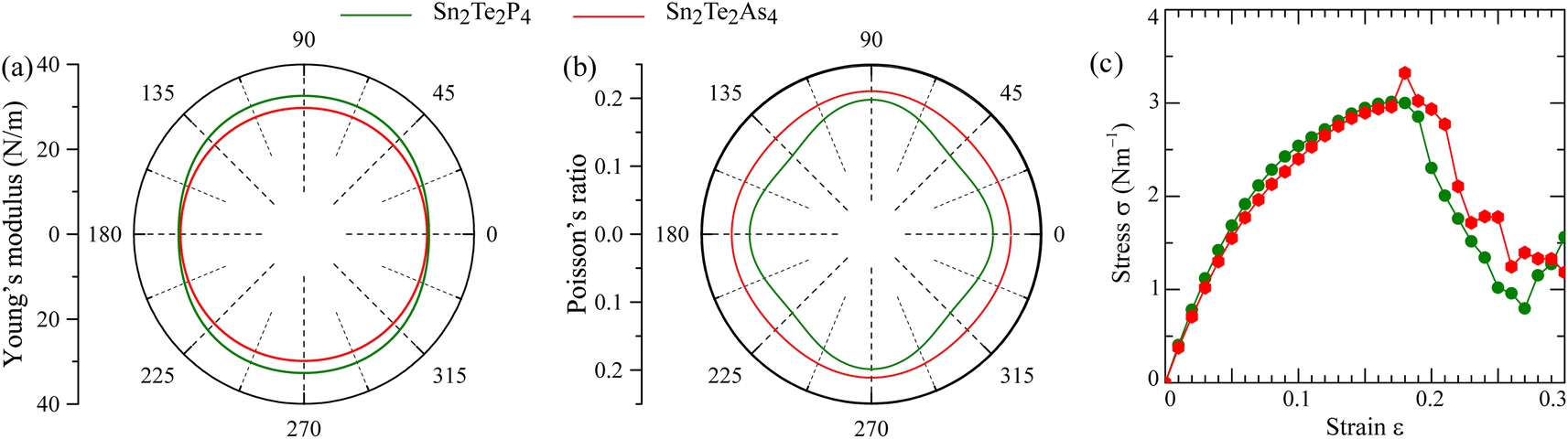 | ||
| Fig. 2 Mechanical properties of Sn2Te2P4 (green lines) and Sn2Te2P4 (red lines) monolayers including (a) Young's modulus and (b) Poisson's ratio as angular functions and (c) dependence of stress (σ) on strain (ε). | ||
3.2 Electronic and optical properties of Sn2Te2X4 (X = P, As) monolayers under strain
It is well-known that members of the AXIV2 BXVI2 CXV4 family (AXIV2 = Sn or Ge, BXVI2 = S or Se and CXV4 = P or As) have appropriate properties for solar energy harvesting.29–31 To study such properties of Sn2Te2P4 and Sn2Te2As4 monolayers, their electronic features are calculated. For the buckling honeycomb configuration, the line connecting Γ–M–K–Γ points is the most symmetric path, along which the band structures can be calculated. The band structures are illustrated in Fig. 3(a) for the Sn2Te2P4 monolayer and in Fig. 3(b) for the Sn2Te2As4 monolayer, where dashed blue curves were obtained by applying the GGA-PBE method and solid red curves were obtained with the HSE06 method. Both methods reveal that Sn2Te2P4 and Sn2Te2As4 monolayers are semiconductors with direct band gaps because their valence band maximum (VBM) and conduction band minimum (CBM) are located at the same Γ-point. The highest valence bands are rather curved at Γ- and K points, indicating good mobility of holes along the Γ–K path in the two monolayers. Meanwhile, the lowest conduction bands are curved only in the vicinity of the Γ point. Therefore, the mobility of electrons is significant near the Γ point. | ||
| Fig. 3 Electronic characteristics of the (a)–(c) Sn2Te2P4 monolayer and (d)–(f) Sn2Te2As4 monolayers: band structure calculated by PBE (blue dashed lines) and HSE06 (red solid lines) methods; partial density of states PDOS and charge density iso-surfaces of the VBM and CBM with an iso-surface value of 0.02 e Å−6; both were calculated by the HSE06 method. | ||
Despite the similarity in the pattern of the GGA-PBE and HSE06 band structures, their band gaps exhibit notable differences (Fig. 3). Because the GGA-PBE method does not include good exchange–correlation of electrons, there is an unphysical component related to the interaction of one electron with itself. This provides extra energy to electrons making them occupy higher energy levels in the valence bands. Meanwhile, the unoccupied states of the conduction bands are not affected. Therefore, the gap between the VBM and CBM becomes smaller than its actual value. The HSE06 method includes some correction to the exchange–correlation interaction. Therefore, the band gap obtained by HSE06 is not reduced. As listed in Table 1, the HSE06 band gap of Sn2Te2P4 is 1.66 eV, which is 0.48 eV larger than the GGA-PBE band gap. For the Sn2Te2As4 monolayer, the difference is also 0.48 eV. The Te atom does excellent work in enlarging the band gap of the pristine monolayers. The band gap of the SnP3 monolayer increases from 0.66 eV (ref. 33) to 1.66 eV as the Te atom is substituted for the P atom to form the Sn2Te2P4 monolayer. Similarly, the monolayer SnAs3 has metallic nature3 because its band gap equals to zero. However, the Te substitution results in the Sn2Te2As4 monolayer, which is a semiconducter with a significant band gap of 1.52 eV.
To study the impact of Te atoms on the expansion of the band gaps in SnP3 and AsP3 monolayers, we calculated and illustrated the density of states (DOS) for Sn2Te2P4 and Sn2Te2As4 monolayers in Fig. 3(b) and (e), respectively. The sp-hybridization of orbitals from Sn and P in the Sn2Te2P4 monolayer or Sn and As in the Sn2Te2As4 monolayer donates a major part to the valence band maxima (VBMs). Meanwhile, the conduction band minima (CBMs) are mainly occupied by s- and p-orbitals from Sn and P (in the case of the Sn2Te2P4 monolayer) and from Sn and As (in the case of the Sn2Te2As4 monolayer). Te atoms are important in both monolayers as their orbitals contribute an important portion to both the VBMs and CBMs. Consequently, the combination of sp-hybridized orbitals from Te and P atoms or from Te and As atoms might result in an increase in energy levels in the conduction bands, which leads to the widening of the band gaps in Sn2Te2P4 and Sn2Te2As4 monolayers. Generally, there is a similar pattern of PDOS in both monolayers, where the VBMs are characterized with high intensity originating from the well hybridized orbitals from all atoms. Meanwhile, the intensity of the CBMs is rather low despite the sp-hybridization observed in these states. To gain better insight into these characteristics, the charge density iso-surfaces of VBMs and CBMs were calculated and are present in Fig. 3(c) for the Sn2Te2P4 monolayer and Fig. 3(f) for the Sn2Te2As4 monolayer. The high orbital hybridization in the valence bands leads to significant VBM density in the regions along atomic bonds. Meanwhile, the CBMs mainly concentrate on the P–P bonds in the Sn2Te2P4 monolayer or As–As bonds in the Sn2Te2As4 monolayer. Some smaller portion of CBM density is also found at the Te sites. It is well-known that CBMs are occupied by photoexcited electrons, while holes occupy the VBMs. Therefore, the Sn2Te2As4 and Sn2Te2As4 monolayers with VBMs and CBMs concentrated in different regions in space are promising materials because their electronic characteristics enhance the electron–hole separation.
It is mentioned above that Sn2Te2P4 and Sn2Te2As4 monolayers have good potential to be applied in flexible devices. It is important to study the variation of their electronic characteristics under certain strains. The two monolayers can bear strain up to about 17%, as depicted in Fig. 2(c). Therefore, the dependence of the band structures and band gaps on the strain ranging from −8% to 8% were calculated and are presented in Fig. 4. It can be seen in Fig. 4(a) that Sn2Te2P4 is a semiconductor with a direct band gap at equilibrium and its band gap retains its direct nature under compressive strain up to −8% and tensile strains up to 2%. When this material experiences a tensile strain of more than 2%, the band gap transitions from being direct to becoming indirect; meanwhile the location of the VBM is at the K point and the CBM is situated on the path connecting K and the Γ point, as illustrated in Fig. 4(c). Despite the fluctuation of the VBM and CBM, as shown in Fig. 4(d), the band gap of the Sn2Te2As4 monolayer retains its direct nature under both compressive and tensile strains. It is worth noting that strain always narrows the band gap of the Sn2Te2P4 monolayer. Meanwhile, the band gap of the Sn2Te2As4 monolayer is decreased by compressive strain and it is widened by tensile strains. Specifically, a tensile strain of 4% causes the largest band gap of the Sn2Te2As4 monolayer.
 | ||
| Fig. 4 Variation in the band gap and band structure of (a and c) Sn2Te2P4 and (b and d) Sn2Te2As4 monolayers subjected to strains ranging from −8% to 8%. | ||
The change in the electronic structure can greatly affect the optical properties of a material. Specifically, the change in the band gap demonstrated above will affect the light absorption rate α(ω) of Sn2Te2P4 and Sn2Te2As4 monolayers. The optical properties of 2D materials can be obtained using Kramers–Kronig equations,56 and the “Joint density of state” theory.57 The absorption rates α(ω) of Sn2Te2P4 and Sn2Te2As4 monolayers under strain from −8% to 8% were calculated and are presented in Fig. 5. Generally, the two monolayers have a rather high absorption rate of a minor part of infrared waves (104 cm−1), visible light (104–105 cm−1) and ultra-violet waves (15–20 × 105 cm−1). This is an advantage for solar energy materials as infrared and visible light carries a major proportion of energy in the solar spectrum reaching Earth. Because the strain basically reduces the band gap of Sn2Te2P4, it causes a slight increase in the α(ω) for infrared and visible light. However, phonons of ultra-violet light carry very high energy which can stimulate the electrons to transfer not only between the VBM and CBM but also from lower valence bands to higher conduction bands. Therefore, the compressive strain (pink and yellow curves), which causes orbital splitting, can increase the absorption rate of ultra-violet light. For the Sn2Te2As4 monolayer, a tensile strain of 4–8% is favorable for absorption of phonons from 1.5–2.5 eV. All strains have a negligible effect on the absorption of phonons from 2.5 to 3.0 eV. For ultra-violet light, the compressive strain also increases the absorption rate α(ω) while the tensile strain decreases this quantity.
 | ||
| Fig. 5 Effect of strains ranging from −8% to 8% on the light absorption rate α(ω) of (a) Sn2Te2P4 and (b) Sn2Te2As4 monolayers. | ||
3.3 Characteristics of Sn2Te2X4 (X = P, As) monolayers as promising photocatalysts
Given the remarkable capacity to absorb solar radiation, Sn2Te2P4 and Sn2Te2As4 monolayers must be investigated for their ability to transform solar energy into other kinds of energy. The work function, usually denoted as Φ, is the least energy required to transfer an electron from the surface to vacuum. For a photocatalyst in water splitting, the work function plays an important role because the free electrons can participate in the redox reactions.58,59 The electrostatic potentials of Sn2Te2P4 and Sn2Te2As4 were calculated and are plotted in Fig. 6 as functions of the distance from the Fermi level. The work function of Sn2Te2P4 and Sn2Te2As4 were determined to be 4.80 eV and 4.95 eV, which are suitable for the photocatalytic water splitting process. It is an advantage of the two monolayers because most photocatalysts with such a work function are favorable for water splitting using solar energy.60,61 | ||
| Fig. 6 Work function Φ of (a) Sn2Te2P4 and (b) Sn2Te2As4 monolayers. | ||
To stimulate the redox reaction in the water splitting process, the VBM and CBM of a semiconductor must be located at suitable positions which are denoted as EVB and ECB, respectively. The energy levels of these positions are determined as ECB = χ − EC − 0.5Eg and EVB = ECB + Eg.62 The constant EC is the energy of a free electron measured on the hydrogen scale, which is 4.5 eV. The term Eg is the band gap of the semiconductor. The average electronegativity χ can be calculated based on the electronegativities of Sn, Te, P, and As atoms, which are denoted as χSn, χTe, χP, and χAs, respectively. There are 8 constituent atoms in the Sn2Te2P4 monolayer or Sn2Te2As4 monolayer including 2 Sn atoms, 2 Te atoms, and 4 P or As atoms. Therefore, the geometric average of these electronegativities is defined as  .63 The incident phonon transfers its energy to an electron making it jump to states in the conduction region which creates hole in the valence bands. Therefore, it is necessary that the CBM is still located at higher energy levels than the reduction potential of H+/H2, so that the excited electron can move to H+ to form hydrogen gas. Meanwhile, the VBM must be located at energy levels lower than the oxidation potential of O2/H2O so that the electron from OH− can move to the VBM, where it fills the hole. This reaction turns anion OH− into water and oxygen gas. As shown in Fig. 7, the VBM and CBM of equilibrium Sn2Te2P4 and Sn2Te2As4 monolayers are suitable for producing hydrogen and oxygen gases. Under strain ranging from −4% to 8%, the water splitting catalytic activity of the Sn2Te2P4 monolayer remains possible. For the Sn2Te2As4 monolayer, all compressive strains and tensile strains higher than 8% inhibit its catalytic activity. A tensile strain of 2–6% can even enhance the photocatalytic water splitting of the Sn2Te2As4 monolayer.
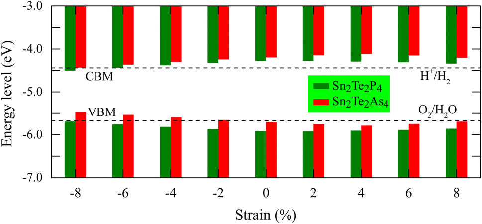 | ||
| Fig. 7 The VBM and CBM positions of Sn2Te2P4 (green) and Sn2Te2As4 (red) in relation to water redox potentials at the normal hydrogen electrode (NHE) and vacuum level. The reduction potential of H+/H2 and the oxidation potential of O2/H2O are marked with dashed black lines. | ||
It is obvious that electrons and holes play an important role in the water splitting process. Therefore, it is necessary to investigate their characteristics. To calculate the charge carrier mobility of a 2D material it is necessary to determine how the energetic characteristics of the system change under uniaxial strains. The uniaxial strain is denoted as εuni and the total energy of the system is Etot. Under strains the CBM and VBM occupy different energy levels. These energy levels are regarded as the band edge alignment and denoted as Eedge. The dependences of C2D on the uniaxial strains εuni ranging from −1% to 1% are presented in Fig. 8(a) and (b) for Sn2Te2P4 and Sn2Te2As4 monolayers, respectively. Fig. 8(c, d) also show the dependences of Ed on εuni in the case of Sn2Te2P4 and Sn2Te2As4 monolayers, respectively. The energy changes due to uniaxial strains εuni along the x-direction are plotted with blue/green colors and the changes due to uniaxial strains εuni along the y-direction are plotted with red/aqua colors. Because the elastic module C2D = ∂2Etot/A∂εuni2) (A is the area of the unit cell) and the deformation energy Ed = ΔEedge/ε are defined as the derivatives Etot and Eedge, respectively, it is necessary to fit the data in Fig. 8 to a polynomial to achieve continuous functions Etot(εuni) and Eedge(εuni). The effective mass m* is also an important parameter and it is determined as 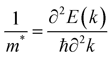 , where E(k) is the energy function of the k-point derived from the DFT calculations and ℏ is the Planck constant. Because the effective masses are calculated along x- and y-directions, the average values
  are defined as
  . The charge carrier mobility for 2D materials μ2D is calculated as
  .64 The coefficients e and kB are the elementary charge and Boltzmann constant, respectively. It can be seen from Table 3 that the charge carrier mobility in the two monolayers strongly depends on the directions. In the Sn2Te2P4 monolayer, the mobility of electrons along the x-direction is 1087.21 cm2 V−1 s−1, which is much higher than 160.01 cm2 V−1 s−1 of electrons along the y-direction. Moreover, it is also higher than the mobility of holes in both x- and y-directions. This is an advantage of Sn2Te2P4 as a photocatalyst because it promotes electron–hole separation. In the case of the Sn2Te2As4 monolayer, the mobility of electrons and holes along the x-direction is nearly of the same magnitude, which is 763.76 cm2 V−1 s−1 and 654.77 cm2 V−1 s−1, respectively. These values are nearly reduced by half along the y-direction. It is worth noting that the charge carrier mobilities in Sn2Te2P4 and Sn2Te2As4 monolayers are higher than those in SnP3 and GeP3 monolayers.17,22
 | ||
| Fig. 8 Total energy Etot(εuni) (a) and band edge alignment ΔEedge (b) as functions of uniaxial strains εuni along x- and y-directions. | ||
|
|
|
C 2D x | C 2D y | E d x | E d y | μ x | μ y | ||
|---|---|---|---|---|---|---|---|---|---|
| a Ref. 22. b Ref. 17. | |||||||||
| Electron | Sn2Te2P4 | 1.39 | 0.17 | 25.98 | 24.14 | 0.87 | −6.35 | 1087.21 | 160.01 |
| Sn2Te2As4 | 1.27 | 0.14 | 22.04 | 21.82 | 1.06 | −5.68 | 763.76 | 231.59 | |
| SnP3 | 0.90a | 0.90a | 270.00a | 190.00a | |||||
| GeP3 | 0.59b | 0.80b | 70.00b | 40.00b | |||||
| Hole | Sn2Te2P4 | 0.65 | 0.12 | 25.98 | 24.14 | −2.79 | −5.96 | 391.27 | 421.93 |
| Sn2Te2As4 | 0.59 | 0.10 | 22.04 | 21.82 | −2.25 | −7.05 | 654.77 | 407.48 | |
| SnP3 | 0.72a | 1.64a | 360.00a | 170.00a | |||||
| GeP3 | 1.00b | 2.75b | 190.00b | 14.00b | |||||


The solar to hydrogen efficiency (ηSTH) is an important parameter to estimate the efficiency of the Sn2Te2P4 and Sn2Te2As4 monolayers in the conversion of solar energy into hydrogen energy. It can be calculated using light absorption efficiency ηabs, carrier utilization ηcu, the difference in the CBM potential and reduction potential of H+/H2χ(H2) and the difference in the VBM potential and oxidation potential of O2/H2O χ(O2). The details of the calculation are presented in the ESI† and the calculated values are listed in Table 4. Because of the small band gaps, both Sn2Te2P4 and Sn2Te2As4 monolayers have a great ability to convert light into energy, with a light absorption efficiency of above 50%, as shown in Table 4. As mentioned in the above sections, the two monolayers have a high absorption rate of a wide range of solar waves. This enhances the amount of photo-generated electrons and holes. Besides, the mobility of charge carriers strongly depends on the direction and the type of charge carriers leading to better electron–hole separation. These two advantages contribute to the high carrier utilization of the two monolayers. The high ηabs and ηcu lead to high ηSTH of Sn2Te2P4 and Sn2Te2As4 monolayers, which is 17.12% and 15.76%, respectively. These values are close to the limit of 18% predicted by theoretical calculation65 and they are higher than that of some famous photocatalysts such as WSSe and PdSe2.66,67
| χ(H2) (eV) | χ(O2) | η abs | η cu | η STH | |
|---|---|---|---|---|---|
| Sn2Te2P4 | 0.170 | 0.256 | 53.42 | 32.05 | 17.12 |
| Sn2Te2As4 | 0.253 | 0.042 | 60.31 | 26.13 | 15.76 |
4 Conclusion
This study introduces two new monolayers Sn2Te2P4 and Sn2Te2As4 to the AXIV2 BXVI2 CXV4 family, where AXIV, BXVI and CXV represent elements from groups XIV, XVI, and XV, respectively. The first-principles calculation was performed to study the structural and electronic properties of the two monolayers. The stability of the new monolayers was confirmed by energetic, dynamic and mechanical evaluation. The two monolayers have a rather low Young's modulus but their Poisson's ratio is close to that of graphene. The materials are ductile and tough and are promising for flexible devices. The two monolayers Sn2Te2P4 and Sn2Te2As4 can withstand a strain up to 17%. Sn2Te2P4 and Sn2Te2As4 monolayers are semiconductors with a direct band gap, the magnitude of which is greatly affected by the sp-hybridization of orbitals from Te atoms. Besides, the strain can vary the magnitudes of the band gap but the nature of Sn2Te2P4's band gap changes from direct into indirect only under tensile strain higher than 2%. Strain can slightly affect the magnitude of the light absorption rate in the infrared and visible regions. However, compressive strain can significantly improve the absorption of ultra-violet light. Both Sn2Te2P4 and Sn2Te2As4 are promising photocatalysts due to their high absorption rate (104–105 cm−1) over a wide range of the solar spectrum. Their charge carrier mobility is rather high and it is favorable for electron–hole separation. Their work functions are 4.80–4.95 eV, which is suitable for the water splitting process. Besides, the VBM and CBM of the two monolayers are located at suitable positions to stimulate the redox reaction. Finally, the two monolayers possess high solar to hydrogen efficiency with ηSTH in the range of 15.76–17.12%.Conflicts of interest
There are no conflicts of interest to declare.Data availability
The data that support the findings of this study are available upon reasonable request from the corresponding author.References
- C. Zhang, K. Ren, S. Wang, Y. Luo, W. Tang and M. Sun, J. Phys. D: Appl. Phys., 2023, 56, 483001 CrossRef CAS.
- A. Elbanna, H. Jiang, Q. Fu, J.-F. Zhu, Y. Liu, M. Zhao, D. Liu, S. Lai, X. W. Chua and J. Pan, et al. , ACS Nano, 2023, 17, 4134–4179 CrossRef CAS PubMed.
- N. H. Solangi, R. R. Karri, N. M. Mubarak, S. A. Mazari and A. K. Azad, J. Energy Storage, 2023, 70, 108004 CrossRef.
- S. Aftab, M. Z. Iqbal and M. W. Iqbal, Adv. Mater. Interfaces, 2022, 9, 2201219 CrossRef CAS.
- K. Thakar and S. Lodha, in 2D Materials for Electronics, Sensors and Devices, Elsevier, 2023, pp. 207–258 Search PubMed.
- X. Tan, S. Wang, Q. Zhang, J. He, S. Chen, Y. Qu, Z. Liu, Y. Tang, X. Liu and C. Wang, et al. , Nanoscale, 2023, 15, 9297–9303 RSC.
- T. V. Vu, V. H. Chu, J. Guerrero-Sanchez and D. Hoat, ACS Appl. Electron. Mater., 2024, 6, 3647–3656 CrossRef CAS.
- T. Dutta, N. Yadav, Y. Wu, G. J. Cheng, X. Liang, S. Ramakrishna, A. Sbai, R. Gupta, A. Mondal and Z. Hongyu, et al. , Nano Mater. Sci., 2024, 6, 1–23 CrossRef CAS.
- T. V. Vu, V. T. Vi, N. T. Hiep, K. V. Hoang, A. Kartamyshev, H. V. Phuc and N. N. Hieu, RSC Adv., 2024, 14, 21982–21990 RSC.
- T. V. Vu, K. M. Bui, K. V. Hoang, A. I. Kartamyshev, H. H. Thi, A. A. Lavrentyev, N. P. Q. Anh, H. V. Phuc and N. N. Hieu, J. Phys. D: Appl. Phys., 2024, 57, 345304 CrossRef.
- Y. Luo, Y. He, Y. Ding, L. Zuo, C. Zhong, Y. Ma and M. Sun, Inorg. Chem., 2023, 63, 1136–1141 CrossRef.
- Y. Yin, Y. Zhou, M. H. Rafailovich and C.-Y. Nam, Nanotechnology, 2023, 34, 172001 CrossRef.
- J. Cho, H. S. Radhakrishnan, R. Sharma, M. R. Payo, M. Debucquoy, A. van der Heide, I. Gordon, J. Szlufcik and J. Poortmans, Sol. Energy Mater. Sol. Cells, 2020, 206, 110324 CrossRef CAS.
- P. Tang, J.-H. Yuan, Y.-Q. Song, M. Xu, K.-H. Xue and X.-S. Miao, J. Mater. Sci., 2019, 54, 12676–12687 CrossRef CAS.
- F. Li, H. Wu, Z. Meng, R. Lu and Y. Pu, J. Phys. Chem. Lett., 2019, 10, 761–767 CrossRef CAS.
- N. Lu, Z. Zhuo, H. Guo, P. Wu, W. Fa, X. Wu and X. C. Zeng, J. Phys. Chem. Lett., 2018, 9, 1728–1733 CrossRef CAS.
- Y. Jing, Y. Ma, Y. Li and T. Heine, Nano Lett., 2017, 17, 1833–1838 CrossRef CAS.
- A. Jalil, Z. Zhuo, Z. Sun, F. Wu, C. Wang and X. Wu, J. Mater. Chem. A, 2020, 8, 1307–1314 RSC.
- N. Miao, B. Xu, N. C. Bristowe, J. Zhou and Z. Sun, J. Am. Chem. Soc., 2017, 139, 11125–11131 CrossRef CAS PubMed.
- M. Laurien, H. Saini and O. Rubel, Phys. Chem. Chem. Phys., 2021, 23, 7418–7425 RSC.
- M. Xie, Y. Li, X. Liu, J. Yang, H. Li and X. Li, Phys. Chem. Chem. Phys., 2022, 24, 20694–20700 RSC.
- S. Sun, F. Meng, H. Wang, H. Wang and Y. Ni, J. Mater. Chem. A, 2018, 6, 11890–11897 RSC.
- S. Yao, X. Zhang, Z. Zhang, A. Chen and Z. Zhou, Int. J. Hydrogen Energy, 2019, 44, 5948–5954 CrossRef CAS.
- Y. Zhang, X. Jia, S. Liu, B. Zhang, K. Lin, J. Zhang and G. Conibeer, Sol. Energy Mater. Sol. Cells, 2021, 225, 111073 CrossRef CAS.
- S. Bremner, C. Yi, I. Almansouri, A. Ho-Baillie and M. Green, Sol. Energy, 2016, 135, 750–757 CrossRef CAS.
- A. N. Andriotis, E. Richter and M. Menon, Phys. Rev. B, 2016, 93, 081413 CrossRef.
- Q. Xie, J. Yuan, N. Yu, L. Wang and J. Wang, Comput. Mater. Sci., 2017, 135, 160–164 CrossRef CAS.
- Y. Ding and Y. Wang, Phys. Chem. Chem. Phys., 2018, 20, 6830–6837 RSC.
- Y.-L. Zhu, J.-H. Yuan, Y.-Q. Song, K.-H. Xue, S. Wang, C. Lian, Z.-N. Li, M. Xu, X.-M. Cheng and X.-S. Miao, Int. J. Hydrogen Energy, 2019, 44, 21536–21545 CrossRef CAS.
- Y.-L. Liu, X.-X. Jiang, B. Li, Y. Shi, D.-S. Liu and C.-L. Yang, Appl. Phys. Lett., 2021, 119, 143102 CrossRef CAS.
- T. V. Vu, N. N. Hieu, D. D. Vo, A. Kartamyshev, H. D. Tong, T. T. Trinh, V. Khuong Dien, Z. Haman, P. Dey and N. Khossossi, J. Phys. Chem. C, 2024, 128, 4245–4257 CrossRef CAS.
- M. S. Ramzan, V. Bacic, Y. Jing and A. Kuc, J. Phys. Chem. C, 2019, 123, 25470–25476 CrossRef CAS.
- A. Slassi, S. M. Gali, A. Pershin, A. Gali, J. Cornil and D. Beljonne, J. Phys. Chem. Lett., 2020, 11, 4503–4510 CrossRef CAS PubMed.
- G. Kresse and J. Furthmüller, Phys. Rev. B: Condens. Matter Mater. Phys., 1996, 54, 11169–11186 CrossRef CAS PubMed.
- G. Kresse and D. Joubert, Phys. Rev. B: Condens. Matter Mater. Phys., 1999, 59, 1758 CrossRef CAS.
- J. P. Perdew, K. Burke and M. Ernzerhof, Phys. Rev. Lett., 1996, 77, 3865 CrossRef CAS PubMed.
- J. Heyd, G. E. Scuseria and M. Ernzerhof, J. Chem. Phys., 2003, 118, 8207–8215 CrossRef CAS.
- L. Bengtsson, Phys. Rev. B: Condens. Matter Mater. Phys., 1999, 59, 12301 CrossRef CAS.
- S. Grimme, J. Antony, S. Ehrlich and H. Krieg, J. Chem. Phys., 2010, 132, 154104 CrossRef.
- V. Wang, N. Xu, J.-C. Liu, G. Tang and W.-T. Geng, Comput. Phys. Commun., 2021, 267, 108033 CrossRef CAS.
- T. Sohier, M. Calandra and F. Mauri, Phys. Rev. B, 2017, 96, 075448 CrossRef.
- L. Chaput, A. Togo, I. Tanaka and G. Hug, Phys. Rev. B: Condens. Matter Mater. Phys., 2011, 84, 094302 CrossRef.
- J. Bardeen and W. Shockley, Phys. Rev., 1950, 80, 72 CrossRef CAS.
- D. A. Aksyonov, S. S. Fedotov, K. J. Stevenson and A. Zhugayevych, Comput. Mater. Sci., 2018, 154, 449–458 CrossRef CAS.
- B. Ghosh, S. Puri, A. Agarwal and S. Bhowmick, J. Phys. Chem. C, 2018, 122, 18185–18191 CrossRef CAS.
- Y. Guo, S. Zhou, Y. Bai and J. Zhao, Appl. Phys. Lett., 2017, 110, 163102 CrossRef.
- F. Mouhat and F.-X. Coudert, Phys. Rev. B: Condens. Matter Mater. Phys., 2014, 90, 224104 CrossRef.
- D. D. Vo, T. V. Vu, A. Lavrentyev, O. Khyzhun, A. Kartamyshev, H. D. Tong and N. N. Hieu, New J. Chem., 2023, 47, 9124–9133 RSC.
- T. V. Vu, H. V. Phuc, L. T. T. Phuong, V. T. T. Vi, A. I. Kartamyshev and N. N. Hieu, Nanoscale Adv., 2024, 6, 4128–4136 RSC.
- C. Lee, X. Wei, J. W. Kysar and J. Hone, Science, 2008, 321, 385–388 CrossRef CAS PubMed.
- B. Mortazavi, O. Rahaman, M. Makaremi, A. Dianat, G. Cuniberti and T. Rabczuk, Phys. E Low-Dimens. Syst. Nanostruct., 2017, 87, 228–232 CrossRef CAS.
- Q. Peng, X. Sun, H. Wang, Y. Yang, X. Wen, C. Huang, S. Liu and S. De, Appl. Mater. Today, 2017, 7, 169–178 CrossRef.
- P. Hess, Phys. Chem. Chem. Phys., 2018, 20, 7604–7611 RSC.
- Y. Jiang, Y. Zhang, Q. Huang, L. Hao and S. Du, J. Mater. Res. Technol., 2020, 9, 14979–14989 CrossRef CAS.
- K. Liu, Q. Yan, M. Chen, W. Fan, Y. Sun, J. Suh, D. Fu, S. Lee, J. Zhou and S. Tongay, et al. , Nano Lett., 2014, 14, 5097–5103 CrossRef CAS PubMed.
- E. A. Moore and L. E. Smart, in Solid State Chem., CRC Press, 2020, pp. 283–314 Search PubMed.
- M. Gajdoš, K. Hummer, G. Kresse, J. Furthmüller and F. Bechstedt, Phys. Rev. B: Condens. Matter Mater. Phys., 2006, 73, 045112 CrossRef.
- A. R. Zeradjanin, A. Vimalanandan, G. Polymeros, A. A. Topalov, K. J. Mayrhofer and M. Rohwerder, Phys. Chem. Chem. Phys., 2017, 19, 17019–17027 RSC.
- J. Y. Cheon, J. H. Kim, J. H. Kim, K. C. Goddeti, J. Y. Park and S. H. Joo, J. Am. Chem. Soc., 2014, 136, 8875–8878 CrossRef CAS.
- Y. Wang, T. Liu, W. Tian, Y. Zhang, P. Shan, Y. Chen, W. Wei, H. Yuan and H. Cui, RSC Adv., 2020, 10, 41127–41136 RSC.
- K. Kočí, L. Matějová, N. Ambrožová, M. Šihor, I. Troppová, L. Čapek, A. Kotarba, P. Kustrowski, A. Hospodková and L. Obalová, J. Sol-Gel Sci. Technol., 2016, 78, 550–558 CrossRef.
- Q. Li, H. Meng, P. Zhou, Y. Zheng, J. Wang, J. Yu and J. Gong, ACS Catal., 2013, 3, 882–889 CrossRef CAS.
- Q. Yuan, L. Chen, M. Xiong, J. He, S.-L. Luo, C.-T. Au and S.-F. Yin, Chem. Eng. J., 2014, 255, 394–402 CrossRef CAS.
- S. Bruzzone and G. Fiori, Appl. Phys. Lett., 2011, 99, 222108 CrossRef.
- C.-F. Fu, J. Sun, Q. Luo, X. Li, W. Hu and J. Yang, Nano Lett., 2018, 18, 6312–6317 CrossRef CAS PubMed.
- L. Ju, M. Bie, X. Tang, J. Shang and L. Kou, ACS Appl. Mater. Interfaces, 2020, 12, 29335–29343 CAS.
- C. Long, Y. Liang, H. Jin, B. Huang and Y. Dai, ACS Appl. Energy Mater., 2018, 2, 513–520 CrossRef.
Footnote |
| † Electronic supplementary information (ESI) available. See DOI: https://doi.org/10.1039/d4na00563e |
| This journal is © The Royal Society of Chemistry 2024 |