
 Open Access Article
 This Open Access Article is licensed under a
 Creative Commons Attribution 3.0 Unported Licence
Unveiling the complex phonon nature and phonon cascades in 1L to 5L WSe2 using multiwavelength excitation Raman scattering†
Claire
Blaga
a,
Ángel
Labordet Álvarez
b,
Akshay
Balgarkashi
 a,
Mitali
Banerjee
c,
Anna
Fontcuberta i Morral
ad and
Mirjana
Dimitrievska
*ab
a,
Mitali
Banerjee
c,
Anna
Fontcuberta i Morral
ad and
Mirjana
Dimitrievska
*ab
aLaboratory of Semiconductor Materials, Institute of Materials, School of Engineering, École Polytechnique Fédérale de Lausanne, 1015 Lausanne, Switzerland
bNanomaterials Spectroscopy and Imaging Group, Transport at Nanoscale Interfaces Laboratory, Swiss Federal Laboratories for Material Science and Technology (EMPA), Ueberlandstrasse 129, 8600 Duebendorf, Switzerland. E-mail: mirjana.dimitrievska@empa.ch
cLaboratory of Quantum Physics, Topology and Correlations, Institute of Physics, School of Basic Sciences, Ecole Polytechnique Fédérale de Lausanne, 1015 Lausanne, Switzerland
dInstitute of Physics, School of Basic Sciences, Ecole Polytechnique Fédérale de Lausanne, 1015 Lausanne, Switzerland
First published on 30th July 2024
Abstract
Tungsten diselenide (WSe2) is a 2D semiconducting material, promising for novel optoelectronic and phononic applications. WSe2 has complex lattice dynamics and phonon structure. Numerous discrepancies in the literature exist regarding the interpretation and identification of phonon modes. This work presents a complete investigation of the vibrational properties of 1L to 5L flakes and bulk WSe2 using multi-wavelength Raman spectroscopy. We especially highlight measurements using 785 nm excitation, which have not been performed before. These allow us to solve inconsistences in the literature in terms of defect-activated non-Γ point single phonon modes and Breit–Wigner–Fano type resonance. We identify 35 Raman peaks per flake thickness, which we attribute to either one-phonon or multi-phonon modes, including two-phonon scattering due to a van Hove singularity (vHs). The measurements are in excellent agreement with the theoretical predictions. Using photoluminescence measurements, we identify photon-exciton coupling leading to resonant Raman scattering, suggesting wavelength laser excitations best suited for further investigations of specific WSe2 flake thicknesses. Finally, we report the observation of phonon-cascades for all WSe2 flake thicknesses, indicating strong phonon–electron interactions during early carrier relaxation processes in WSe2. This research provides a solid foundation and reference for future investigations of the vibrational properties of WSe2, paving the way for further development of this material towards applications.
Introduction
Research on two-dimensional (2D) materials, ignited by the discovery of graphene, has led to the revelation of a multitude of layered materials with promising properties. The family of transition metal dichalcogenides (TMDs) is of particular significance. TMDs are composed of three atom-thick monolayers, made up of a transition metal atom layer sandwiched between two chalcogen atom layers. Unlike graphene, some TMDs, such as MoS2 and WSe2, are semiconductors with bandgaps in the visible range (1–2.5 eV).1–3 They exhibit thickness-dependent properties resulting from symmetry breaking and quantum confinement. WSe2 and MoS2 show an indirect to direct bandgap transition when going from multi- to monolayer thickness, exhibiting bright photoluminescence from strongly bound excitons in the latter case.1 TMDs host valley-selective excitons, opening a door towards valley-based optoelectronic engineering.4 WSe2, in particular, has been shown to host deterministically engineered single photon emission.5 Despite being ideal candidates for many ultra-thin optoelectronic applications, there are still open questions concerning their phononic properties.Understanding the vibrational (phononic) properties of thin layer TMDs is crucial for applications requiring the engineering of thermal conductivity.6–8 It is also essential for leveraging the interlayer charge transfer dynamics in van der Waals heterostructures,9,10 particularly for optoelectronic and photovoltaic applications, and the investigation of Moiré phonons in twisted layers of TMDs for novel phononic devices.11
Raman spectroscopy is a routinely used technique for the characterization of 2D materials, as it provides information on the structure,12,13 defect type and density,14,15 and strain of the lattice.16–18 It also gives access to a variety of electronic parameters such as the charge carrier density,19,20 maximum charge carrier mobility,17,21 phonon–electron coupling and electron–electron scattering.22,23 Considering the plethora of information that Raman spectroscopy can provide, a precise comprehension of the Raman spectra and the lattice dynamics is crucial for their further development and utilization in future applications.
Vibrational properties of few-layered WSe2 have been explored in several studies before, where most of the effort was made on the proper interpretation of Raman peaks of WSe2.24–32 Many of these studies show significant discrepancies in the analysis of the Raman spectra and assignment of phonon modes. For example, the interpretation of Raman peaks and assigned phonon modes vary across the literature, from 17 to 42 phonon modes observed.24–32 Interestingly, several studies report activation of non-Γ point single phonon modes in the Raman spectra of WSe2 flakes.30,33,34 These modes are usually not expected in the Raman spectrum of high crystal quality materials, as they require the presence of defects in order to be activated.35–37 Some studies report the observation of the Breit–Wigner–Fano (BWF) type resonance of the low intensity Raman peak at 302 cm−1 assigned to WSe2.30 This is very unusual, as theoretically calculated phonon frequencies do not predict the presence of any single or multi-phonon mode at this position. Finally, one finds different interpretations of the Raman peak at 260 cm−1, from the identification as a broad 2LA(M) mode, to the deconvolution into a dozen peaks assigned to one-phonon and multi-phonon modes.33,34,38 Such inconsistencies in reported results require clarification by a systematic review of published data and an in-depth investigation of vibrational properties of multilayer WSe2 systems.
In this work, we investigate vibrational properties of multilayer (1L to 5L) and bulk WSe2 using multiwavelength excitation Raman spectroscopy. Using a rigorous deconvolution process of the Raman spectra measured with 488, 532 and 785 nm laser excitations, we provide a complete analysis of all Raman active modes of WSe2 systems. To the best of our knowledge, this is the first comprehensive analysis of the Raman spectra of WSe2 measured at 785 nm, along with a concise comparison of theoretical and experimental results in terms of phonon symmetries and frequencies. We also shed new light on the inconsistencies reported in the literature regarding the activation of non-Γ point single phonon modes and BWF type resonance. Finally, we highlight the observation of the phonon cascades in 1L to 5L and bulk WSe2 as well as suggest the optimal laser excitations under which different numbers of layers could be further explored. These results can be used as a reference for future studies of vibrational properties of WSe2, paving the way for successful integration of WSe2 in phononic and optoelectronic devices.
Materials and methods
Material preparation
The multi-layered WSe2 flake was obtained by mechanical exfoliation by thinning down a crystal of bulk WSe2 (HQ graphene) with Scotch tape. The thinned crystals were transferred onto a silicon chip covered with 285 nm of SiO2 (NOVA Electronic Materials) using Scotch tape.Characterization
Raman and photoluminescence (PL) measurements were performed on a WITec Alpha 300 R confocal Raman microscope in backscattering geometry. Multiwavelength excitation Raman measurements were performed using 488, 532, and 785 nm lasers. The beam was focused on the sample with a microscope objective, resulting in a diameter spot of 800 nm for the 488 nm laser, 1 μm for the 532 nm laser, and 1.2 μm for the 785 nm laser, and reaching a radiant output power of the order of 500 μW, equivalent to 150 μW at the sample. Laser power conditions were selected based on a power study that measured the Raman spectrum at the same point on the material with increasing laser power densities, starting from the lowest power available. For each laser power, the spectrum was monitored for changes in peak positions, peak widths, or the appearance of new peaks. The highest power for which no changes in these parameters were observed was taken as the optimal laser power for measurements. The backscattered light was analyzed with two spectrometers: a 300 mm lens-based spectrometer with a grating of 1800 g mm−1 equipped with a thermoelectrically cooled CCD for 488 and 532 nm excitation and a 400 mm lens-based spectrometer with a grating of 1200 g mm−1 equipped with a cooled deep-depletion CCD for 785 nm excitation. All Raman peak positions were calibrated with respect to the Si Raman peak at 520 cm−1.Atomic force microscopy (AFM) measurements were performed on a Bruker FastScan AFM, using a ScanAsyst_Fluid+ tip. The AFM mapping is performed in tapping-mode to ensure that the flake does not incur any damage from contact with the tip.
The optical microscopy images were taken with a BX53M Olympus microscope, using a 6.4 megapixel DP23 Olympus digital color camera and an LMPLFLN100x objective.
Results and discussion
Morphological assessment of the WSe2 flake
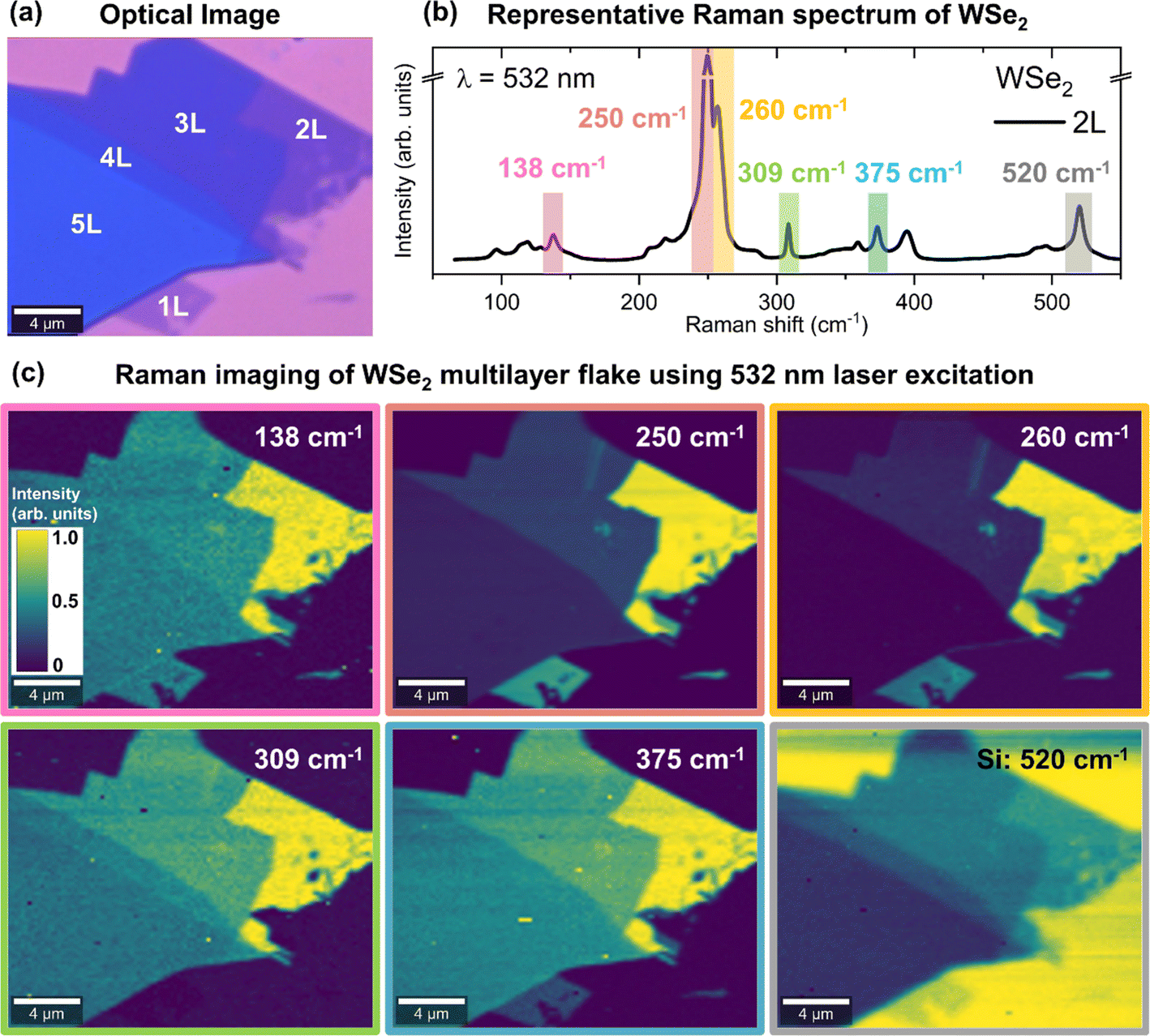
The morphological characterization of the WSe2 flake, as well as the determination of the number of layers, was performed using optical microscopy, AFM and Raman imaging. Fig. 1a shows the optical microscopy image of the flake prior to any further characterization. The optical contrast can be used to empirically determine the thickness of the different parts of the flake. The thickness of the flake is directly correlated with its transparency, with thinner areas being more transparent. The exact number of layers is determined from AFM measurements, which reliably allows to discriminate between different thicknesses as shown in Fig. 1b. This allowed determination of the regions of monolayer (1L), bilayer (2L), three-layer (3L), four-layer (4L) and five-layer (5L) as labeled in Fig. 1. The height profiles of the different layers confirming this assignment are shown in Fig. S1 in the ESI.† | ||
| Fig. 1 Morphological characterization of a WSe2 flake on a SiO2/Si substrate. (a) Optical microscopy image showing different contrasts within the WSe2 flake attributed to different numbers of layers: monolayer (1L), bilayer (2L), three-layer (3L), four-layer (4L) and five-layer (5L). (b) AFM image of the WSe2 flake measured in tapping-mode showing the height profile and confirming the assignment of the different numbers of layers. | ||
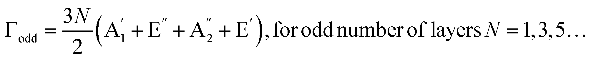
In order to confirm the homogeneity and high crystal quality of the WSe2 flake, we have performed high-resolution Raman imaging using 532 nm laser excitation with a laser spot diameter of 1 μm, as shown in Fig. 2. It should be noted that before any Raman measurements, a laser power study was performed on the small area of the monolayer, which was used to determine the maximal laser power. A consequence of the power study is structural damage to the small area of the monolayer, which is noticeable by the dark spot in Fig. 2a. This area was excluded from any further analysis that was performed in this study.
 | ||
| Fig. 2 Raman imaging of the multilayer WSe2 flake. (a) Optical image of the flake using a Raman microscope. (b) Representative spectrum of the WSe2 flake recorded on the bilayer area using an excitation wavelength of 532 nm. The main peaks are highlighted on the spectrum and their respective intensities over the flake are shown in the Raman images in (c). | ||
Fig. 2b shows a representative Raman spectrum of bilayer (2L) WSe2, highlighting some of the most intense Raman peaks at 138, 250, 260, 309 and 375 cm−1 of WSe2, as well as the 520 cm−1 peak corresponding to the Si substrate. Variations in the Raman intensity of these peaks over the WSe2 flake are shown in the Raman mapping images in Fig. 2c. It can be observed that there is no notable change in the intensity of Raman peaks within each area of a single thickness, for all presented Raman maps. This signals structural uniformity of layers. Additionally, we can observe that the Raman intensity variation between different layers changes depending on which Raman peak is used for imaging. For example, Raman maps corresponding to the intensity of 250 and 260 cm−1 peaks show clear differences in the 1L and 2L areas. The difference between 3L, 4L and 5L is harder to distinguish. On the other hand, the Raman intensity maps corresponding to 309 and 375 cm−1 peaks show the difference among 2L, 3L, 4L and 5L better, while making the identification of 1L areas difficult. Indeed, in the case of 1L, the 375 cm−1 peak has very low intensity and the 309 cm−1 peak is not active. In contrast, Raman imagining with low frequency peaks, such as 138 cm−1, does not show any major differences in the areas corresponding to different numbers of layers. Interestingly, the best imaging of the differences in the number of layers is achieved with Raman mapping of the Si peak at 520 cm−1, enabling clear differentiation between 1L and 5L areas. We attribute this to the absorbance of the Si Raman emission by the layers, similarly to the work of Negri et al.39 This illustrates the potential of using Raman imaging as a complementary method for the identification of the number of layers, when AFM measurements are not possible. However, care should be taken when selecting the Raman peaks used for imaging, depending on the number of layers that need to be identified.
Phonon modes and phonon dispersion in multilayer WSe2
Bulk 2H-WSe2 belongs to the space group D46h (P63/mmc) with the unit cell containing two W and four Se atoms. Group theory analysis predicts the following set of irreducible representations at the Γ point of the Brillouin zone:40–42| Γtotal = A1g + 2A2u + 2B2g + B1u + E1g + 2E1u + 2E2g + E2u. |
Raman and infra-red active modes are:
| ΓRaman = A1g + E1g + 2E2g |
| ΓIR = 2A2u + 2E1u |
In contrast to the bulk, multilayer WSe2 systems are considered quasi 2D, due to the lack of translation symmetry along the c-axis direction. Their space group symmetry is determined by the parity of the number of layers. An odd number of layers is classified within the D3h point group symmetry (without inversion symmetry), while an even number of layers belongs to the D3d point group symmetry (with a center of inversion). The labeling of phonon modes is different depending on the number of layers, and the irreducible representations at the Γ point of the Brillouin zone are:40–42

Therefore, strictly speaking, the notations of the modes for the multilayer WSe2 systems differ, with A1g and E2g modes for bulk, translating to  and E′ modes for an odd number of layers and A1g and Eg modes for an even number of layers.
The one-phonon modes described above, arising from the Γ point, are a result of the first-order Raman scattering process. Higher-order Raman scattering processes are also possible. These involve the combination of multiple phonon modes from Γ and non-Γ points of the Brillouin zone for which the conservation of the momentum rule is preserved. This means combining two (or more) phonons from the Γ point which have zero momentum, or combining phonons from M and K points (or anywhere else in the Brillouin zone) whose total momentum is zero (for example pairs of phonons with equal and opposite momentum). Higher-order Raman scattering is less probable than the first-order, and therefore the combination modes in the Raman spectrum have lower intensities and higher widths of peaks when compared to the first-order Raman modes. These intensities can be significantly enhanced under Raman resonant conditions, when the excitation wavelength is close to the energy of some interband transition in the material. Therefore, for a complete interpretation of the Raman spectrum, it is important to consider the full phonon and energy band dispersion of the material, over the whole Brillouin zone.
The band structure and phonon dispersions of bulk and multilayer WSe2 systems have been extensively studied and reported in the literature.25,27–29,33,34,43–45 For convenience, Fig. S2 in the ESI† presents the density functional theory (DFT) calculated phonon dispersions of monolayer (1L) WSe2 adapted from ref. 33. Monolayer WSe2 has three atoms per unit cell, resulting in a total of nine phonons. The three acoustic phonons correspond to the out-of-plane (ZA) vibrations, in-plane transverse (TA) vibrations, and in-plane longitudinal (LA) vibrations. These phonons are located at 0 cm−1 at the Γ point and correspond to the lowest frequency phonon branches across the Brillouin zone in Fig. S2.† The E′′ and E′ phonon modes are located at 176 and 250 cm−1 at the Γ point, and as doubly degenerated modes, they are split into two optical branches each, over the Brillouin zone. The lower frequency phonon branches correspond to transverse (TO1 and TO2) vibrations, while the higher frequency phonon branches correspond to longitudinal (LO1 and LO2) vibrations of E′′ and E′ modes, respectively. The 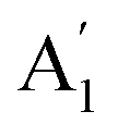 and
and  modes are located at 250 and 310 cm−1 at the Γ point and correspond to two out of plane (ZO1 and ZO2) vibrations, respectively. They are represented by the highest frequency phonon branches in Fig. S2.†
In comparison, the phonon dispersions of the multilayer WSe2 systems (2L, 3L and higher) slightly differ from those of the monolayer WSe2. The main difference is in the number of expected phonons, i.e. phonon branches, with the total number of phonons being calculated as 3N, where N is the number of atoms per unit cell. Therefore, bilayer (2L) WSe2, having 6 atoms per unit cell, will have a total of 18 phonon branches, while trilayer (3L) WSe2, with 9 atoms per unit cell, will have a total of 27 phonon branches, etc. The new phonon branches in the multilayer systems arise from the splitting of the monolayer phonon branches. Therefore, the frequencies of these new phonons are very close to the one of the original monolayer phonon branch. This is the main reason why the overall phonon dispersion of WSe2 looks very similar regardless of the number of layers.33 Another difference is the appearance of the low frequency shear and breathing modes, which arise due to the interlayer van der Waals (vdW) coupling between the layers. Their frequencies depend on the number of layers present.43
It should be noted that the DFT predicted frequencies of the phonon modes, especially at Γ, M and K points of the Brillouin zone, are very important and will be used for the identification of the combination phonon modes in the Raman spectra of WSe2 multilayer systems.
Raman spectra and phonon mode identification in multilayer and bulk WSe2
Fig. 3 shows the Raman spectra of 1L–5L and bulk WSe2 measured at 488, 532 and 785 nm excitation wavelengths. The measurements were performed at room temperature under the same acquisition conditions for all layers, including density of laser power and acquisition times. This allows for comparison of the absolute Raman intensities among the different layers and enables identification of conditions leading to a significant increase in intensity, for example close to Raman resonant conditions. Fig. 3a–c show the comparison of Raman spectra at the absolute intensity scale, while Fig. 3d–e present a magnified intensity scale, allowing better observation of all Raman active peaks. Large differences in the shape of the Raman spectra with changes in the laser wavelength are observed. The highest intensity of Raman peaks is seen for 5L, 2L and bulk when measured with 488, 532 and 785 nm wavelength excitations, respectively. Additionally, we observe that spectral fingerprints, in the frequency regions from 50 to 200 cm−1, look similar for 488 and 532 nm laser excitations, while a significant difference is seen in the case of 785 nm excitation. A similar conclusion can be made for the frequency region from 300 to 500 cm−1. On the other hand, the spectral features do not change significantly with the change in the number of layers. The main difference in this case is observed in the change in the intensity of the peaks.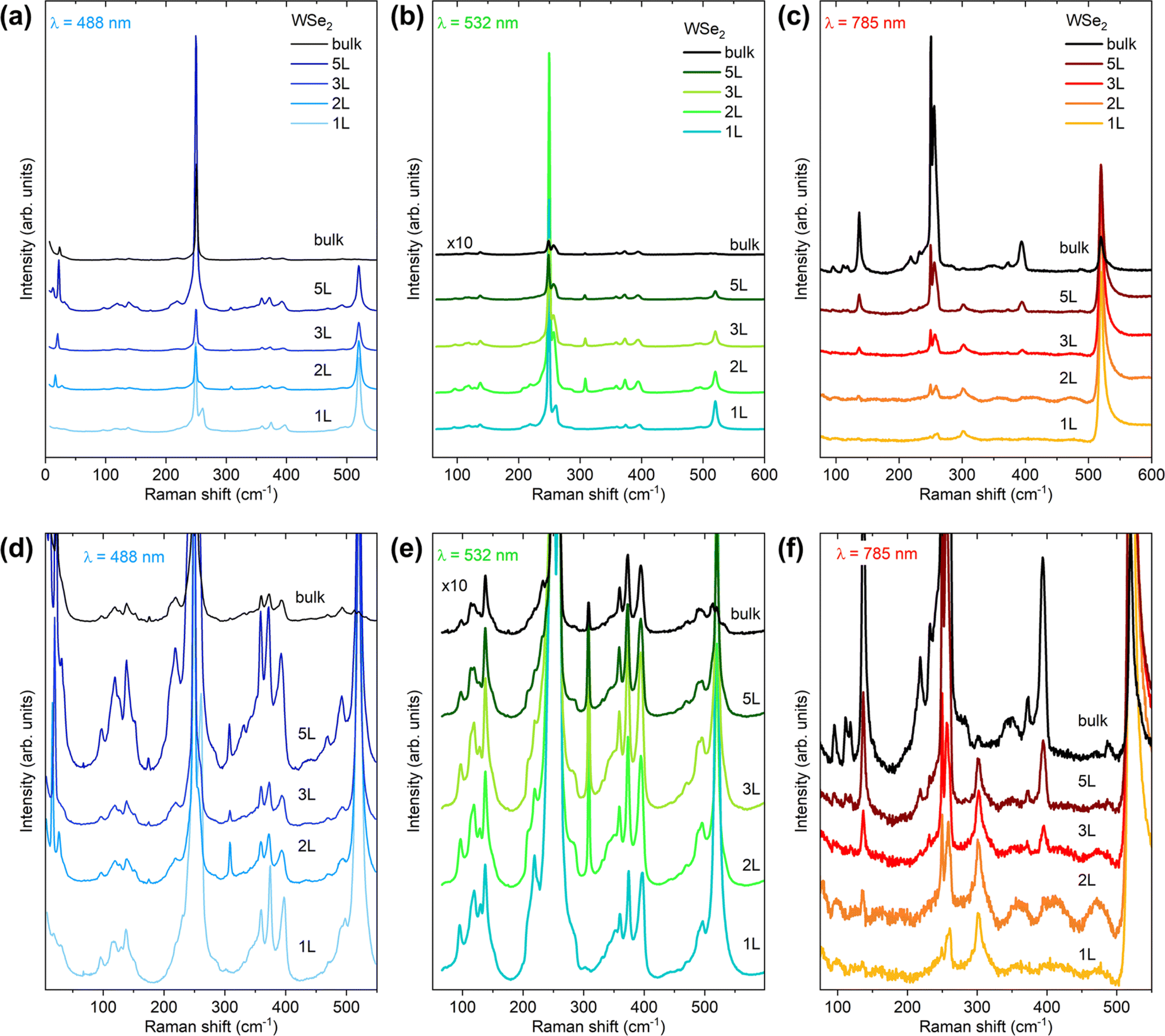 | ||
| Fig. 3 Raman spectra of 1–5L and bulk WSe2 measured with (a and d) 488 nm, (b and e) 532 nm and (c and f) 785 nm wavelength excitations. The top panel (a–c) presents the Raman spectra at the absolute intensity scale, while the bottom panel (d–f) presents a magnified intensity scale, allowing observation of low intensity Raman active peaks. The measurements were performed at room temperature and under the same acquisition conditions per excitation wavelength, allowing direct comparison of the Raman intensity among the different numbers of WSe2 layers. | ||
Deconvolution of the Raman spectra measured with 488, 532 and 785 nm excitation for each individual layer system of WSe2 was performed using the minimum number of Lorentzian components, allowing the identification of around 35 Raman peaks for each system. The representative deconvolution results corresponding to Raman spectra of 2L WSe2 measured at 488 nm, 3L WSe2 measured at 532 nm and 5L WSe2 measured at 785 nm are shown in Fig. 4a–c. Each peak was modeled with a Lorentzian curve characterized by peak position, peak width, and intensity. As the fitting procedure includes a large number of variables, rigorous restrictions were imposed on the fitting parameters in order to avoid correlation among the parameters and obtain meaningful results, as explained here below and in ref. 36,46–48. This includes leaving the intensity and peak position as free parameters, while the widths of peaks were restricted. As the peak widths are mostly dependent on the phonon lifetime, which is determined by the crystal quality of the material, it is expected that all fundamental one-phonon Raman modes have similar widths, regardless of the symmetry of the mode. This results in allowing only a narrow interval of change for the one-phonon peak widths during the deconvolution process. Possible two-phonon or multi-phonon modes are similarly modeled with higher widths compared to the one-phonon modes. This allows unambiguous interpretation of the phonon nature of the peaks, rendering the identification procedure more accurate.
 | ||
| Fig. 4 Lorentzian deconvolution of the Raman spectra for (a) 2L WSe2 measured at 488 nm, (b) 3L WSe2 measured at 532 nm and (c) 5L WSe2 measured at 785 nm excitation wavelengths. | ||
The Raman frequencies of all peaks obtained from the deconvolution process are listed in Table 1, along with their symmetry assignment and a comparison with the frequency of the DFT calculated phonon modes and experimentally reported values from the literature. All peaks are identified as either one-phonon or multi-phonon modes based on the results from the deconvolution procedure. Overall, we observe excellent agreement (on-average 2% difference) between the experimentally observed peaks and the theoretically predicted Raman frequencies. Minor disagreement in the Raman peak positions between the experimental and the theoretical results is expected, due to approximations applied during the calculations, such as the three-body and long-range interactions.
| This work | Literature | |||||||
|---|---|---|---|---|---|---|---|---|
| λ ext (nm) | ν exp (cm−1) | Symmetry assignment | ν theory (cm−1) | ν exp (cm−1) | ||||
| 1L | 2L | 3L | 5L | Bulk | ||||
| a Labels: λext – laser excitation under which the Raman mode is present; νexp – Raman peak frequency experimentally determined from the Raman spectra; νtheory – theoretically calculated Raman mode frequency; “ – ” Raman peak not observed in the spectra; “/” – additional phonon mode assignment for the Raman peak with the same frequency. Fundamental one-phonon Raman modes arising from the Γ point are highlighted in bold. | ||||||||
| 488 | — | 28 | 19 | 13 | — |
A
1g
(even),
 , and B2g(bulk)
 |
27.7 (2L), 19.4 (3L), and 14.8 (5L)43 | 28 (2L), 19 (3L), and 12 (5L)43 |
| 488 | — | 17 | 21 | 22 | 24 | E g (even), E′ (odd), and E2g(bulk) | 17.8 (2L), 21.6 (3L), 23.5 (5L), and 24.6 (bulk)43 | 17 (2L), 21 (3L), 23 (5L), and 24 (bulk)43 |
| 488 | — | — | — | 32 | — |
|
30.7 (5L)43 | 32 (5L)43 |
| 488 | 32 | 36 | 36 | 36 | 35 | LA(M) – TA(M) | 31.7 (ref. 33) | — |
| 488 | 75 | 75 | 75 | 75 | 75 | ZO2(M)–TO1(M) | 76.3 (ref. 33) | 74.4 (ref. 33) |
| All | 97 | 97 | 97 | 97 | 97 | LO1(M)–ZA(M)/TO1(M)–TA(M) | 94.2/95.3 (ref. 33) | 96.0 (ref. 33) |
| All | 115 | 114 | 114 | 111 | 111 | TO2(K)–TA(K)/ZO1(K)–LA(K)/LO2(M)–LA(M)/LO1(K)–TA(K)/LO2(K)–LA(K) | 114.5/114.9/115.1/116.3/116.5 (ref. 33) | 114.3 (ref. 33) |
| All | 119 | 119 | 119 | 119 | 119 | ZO2(K)–LA(K) | 119.5 (ref. 33) | 120.1 (ref. 33) |
| All | 128 | 128 | 128 | 127 | 127 | TO2(M)–TA(M) | 130.7 (ref. 33) | 130.5 (ref. 33) |
| All | 138 | 138 | 138 | 138 | 138 | LO2(K)–ZA(K)/ZO1(Γ)–TO/LO1(Γ) | 135.2/136.2 (ref. 33) | 137.4 (ref. 33) |
| 488, 532 | 147 | 147 | 147 | 147 | 147 | LO2(M)–TA(M) | 146.8 (ref. 33) | 145.0 (ref. 33) |
| All | 153 | 153 | 153 | 153 | 153 | ZO1(K)–TA(K) | 157.4 (ref. 33) | 158.4 (ref. 33) |
| 488, 532 | — | 176 | 175 | 175 | 176 | E g (even), E′ (odd), and E1g(bulk) | 176.3 (2L)27 | 176.3 (2L)27 |
| 488, 532 | 209 | 209 | 209 | 209 | 209 | 3- Or 4-phonon mode (example: TO2(M)–TA(M) + ZO2(M)–TO1(M)) | 209.6 (ref. 33) | 208.1 (ref. 33) |
| All | 219 | 219 | 219 | 218 | 219 | TA(M) + ZA(M) | 220.4 (ref. 33) | 219.2 (ref. 33) |
| 532, 785 | 229 | 229 | 229 | 232 | 232 | TA(M) + LA(M) | 228.5 (ref. 33) | 231.2 (ref. 33) |
| All | 240 | 240 | 240 | 241 | 241 | TA(K) + LA(K) | 242.3 (ref. 33) | 239.9 (ref. 33) |
| All | 250 | 250 | 250 | 250 | 250 |
E
g
& A
1g
(even), E′ &
 , and E2g& A1g(bulk)
 |
250.8 & 251.3 (ref. 33) | 249.9 (ref. 33) |
| All | 258 | 258 | 258 | 257 | 257 | 2vHs | 256 (ref. 33) | 258.7 (ref. 34) |
| All | 261 | 261 | 261 | 261 | 261 | 2LA(M) | 260.2 (ref. 33) | 261.0 (ref. 33) |
| 488, 532 | 283 | 283 | 284 | 284 | 284 | 2LA(K) | 284.8 (ref. 33) | 274.1 (ref. 34) |
| All | — | 309 | 309 | 309 | 309 |
A
1g
(even),
 , and B2g(bulk)
 |
311.3 (ref. 27) | 310 (ref. 27) |
| 488, 532 | 331 | 330 | 330 | 331 | 331 | TO1(K) + ZA(K) | 333.3 (ref. 33) | 331.3 (ref. 33) |
| 488, 532 | 340 | 341 | 341 | 341 | 341 | TO2(M) + ZA(M) | 339.9 (ref. 33) | 341.5 (ref. 33) |
| All | 351 | 350 | 350 | 352 | 352 | 2![[thin space (1/6-em)]](https://www.rsc.org/images/entities/char_2009.gif) TO/LO1(Γ) TO/LO1(Γ) |
352.3 (ref. 33) | 351.2 (ref. 33) |
| 488, 532 | 359 | 359 | 359 | 359 | 359 | ZO1(M) + TA(M)/ZO2(K) + TA(K) | 361.7/361.8 (ref. 33) | 360.0 (ref. 33) |
| All | 374 | 373 | 373 | 373 | 373 | LO2(M) + LA(M) | 373.3 (ref. 33) | 375.4 (ref. 33) |
| All | 396 | 394 | 394 | 394 | 394 | ZO2(M) + ZA(M) | 392.0 (ref. 33) | 393.0 (ref. 33) |
| 532 | 444 | 444 | 444 | — | — | LO1(M) + TO2(M) |
445.3 (ref. 33) | — |
| 488, 532 | 456 | 456 | 456 | 456 | 456 | TO1(M) + ZO1(M)/2TO2(M)/LO2(M) + TO2(M) |
457.0/458.2/461.4 (ref. 33) | — |
| 488, 532 | 469 | 469 | 469 | 469 | 469 | TO1(K) + ZO2(K)/TO2(K) + ZO1(K) | 471.5/471.7 (ref. 33) | — |
| All | 488 | 488 | 488 | 488 | 488 | LO1(Γ) + ZO1(Γ)/ZO1(M) + TO2(M) | 488.29/492.4 (ref. 33) | 491.3 (ref. 33) |
| 488, 532 | 496 | 496 | 496 | 496 | 496 | ZO2(M) + TO2(M) | 499.1 (ref. 33) | 499.2 (ref. 33) |
| 488, 532 | 510 | 511 | 511 | 512 | 512 | ZO1(M) + LO2(M)/2ZO1(K) | 508.5/514.6 (ref. 33) | 507.1/514.4 (ref. 33) |
| All | 533 | 532 | 532 | 532 | 532 | ZO1(M) + ZO2(M) | 533.3 (ref. 33) | 533.8 (ref. 33) |
First-order Raman modes in multilayer and bulk WSe2
First, we focus on the identification of the fundamental, one-phonon modes arising from the Γ point as the result of first-order Raman scattering. For convenience, in the text, we use the symmetry notation of bulk WSe2, while the corresponding symmetry mode labeling for different numbers of layers is presented in Table 1. One-phonon Raman peaks are located at around 10–35, ∼176, ∼250, and ∼309 cm−1. The peak at 250 cm−1 is the most intense peak in WSe2 systems, present for all numbers of layers and corresponds to the overlapped E2g and A1g phonons. Although the energies of these phonons are not degenerate (see theoretical values in Table 1), the two peaks cannot be distinguished as their energy difference is below the resolution limit of the setup. The peaks at 176 and 309 cm−1 are identified as E1g and B2g modes, respectively, and are present for all thicknesses, except for the monolayer. No change in the frequency of all the above mentioned peaks for different numbers of layers is observed within the resolution of our Raman measurements (<2 cm−1). This is in agreement with the DFT and previous experimental reports.25,27–29,33,34,43–45 Next, several low Raman intensity peaks can be observed in the region from 10 to 35 cm−1. These peaks are identified as interlayer breathing and shear modes with B2g or E2g symmetries and frequencies depending on the number of layers.43 These modes are a consequence of the interlayer van der Waals (vdW) coupling between the layers and are therefore not present in the case of monolayer WSe2.Second/higher-order Raman modes in multilayer and bulk WSe2
The other peaks present in the Raman spectra of WSe2 systems are identified as two-phonon modes from second-order Raman scattering. These modes arise from the combination of two phonons at the Γ, M or K points of the Brillouin zone, whose total momentum is zero. The combination modes have been identified based on the frequencies of the individual phonons, calculated from the DFT obtained phonon dispersions for 1L to 3L WSe2, presented in ref. 33. Overall, there is a very good agreement between the theoretically predicted and experimentally observed frequencies of modes in all cases (Table 1), except for the peak at 209 cm−1. This peak was previously identified as a single phonon mode arising from the K point of the TO1 phonon branch.33 However, activation of one-phonon modes away from the Γ point in the Brillouin zone (such as M and K points) requires the presence of a defect, which will nullify the momentum of the phonon, therefore preserving the total momentum conservation law. As this mode appears in the Raman spectra of all layer systems, including the bulk, it would mean that there is a systematic structural defect present in the lattice of WSe2 regardless of the number of layers or position on the flake. While this could not be completely excluded, a more probable process, such as multiphoton scattering should also be considered. Based on the low intensity of this peak, we believe that it might be arising from a multi Raman scattering process involving three or more phonons, such as TO2(M) − TA(M) + ZO2(M) − TO1(M). We also assign the peak at 258 cm−1 to the scattering of two phonons due to a van Hove singularity (vHs)34,49,50 at the saddle-point in the phonon density of states, located between the K and M points of the LA phonon branch (Fig. S2 in the ESI†) and labeled as 2vHs in Table 1.Finally, we note the appearance of three peaks at 302, 432 and 520 cm−1 in the Raman spectra of all WSe2 systems. These peaks arise from the oxidized Si substrate, as shown in the Raman spectra of the bare substrate in Fig. S3(a) in the ESI.† The peak at 302 cm−1 should be especially mentioned, as it has been previously attributed to WSe2,30 and explained as experiencing Breit–Wigner–Fano (BWF) type resonance for Raman measurements with 785 nm excitation. We disagree with this explanation as (1) there is no theoretically predicted one-phonon or multi-phonon mode of WSe2 at this frequency, (2) the Raman intensity of this peak scales exactly the same as the Raman intensity of the bulk Si 520 cm−1 peak (Fig. S3(b) in the ESI†), and (3) no other Raman modes of WSe2, especially fundamental one-phonon modes, experience BWF resonance for measurements with 785 nm, which makes it highly unlikely that only the 302 cm−1 mode would have such behavior. In conclusion, we attribute the Raman peak at 302 cm−1 to the TA phonon of Si and not to WSe2.
Intensity amplification in Raman scattering of multilayer and bulk WSe2
The variation of the excitation wavelength in Raman scattering provides a path to correlate the phonon with the energy band structure of the material. The identification of wavelengths maximizing the scattered intensity, also known as resonant, enables measurements with minimum excitation intensity. While our study does not include a fully tunable laser, we use multiple wavelengths. Some conditions result in a significant increase in the scattered intensity, which we relate to the band structure of our material. In order to understand the potential appearance of amplification conditions when using different excitation wavelengths, room-temperature photoluminescence (PL) measurements have been performed on the multilayer WSe2 using a 488 nm excitation wavelength, as shown in Fig. 5a. Overall, a total of four PL contributions are observed in the PL spectra of 1–5L WSe2. These have been attributed to the indirect bandgap at around 1.4 eV (2L–5L systems only), the A exciton at around 1.65 (1L), the B exciton at around 2.1 eV (1L) and the A′ exciton at 2.4 eV (1L). A, B and A′ excitons shift to lower energies with the increase in the flake thickness from 1L to 5L, as shown in Fig. 5b. Fig. 5b also plots the position of the B′ exciton obtained from the absorption measurements reported in ref. 51, which is not accessible to our PL measurements. A detailed explanation of the origin of these excitonic states was reported in several studies25,52–57 and it is not the focus of this work. | ||
| Fig. 5 Exciton energies of WSe2 and Raman resonance. (a) Room-temperature photoluminescence spectra of 1L–5L of WSe2 measured at 488 nm excitation wavelength. (b) Exciton energies in 1L–5L WSe2 determined from the PL peak positions corresponding to the indirect band gap, A, B, A′ and B′ excitons. It should be noted that the energy values of the B′ exciton have been taken from ref. 51. Energies of the laser excitations used for the Raman measurements are indicated with horizontal lines labeled 488, 532 and 785 nm. (c) Comparison of the Raman intensity of the 250 cm−1 peak with the energy difference between WSe2 excitons and laser excitation, allowing identification of Raman resonance conditions for certain WSe2 flake thicknesses. | ||
The comparison of the Raman scattering intensity of the A1g/E2g mode located at 250 cm−1 with the energy difference between a certain exciton and laser excitation is plotted in Fig. 5c. In the case of the 488 nm laser excitation, we can observe that the Raman intensity of the A1g/E2g mode is high for 1L, decreases for 2L and 3L and again increases for 5L WSe2. Considering the band structure of WSe2, amplification effects due to allowed electronic transitions are observed in the case of 1L. They are due to the coupling with the A′ exciton, and in the case of 5L, due to coupling with the B′ exciton, as shown by the line indicating the laser energy in Fig. 5b. For Raman measurements performed with 532 nm excitation, the highest intensity of the A1g/E2g mode is observed in the case of 2L WSe2. This is followed by slightly lower intensities for 1L and 3L and the lowest intensity for 5L WSe2. The Raman amplification in this case is due to coupling with the A′ exciton, whose energy in the case of 2L WSe2 (2.32 eV) ideally coincides with the green laser excitation (2.34 eV). Finally, the Raman amplification in the case of 785 nm laser excitation is observed for 5L WSe2, as the intensity of the A1g/E2g mode is the highest in comparison to the other thicknesses. The Raman amplification in this case is due to coupling with the A exciton, whose energy for 5L WSe2 is around 1.59 eV, which is very close to the energy of the red laser excitation (1.58 eV). This implies that further Raman characterization, where, for example phonon–phonon or electron–phonon interactions would be investigated, would be best achieved when using 488 nm excitation for 1L and 3L, 532 nm excitation in the case of 2L and 785 nm excitation for 5L and higher WSe2 thicknesses.
Phonon cascades in multilayer and bulk WSe2
We now turn to the low wavenumber domain of the Raman spectra, which contains information on phonon cascade processes. Phonon cascade processes occur in the first stages of carrier recombination. They are particularly fast in TMDs, rendering pump-probe experiments challenging.58 In this sense, Raman spectroscopy close to the Rayleigh line provides relevant information on these processes. A fundamental understanding and characterization of these processes is key for their application in optoelectronics.Fig. 6a and b present the Raman spectra of 1L and 5L WSe2 respectively, measured with 488 and 532 nm excitations, along with the phonon cascade fits. We attribute these peaks to phonon cascades (PCs) in the Raman spectra of 1L–5L and bulk WSe2. These oscillations are not present under 795 nm excitation, as can be clearly seen in Fig. 3f, upon comparison with Fig. 3c and d. We have fit the spectra with three periodic Gaussian peaks, labeled as NPC = 1, 2 and 3, at about 16, 31 and 46 meV, respectively. Fittings of Raman spectra for 2L and 3L layers are presented in Fig. S4 in the ESI.†
 | ||
| Fig. 6 Phonon cascades in WSe2: Raman spectra of (a) 1L and (b) 5L WSe2 measured with 488 and 532 nm laser excitations, with phonon cascade fit (labeled as PC Fit) revealing 3 periodic Gaussian peaks, labeled as NPC = 1, 2 and 3, at about 16, 31 and 46 meV, respectively. (c) Schematic illustration of the phonon cascade process. (d) Emission energies of PC peaks as a function of the number of steps in the cascade obtained from the PC fitting of the Raman spectra of 1L–5L WSe2 measured with laser excitations of 488 and 532 nm. | ||
Phonon cascades59,60 are due to the electron–phonon interaction, where electrons undergo phonon-induced transitions with a radiative recombination at each step, as illustrated in Fig. 6c. Phonon cascades start when incoming photons with energy (Eexc) excite electrons from the valence band to energy states corresponding to the in-plane wavevector cone of k ≤ ωexc/c, where ωexc is the frequency of the incoming photons (this cone is indicated with blue dashed lines in Fig. 6c). Due to phonon–electron interaction, the excited electrons undergo successive transitions between vibrational states (labeled with dashed black lines in Fig. 6c). At each step, one phonon with an energy corresponding to the difference between the vibrational states (Ephonon) is created. The creation of phonons is followed by a possible radiative recombination of the electron with the hole in the valence band and emission of a photon with an energy Eexc – NPCEphonon, where NPC corresponds to the number of phonons that were created in the phonon cascade process. As a result, periodic emission peaks are observed in the energy region close to the laser excitation (i.e. the Raman region, also called the hot photoluminescence region). According to the theory,61 similar behavior of phonon cascades is expected for involvement of excitons, as well as for free electrons or holes. Therefore, it is not possible to distinguish between free-carrier and exciton cascades from hot photoluminescence experiments. However, considering that excitonic behavior is dominant in WSe2, it makes sense that phonon cascades involving excitons are more probable.
The excitation energy of the incoming photons needs to be above the free-carrier gap excitation for phonon cascades to occur. This is the reason why phonon cascades in WSe2 are not observed with 785 nm laser excitation, as the energy of the A exciton for 1L–5L WSe2 is always higher than the 785 nm laser energy (1.58 eV), which in turn is insufficient to excite the carriers above the A exciton level.
Previously, phonon cascades were reported only in monolayer WSe2.62 Here, we report phonon cascades up to 5L and bulk WSe2. While the fine structure of the spectra is slightly different as a function of the number of ML, PC fitting did not reveal any significant shift in the energy of the PC peaks with the change in the WSe2 layer thickness, or with the change in the laser excitation, as indicated in Fig. 5d. Linear fitting of the PC peak energy (EPC) with the number of peaks in the cascade (NPC), allows for the determination of the energy of the phonon (Ephonon) involved in the cascade process, as shown in Fig. 5d. This also corresponds to the average energy difference between successive PC peaks. In this case, the obtained phonon energy of around 15.4 meV is in agreement with the reports for monolayer WSe2.62 This energy corresponds well to the out-of-plane (ZA) acoustic phonon (around 125 cm−1) at the M and K points of the Brillouin zone (Fig. S2 in the ESI†). The involvement of the ZA phonon is further confirmed by its phonon branch being relatively flat in the region between the M and K points, which is necessary for the generation of a high number of PC peaks.
The observation of phonon cascades in WSe2 indicates that an exceptionally strong electron–phonon interaction occurs in the initial steps of carrier relaxation that prevails until 5ML, which may provide design-relevant insights for emerging optoelectronic applications.
Conclusions
We present a complete investigation of the vibrational properties of 1L to 5L and bulk WSe2 using multiwavelength excitation Raman spectroscopy. The systematic deconvolution and comprehensive analysis of Raman spectra across different excitation energies enabled the reliable identification of 35 Raman peaks for each flake thickness, which were attributed to either one-phonon or two-phonon modes. The results are in agreement with the theoretical predictions. Furthermore, we have resolved inconsistencies in the literature in terms of activation of non-Γ point single phonon modes and BWF type resonance. Using photoluminescence measurements, we identify photon-exciton coupling leading to strong enhancement in Raman intensity. Based on this, we suggest optimal laser excitations best suited for further Raman investigations of specific WSe2 layer thicknesses. Finally, we report the observation of phonon-cascades involving ZA phonons for all WSe2 layer thicknesses, indicating strong phonon–electron interactions during early carrier relaxation processes. This research provides a solid foundation and reference for further investigations of the vibrational properties of WSe2, paving the way for WSe2 integration into advanced optoelectronic and phononic devices.Data availabitlity
The data for this article are available at https://doi.org/10.5281/zenodo.12696856.Author contributions
M. D. and A. F. iM. conceived the research idea and supervised the work. C. B. performed the Raman and AFM measurements. A. B. prepared the sample under supervision of M. B. M. D. performed the PL measurements. C. B., A. L. and M. D. analyzed the data. M. D. and C. B. wrote the manuscript with inputs from all co-authors.Conflicts of interest
The authors declare that they have no competing financial interests.Acknowledgements
A. F. iM, C. B. and A. B. acknowledge funding from the Swiss National Science Foundation under the grant number 200021_196948. M.B. acknowledges the support of SNSF Eccellenza grant No. PCEGP2_194528, and support from the QuantERA II Programme that has received funding from the European Union's Horizon 2020 research and innovation program under Grant Agreement No. 101017733.References
- G. Wang, A. Chernikov, M. M. Glazov, T. F. Heinz, X. Marie, T. Amand and B. Urbaszek, Colloquium: excitons in atomically thin transition metal dichalcogenides, Rev. Mod. Phys., 2018, 90, 021001 CrossRef CAS.
- K. F. Mak and J. Shan, Photonics and optoelectronics of 2D semiconductor transition metal dichalcogenides, Nat. Photon., 2016, 10, 216–226 CrossRef CAS.
- T. Mueller and E. Malic, Exciton physics and device application of two-dimensional transition metal dichalcogenide semiconductors, NPJ 2D Mater. Appl., 2018, 2, 1–12 CrossRef CAS.
- J. R. Schaibley, H. Yu, G. Clark, P. Rivera, J. S. Ross, K. L. Seyler, W. Yao and X. Xu, Valleytronics in 2D materials, Nat. Rev. Mater., 2016, 1, 1–15 Search PubMed.
- L. Sortino, P. G. Zotev, C. L. Phillips, A. J. Brash, J. Cambiasso, E. Marensi, A. M. Fox, S. A. Maier, R. Sapienza and A. I. Tartakovskii, Bright single photon emitters with enhanced quantum efficiency in a two-dimensional semiconductor coupled with dielectric nano-antennas, Nat. Commun., 2021, 12, 6063 CrossRef CAS PubMed.
- P. Norouzzadeh and D. J. Singh, Thermal conductivity of single-layer WSe2 by a Stillinger–Weber potential, Nanotechnology, 2017, 28, 075708 CrossRef PubMed.
- P. Torres, F. X. Alvarez, X. Cartoixà and R. Rurali, Thermal conductivity and phonon hydrodynamics in transition metal dichalcogenides from first-principles, 2D Mater., 2019, 6, 035002 CrossRef CAS.
- M. Zulfiqar, Y. Zhao, G. Li, Z. Li and J. Ni, Intrinsic thermal conductivities of monolayer transition metal dichalcogenides MX2 (M = Mo, W; X = S, Se, Te), Sci. Rep., 2019, 9, 4571 CrossRef PubMed.
- Q. Zheng, Y. Xie, Z. Lan, O. V. Prezhdo, W. A. Saidi and J. Zhao, Phonon-coupled ultrafast interlayer charge oscillation at van der Waals heterostructure interfaces, Phys. Rev. B, 2018, 97, 205417 CrossRef CAS.
- C. M. Chow, H. Yu, A. M. Jones, J. Yan, D. G. Mandrus, T. Taniguchi, K. Watanabe, W. Yao and X. Xu, Unusual exciton–phonon interactions at van der waals engineered interfaces, Nano Lett., 2017, 17, 1194–1199 CrossRef CAS PubMed.
- M.-L. Lin, Q.-H. Tan, J.-B. Wu, X.-S. Chen, J.-H. Wang, Y.-H. Pan, X. Zhang, X. Cong, J. Zhang, W. Ji, P.-A. Hu, K.-H. Liu and P.-H. Tan, Moiré Phonons in twisted bilayer MoS2, ACS Nano, 2018, 12, 8770–8780 CrossRef CAS PubMed.
- G. B. Barin, A. Fairbrother, L. Rotach, M. Bayle, M. Paillet, L. Liang, V. Meunier, R. Hauert, T. Dumslaff, A. Narita, K. Müllen, H. Sahabudeen, R. Berger, X. Feng, R. Fasel and P. Ruffieux, Surface-synthesized graphene nanoribbons for room-temperature switching devices: substrate transfer and ex-situ characterization, ACS Appl. Nano Mater., 2019, 2(4), 2184–2192 CrossRef.
- I. A. Verzhbitskiy, M. D. Corato, A. Ruini, E. Molinari, A. Narita, Y. Hu, M. G. Schwab, M. Bruna, D. Yoon, S. Milana, X. Feng, K. Müllen, A. C. Ferrari, C. Casiraghi and D. Prezzi, Raman fingerprints of atomically precise graphene nanoribbons, Nano Lett., 2016, 16, 3442–3447 CrossRef CAS PubMed.
- L. G. Cançado, A. Jorio, E. H. M. Ferreira, F. Stavale, C. A. Achete, R. B. Capaz, M. V. O. Moutinho, A. Lombardo, T. S. Kulmala and A. C. Ferrari, Quantifying defects in graphene via raman spectroscopy at different excitation energies, Nano Lett., 2011, 11, 3190–3196 CrossRef PubMed.
- M. M. Lucchese, F. Stavale, E. H. M. Ferreira, C. Vilani, M. V. O. Moutinho, R. B. Capaz, C. A. Achete and A. Jorio, Quantifying ion-induced defects and Raman relaxation length in graphene, Carbon, 2010, 48, 1592–1597 CrossRef CAS.
- C. Neumann, S. Reichardt, P. Venezuela, M. Drögeler, L. Banszerus, M. Schmitz, K. Watanabe, T. Taniguchi, F. Mauri, B. Beschoten, S. V. Rotkin and C. Stampfer, Raman spectroscopy as probe of nanometre-scale strain variations in graphene, Nat. Commun., 2015, 6, 8429 CrossRef CAS PubMed.
- L. Banszerus, H. Janssen, M. Otto, A. Epping, T. Taniguchi, K. Watanabe, B. Beschoten, D. Neumaier and C. Stampfer, Identifying suitable substrates for high-quality graphene-based heterostructures, 2D Mater., 2017, 4, 025030 CrossRef.
- O. Frank, M. Mohr, J. Maultzsch, C. Thomsen, I. Riaz, R. Jalil, K. S. Novoselov, G. Tsoukleri, J. Parthenios, K. Papagelis, L. Kavan and C. Galiotis, Raman 2D-band splitting in graphene: theory and experiment, ACS Nano, 2011, 5, 2231–2239 CrossRef CAS PubMed.
- J. E. Lee, G. Ahn, J. Shim, Y. S. Lee and S. Ryu, Optical separation of mechanical strain from charge doping in graphene, Nat. Commun., 2012, 3, 1024 CrossRef PubMed.
- C. Stampfer, F. Molitor, D. Graf, K. Ensslin, A. Jungen, C. Hierold and L. Wirtz, Raman imaging of doping domains in graphene on SiO2, Appl. Phys. Lett., 2007, 91, 241907 CrossRef.
- N. J. G. Couto, D. Costanzo, S. Engels, D.-K. Ki, K. Watanabe, T. Taniguchi, C. Stampfer, F. Guinea and A. F. Morpurgo, Random strain fluctuations as dominant disorder source for high-quality on-substrate graphene devices, Phys. Rev. X, 2014, 4, 041019 CAS.
- G. Froehlicher and S. Berciaud, Raman spectroscopy of electrochemically gated graphene transistors: geometrical capacitance, electron-phonon, electron-electron, and electron-defect scattering, Phys. Rev. B: Condens. Matter Mater. Phys., 2015, 91, 205413 CrossRef.
- J. Sonntag, K. Watanabe, T. Taniguchi, B. Beschoten and C. Stampfer, Charge carrier density dependent Raman spectra of graphene encapsulated in hexagonal boron nitride, Phys. Rev. B, 2023, 107, 075420 CrossRef CAS.
- X. Zhang, X.-F. Qiao, W. Shi, J.-B. Wu, D.-S. Jiang and P.-H. Tan, Phonon and Raman scattering of two-dimensional transition metal dichalcogenides from monolayer, multilayer to bulk material, Chem. Soc. Rev., 2015, 44, 2757–2785 RSC.
- E. del Corro, H. Terrones, A. Elias, C. Fantini, S. Feng, M. A. Nguyen, T. E. Mallouk, M. Terrones and M. A. Pimenta, Excited excitonic states in 1L, 2L, 3L, and bulk WSe2 observed by resonant raman spectroscopy, ACS Nano, 2014, 8, 9629–9635 CrossRef CAS PubMed.
- W. Zhao, Z. Ghorannevis, K. K. Amara, J. R. Pang, M. Toh, X. Zhang, C. Kloc, P. H. Tan and G. Eda, Lattice dynamics in mono- and few-layer sheets of WS2 and WSe2, Nanoscale, 2013, 5, 9677–9683 RSC.
- X. Luo, Y. Zhao, J. Zhang, M. Toh, C. Kloc, Q. Xiong and S. Y. Quek, Effects of lower symmetry and dimensionality on Raman spectra in two-dimensional WSe2, Phys. Rev. B: Condens. Matter Mater. Phys., 2013, 88, 195313 CrossRef.
- H. Terrones, E. D. Corro, S. Feng, J. M. Poumirol, D. Rhodes, D. Smirnov, N. R. Pradhan, Z. Lin, M. a. T. Nguyen, A. L. Elías, T. E. Mallouk, L. Balicas, M. A. Pimenta and M. Terrones, New first order raman-active modes in few layered transition metal dichalcogenides, Sci. Rep., 2014, 4, 4215 CrossRef CAS PubMed.
- W. Shi, M.-L. Lin, Q.-H. Tan, X.-F. Qiao, J. Zhang and P.-H. Tan, Raman and photoluminescence spectra of two-dimensional nanocrystallites of monolayer WS2 and WSe2, 2D Mater., 2016, 3, 025016 CrossRef.
- S. Kim, K. Kim, J.-U. Lee and H. Cheong, Excitonic resonance effects and Davydov splitting in circularly polarized Raman spectra of few-layer WSe2, 2D Mater., 2017, 4, 045002 CrossRef.
- S. M. Eichfeld, L. Hossain, Y.-C. Lin, A. F. Piasecki, B. Kupp, A. G. Birdwell, R. A. Burke, N. Lu, X. Peng, J. Li, A. Azcatl, S. McDonnell, R. M. Wallace, M. J. Kim, T. S. Mayer, J. M. Redwing and J. A. Robinson, Highly scalable, atomically thin WSe2 grown via metal–organic chemical vapor deposition, ACS Nano, 2015, 9, 2080–2087 CrossRef CAS PubMed.
- Y. Gong, Q. Zhou, X. Huang, B. Han, X. Fu, H. Gao, F. Li and T. Cui, Pressure-induced photoluminescence adjustment and lattice disorder in monolayer WSe2, ChemNanoMat, 2017, 3, 238–244 CrossRef CAS.
- M. D. Luca, X. Cartoixà, J. Martín-Sánchez, M. López-Suárez, R. Trotta, R. Rurali and I. Zardo, New insights in the lattice dynamics of monolayers, bilayers, and trilayers of WSe2 and unambiguous determination of few-layer-flakes’ thickness, 2D Mater., 2020, 7, 025004 CrossRef.
- L. G. Pimenta Martins, B. R. Carvalho, C. A. Occhialini, N. P. Neme, J.-H. Park, Q. Song, P. Venezuela, M. S. C. Mazzoni, M. J. S. Matos, J. Kong and R. Comin, Electronic band tuning and multivalley raman scattering in monolayer transition metal dichalcogenides at high pressures, ACS Nano, 2022, 16, 8064–8075 CrossRef CAS PubMed.
- M. Dimitrievska, A. Fairbrother, A. Pérez-Rodríguez, E. Saucedo and V. Izquierdo-Roca, Raman scattering crystalline assessment of polycrystalline Cu2ZnSnS4 thin films for sustainable photovoltaic technologies: Phonon confinement model, Acta Mater., 2014, 70, 272–280 CrossRef CAS.
- M. Dimitrievska, F. Oliva, M. Guc, S. Giraldo, E. Saucedo, A. Pérez-Rodríguez and V. Izquierdo-Roca, Defect characterisation in Cu2ZnSnSe4 kesterites via resonance Raman spectroscopy and the impact on optoelectronic solar cell properties, J. Mater. Chem. A, 2019, 7, 13293–13304 RSC.
- M. Placidi, M. Dimitrievska, V. Izquierdo-Roca, X. Fontané, A. Castellanos-Gomez, A. Pérez-Tomás, N. Mestres, M. Espindola-Rodriguez, S. López-Marino, M. Neuschitzer, V. Bermudez, A. Yaremko and A. Pérez-Rodríguez, Multiwavelength excitation Raman scattering analysis of bulk and two-dimensional MoS2: vibrational properties of atomically thin MoS2 layers, 2D Mater., 2015, 2, 035006 CrossRef.
- B. R. Carvalho, Y. Wang, S. Mignuzzi, D. Roy, M. Terrones, C. Fantini, V. H. Crespi, L. M. Malard and M. A. Pimenta, Intervalley scattering by acoustic phonons in two-dimensional MoS2 revealed by double-resonance Raman spectroscopy, Nat. Commun., 2017, 8, 14670 CrossRef PubMed.
- M. Negri, L. Francaviglia, D. Dumcenco, M. Bosi, D. Kaplan, V. Swaminathan, G. Salviati, A. Kis, F. Fabbri and A. Fontcuberta i Morral, Quantitative nanoscale absorption mapping: a novel technique to probe optical absorption of two-dimensional materials, Nano Lett., 2020, 20, 567–576 CrossRef CAS PubMed.
- M. I. Aroyo, J. M. Perez-Mato, D. Orobengoa, E. Tasci, G. De La Flor and A. Kirov, Crystallography online: bilbao crystallographic server, Bulg. Chem. Commun., 2011, 43, 183–197 CAS.
- M. I. Aroyo, J. M. Perez-Mato, C. Capillas, E. Kroumova, S. Ivantchev, G. Madariaga, A. Kirov and H. Wondratschek, Bilbao crystallographic server: I. Databases and crystallographic computing programs, Z. Kristallogr. – Cryst. Mater., 2006, 221, 15–27 CrossRef CAS.
- M. I. Aroyo, A. Kirov, C. Capillas, J. M. Perez-Mato and H. Wondratschek, Bilbao Crystallographic server. II. Representations of crystallographic point groups and space groups, Acta Cryst. A, 2006, 62, 115–128 CrossRef PubMed.
- Y. Zhao, X. Luo, H. Li, J. Zhang, P. T. Araujo, C. K. Gan, J. Wu, H. Zhang, S. Y. Quek, M. S. Dresselhaus and Q. Xiong, Interlayer breathing and shear modes in few-trilayer MoS2 and WSe2, Nano Lett., 2013, 13, 1007–1015 CrossRef CAS PubMed.
- H. Sahin, S. Tongay, S. Horzum, W. Fan, J. Zhou, J. Li, J. Wu and F. M. Peeters, Anomalous Raman spectra and thickness-dependent electronic properties of WSe2, Phys. Rev. B: Condens. Matter Mater. Phys., 2013, 87, 165409 CrossRef.
- G. S. Papanai and B. K. Gupta, Spectroscopic studies on CVD-grown monolayer, bilayer, and ribbon structures of WSe2 flakes, Mater. Chem. Front., 2023, 7, 3102–3115 RSC.
- M. Dimitrievska, A. P. Litvinchuk, A. Zakutayev and A. Crovetto, Phonons in copper diphosphide (CuP2): raman spectroscopy and lattice dynamics calculations, J. Phys. Chem. C, 2023, 127, 10649–10654 CrossRef CAS PubMed.
- E. Z. Stutz, S. E. Steinvall, A. P. Litvinchuk, J.-B. Leran, M. Zamani, R. Paul, A. F. i Morral and M. Dimitrievska, Raman spectroscopy and lattice dynamics calculations of tetragonally-structured single crystal zinc phosphide (Zn3P2) nanowires, Nanotechnology, 2020, 32, 085704 CrossRef PubMed.
- M. Flór, E. Z. Stutz, S. P. Ramanandan, M. Zamani, R. Paul, J.-B. Leran, A. P. Litvinchuk, A. F. i Morral and M. Dimitrievska, Raman tensor of zinc-phosphide (Zn3P2): from polarization measurements to simulation of Raman spectra, Phys. Chem. Chem. Phys., 2022, 24, 63–72 RSC.
- J. Kürti, J. Koltai and V. Zólyomi, The role of Van Hove singularities in disorder induced Raman scattering, AIP Conf. Proc., 2005, 786, 416–419 CrossRef.
- E. Koo, S. Kim and S.-Y. Ju, Relationships between the optical and Raman behavior of van Hove singularity in twisted bi- and fewlayer graphenes and environmental effects, Carbon, 2017, 111, 238–247 CrossRef CAS.
- W. Zhao, Z. Ghorannevis, L. Chu, M. Toh, C. Kloc, P.-H. Tan and G. Eda, Evolution of Electronic structure in atomically thin sheets of WS2 and WSe2, ACS Nano, 2013, 7, 791–797 CrossRef CAS PubMed.
- R. A. Bromley, R. B. Murray and A. D. Yoffe, The band structures of some transition metal dichalcogenides. III. Group VIA: trigonal prism materials, J. Phys. C: Solid State Phys., 1972, 5, 759 CrossRef CAS.
- A. R. Beal, J. C. Knights and W. Y. Liang, Transmission spectra of some transition metal dichalcogenides. II. Group VIA: trigonal prismatic coordination, J. Phys. C: Solid State Phys., 1972, 5, 3540 CrossRef CAS.
- D. Kozawa, R. Kumar, A. Carvalho, K. Kumar Amara, W. Zhao, S. Wang, M. Toh, R. M. Ribeiro, A. H. Castro Neto, K. Matsuda and G. Eda, Photocarrier relaxation pathway in two-dimensional semiconducting transition metal dichalcogenides, Nat. Commun., 2014, 5, 4543 CrossRef CAS PubMed.
- Y. Li, A. Chernikov, X. Zhang, A. Rigosi, H. M. Hill, A. M. van der Zande, D. A. Chenet, E.-M. Shih, J. Hone and T. F. Heinz, Measurement of the optical dielectric function of monolayer transition-metal dichalcogenides: MoS2, MoSe2, WS2, WSe2, Phys. Rev. B: Condens. Matter Mater. Phys., 2014, 90, 205422 CrossRef.
- R. Schmidt, I. Niehues, R. Schneider, M. Drüppel, T. Deilmann, M. Rohlfing, S. M. de Vasconcellos, A. Castellanos-Gomez and R. Bratschitsch, Reversible uniaxial strain tuning in atomically thin WSe2, 2D Mater., 2016, 3, 021011 CrossRef.
- R. Frisenda, Y. Niu, P. Gant, A. J. Molina-Mendoza, R. Schmidt, R. Bratschitsch, J. Liu, L. Fu, D. Dumcenco, A. Kis, D. P. D. Lara and A. Castellanos-Gomez, Micro-reflectance and transmittance spectroscopy: a versatile and powerful tool to characterize 2D materials, J. Phys. D: Appl. Phys., 2017, 50, 074002 CrossRef.
- C. Robert, D. Lagarde, F. Cadiz, G. Wang, B. Lassagne, T. Amand, A. Balocchi, P. Renucci, S. Tongay, B. Urbaszek and X. Marie, Exciton radiative lifetime in transition metal dichalcogenide monolayers, Phys. Rev. B, 2016, 93, 205423 CrossRef.
- E. F. Smith and P. T. Landsberg, Phonon cascade theory, J. Phys. Chem. Solids, 1966, 27, 1727–1738 CrossRef CAS.
- P. Gilliot, C. Brimont, S. Cronenberger, O. Crégut, M. Gallart, B. Hönerlage, K. Kheng and H. Mariette, LO-phonon cascade emission in CdZnTe quantum wells: coherent control and quantum kinetics, J. Phys.: Conf. Ser., 2007, 92, 012038 CrossRef.
- R. M. Martin and C. M. Varma, Cascade theory of inelastic scattering of light, Phys. Rev. Lett., 1971, 26, 1241–1244 CrossRef CAS.
- I. Paradisanos, G. Wang, E. M. Alexeev, A. R. Cadore, X. Marie, A. C. Ferrari, M. M. Glazov and B. Urbaszek, Efficient phonon cascades in WSe2 monolayers, Nat. Commun., 2021, 12, 538 CrossRef CAS PubMed.
Footnote |
| † Electronic supplementary information (ESI) available. See DOI: https://doi.org/10.1039/d4na00399c |
| This journal is © The Royal Society of Chemistry 2024 |