
 Open Access Article
 This Open Access Article is licensed under a Creative Commons Attribution-Non Commercial 3.0 Unported Licence
Resonant tunneling in a colloidal CdS semiconductor quantum-dot single-electron transistor based on heteroepitaxial-spherical Au/Pt nanogap electrodes†
Genki
Ohkatsu
 a,
Takumi
Nishinobo
a,
Masaki
Saruyama
b,
Toshiharu
Teranishi
b and
Yutaka
Majima
*a
a,
Takumi
Nishinobo
a,
Masaki
Saruyama
b,
Toshiharu
Teranishi
b and
Yutaka
Majima
*a
aLaboratory for Materials and Structures, Institute of Innovative Research, Tokyo Institute of Technology, Yokohama 226-8503, Japan. E-mail: majima@msl.titech.ac.jp
bInstitute for Chemical Research, Kyoto University, Uji 611-0011, Japan
First published on 27th June 2024
Abstract
Semiconductor quantum dots (QDs) have unique discrete energy levels determined by the particle size and material. Therefore, they have potential applications as novel optical and electronic devices. Among those, colloidal group II–VI semiconductor quantum dots stand out for their facile synthesis and band gaps aligned with the visible light spectrum. However, the electrical characterization studies of an individual quantum dot necessitate the size of nanogap electrodes being equal to the size of the quantum dot, which has conventionally been evaluated using techniques such as scanning tunneling microscopy (STM) and nanogaps fabricated by electromigration. The complexity of device fabrication has restricted research in this area. Here, we present a pioneering approach for the electrical characterization of single-QD: heteroepitaxial-spherical (HS) Au/Pt nanogap electrodes. We fabricated transistors through chemisorption, an anchoring colloidal CdS QD (3.8 nm) between the HS-Au/Pt nanogap electrodes (gap separation: 4.5 nm). The resulting device functions as a quantum-dot single-electron transistor (QD-SET), showing resonant tunneling—an inherent characteristic of the QD. A steep current increase was observed at a negative voltage, apart from the theoretical single-electron tunneling current by Coulomb blockade phenomena, which agreed with the theoretical resonant tunneling current through a discrete energy level of the QD. This underscores the promise of HS-Au/Pt nanogap electrodes in realizing single-QD devices, offering a pathway toward unlocking their full potential.
Introduction
In a semiconductor quantum dot (QD), electron motion is confined to a 3D nanoscale volume. When the QD size decreases below a few tens of nanometers, the band gap energy widens compared to that of bulk crystals with decreasing size,1 and the energy band is discretized into different energy levels.2 The electrical properties of single-semiconductor QDs have been widely studied in Si QDs3–5 and groups III–V QDs6 and have been demonstrated through scanning tunneling microscopy7,8 and as a single-electron transistor (SET) operation.9–12Recently, group II–VI semiconductor QDs have attracted considerable attention as materials for light-emitting devices13,14 and QD solar cells.15 The advantages of group II–VI semiconductor QDs are that they can be chemically synthesized as colloidal QDs, and the band gap energy has been controlled in the near-visible light region.16 Considering that the electrical properties of single QDs strongly depend on the state of discrete energy levels, colloidal QDs are promising candidates for next-generation transistor devices because of their ability to tune discrete energy levels through precise structural control.
On a few nm scale of single semiconductor QD SETs based on double-barrier tunneling junctions, two current conduction phenomena of Coulomb blockade and resonant tunneling effects, which suppress and enhance electron tunneling, are observed, respectively. The single-electron tunneling current is suppressed by Coulomb blockade when the charging energy of the system by adding one electron on the Coulomb island is greater than the thermal energy.17,18 On the other hand, the resonant tunneling current increases when a discrete energy level of the QD is aligned with the Fermi energy of the electrode. Previously, we reported resonant tunneling phenomena on a single π-conjugate molecule with 4.5 nm in the gap separation.19
To observe the electrical properties of a single colloidal QD SET, it is necessary to place a single QD between nanogap electrodes with gap separation similar to its diameter. The width of electromigrated nanogap electrodes tends to be as wide as 100 nm,12 which is much wider than the size of QDs and makes it difficult to control the precise gap separation on a few nm scale since the gap formation occurs at electromigration points.
Recently, we have established the fabrication techniques of heteroepitaxial spherical (HS-)Au/Pt nanogap electrodes.20,21 Robust Pt nanogap electrodes with a 10 nm gap separation and a 10 nm gap width were prepared by electron-beam lithography (EBL).20 The thermal stability of the Pt nanogap electrodes is more than 773 K.20 Then, the gap separation of the Pt nanogap is decreased by the unique electroless Au-plating (ELGP) method.21,22 During ELGP, heteroepitaxial and spherical growth of Au on the Pt nanogap is obtained, and the radius of spherical Au is lower than 5 nm.21 The thermal stability of the HS-Au/Pt nanogap is higher than 573 K. We reported a single-molecule SET operation using the HS-Au/Pt nanogap electrodes.23 As the radius is smaller than 5 nm, when a few nm scale semiconductor QDs are used, only a QD could be introduced between the HS-Au/Pt nanogap electrodes, and we could discuss the energy levels of a single QD through transistor properties.
Here, we demonstrate resonant tunneling phenomena and single-electron tunneling effects by Coulomb blockade in a colloidal CdS QD SET with a chemisorbed QD between HS-Au/Pt nanogap electrodes anchored by an alkanedithiol/alkanethiol mixed self-assembled monolayer (SAM). Steep current increases were observed in the drain current (Id)–drain voltage (Vd) characteristics. The resonant tunneling phenomena are compared with the theoretical single-electron tunneling current based on the Coulomb blockade. The abrupt current reduction is discussed based on the shift of the discrete energy level of CdS QDs caused by the trapped charge around QDs, suppressing the resonant tunneling current.
Experimental
HS-Au/Pt nanogap electrodes were fabricated based on our previous reports.20,21 First, Pt initial nanogap electrodes were fabricated by EBL and lift-off. Nanogap patterns were prepared on a SiO2 (50 nm)/Si substrate using EBL. Subsequently, 3 nm of Ti and 10 nm of Pt were evaporated using an electron beam evaporator and lifted off. Contact pad electrodes were prepared using photolithography liftoff. ELGP solution was prepared by dissolving a Au sheet in medical iodine tincture (I2 and KI in ethanol), and then L(+) ascorbic acid was added as a reducing agent.21 The Pt initial nanogap electrodes with 10 nm in the gap separation and 15 nm in the gap width were immersed in the 1000 times diluted ELGP solution using deionized water for heteroepitaxial spherical gold plating, and HS-Au/Pt nanogap electrodes were fabricated.CdS QDs were synthesized based on previous reports.24 CdS QDs were protected using 1-dodecanethiol/dodecanoic acid/dodecylamine. HS-Au/Pt nanogap electrodes were immersed in a 1-decanethiol solution (TCI, 1 mM, 24 h) and then in a 1,16-hexadecanedithiol solution (Sigma-Aldrich, 1 mM, 24 h) to form a mixed SAM.25,26 The CdS QDs were chemisorbed between the mixed SAM-covered HS-Au/Pt nanogap electrodes using 1,16-hexadecanedithiol during the immersion of the CdS QD solution (36 h).
Scanning electron microscopy (SEM) and scanning transmission electron microscopy (STEM) images were recorded using field-emission SEMs (Hitachi: SU-8000 and Regulus 8230, respectively). Electrical measurements were performed using a semiconductor parameter analyzer (Keysight, B1500) and a probe station with a helium refrigerator (Nagase, GRAIL 10-LOGOS01S) in a vacuum at 9 K. The gate voltage Vg was applied from the Si substrate as the back-gate electrode.
Results and discussion
The SEM image of the CdS QD transistor based on a CdS QD and HS-Au/Pt nanogap electrodes is shown in Fig. 1(a). The gap separation was 4.5 nm, and the pair of radii of HS-Au at the gap were 4.4 and 4.8 nm. The STEM image of the CdS QDs is shown in Fig. 1(b). The average diameter of the CdS QD core and that with a ligand shell were estimated to be 3.8 ± 0.4 nm and 6.0 nm, respectively. The schematic of QD-SET with an overlayed magnified SEM image is shown at the top right of Fig. 1(a). The chemisorbed colloidal QD (6.0 nm) is placed between the gap (4.5 nm). The pair of HS-Au is also covered with the 1,16-hexadecanedithiol and 1-dodecanethiol mixed self-assembled monolayer. As a result, a single CdS QD could be introduced between the HS-Au/Pt nanogap electrodes. | ||
| Fig. 1 (a) SEM images of the colloidal CdS semiconductor QD-SET based on heteroepitaxial spherical Au/Pt nanogap electrodes. The schematic of the QD-SET overlayed on the magnified SEM image is shown at the top right. The gap separation is 4.5 nm. The chemisorbed colloidal (blue circle) QD core (yellow circle), which behaves as a Coulomb island and contributes to resonant tunneling through its discrete energy level, was placed between heteroepitaxial spherical Au/Pt nanogap electrodes. At the gap, a pair of heteroepitaxial spherical (HS)-Au (orange circles: 8.8 and 9.6 nm) are covered by a 1,16-hexadecanedithiol and 1-dodecanethiol mixed self-assembled monolayer (green circles). (b) Scanning transmission electron microscopy (STEM) image of the synthesized CdS QDs. The core diameter of CdS QDs is 3.8 ± 0.4 nm. (c) Absorption and photoluminescence spectra of CdS QDs (1.07 × 10⁻⁴ mM, n-hexane). The excitation wavelength for the PL spectrum was 350 nm. | ||
Fig. 1(c) shows the absorption and photoluminescence spectra of the CdS QDs in n-hexane. The absorption and photoluminescence peaks were at 450 and 633 nm, respectively. The bandgap energy of CdS QDs is evaluated to be 2.8 eV from the absorption peak,27 which is slightly larger than that of bulk CdS (2.4 eV). This band gap energy of CdS QDs is consistent with a previous result,28,29 suggesting a size-dependent expansion of the band gap energy and electron confinement.
The Vg dependence of the Id–Vd characteristics of the CdS QD transistor under consecutive forward and backward Vd sweeps between −0.8 and 0.8 V was measured at 9 K and is shown in Fig. 2. Due to a slightly large Vd sweep range between −0.8 and 0.8 V, the Id–Vd characteristics slightly fluctuated. However, as shown in Fig. 2, the Id–Vd characteristics under forward Vd sweep are almost equal to those under backward Vd sweep; we could discuss the Id–Vd characteristics using the experimental results.
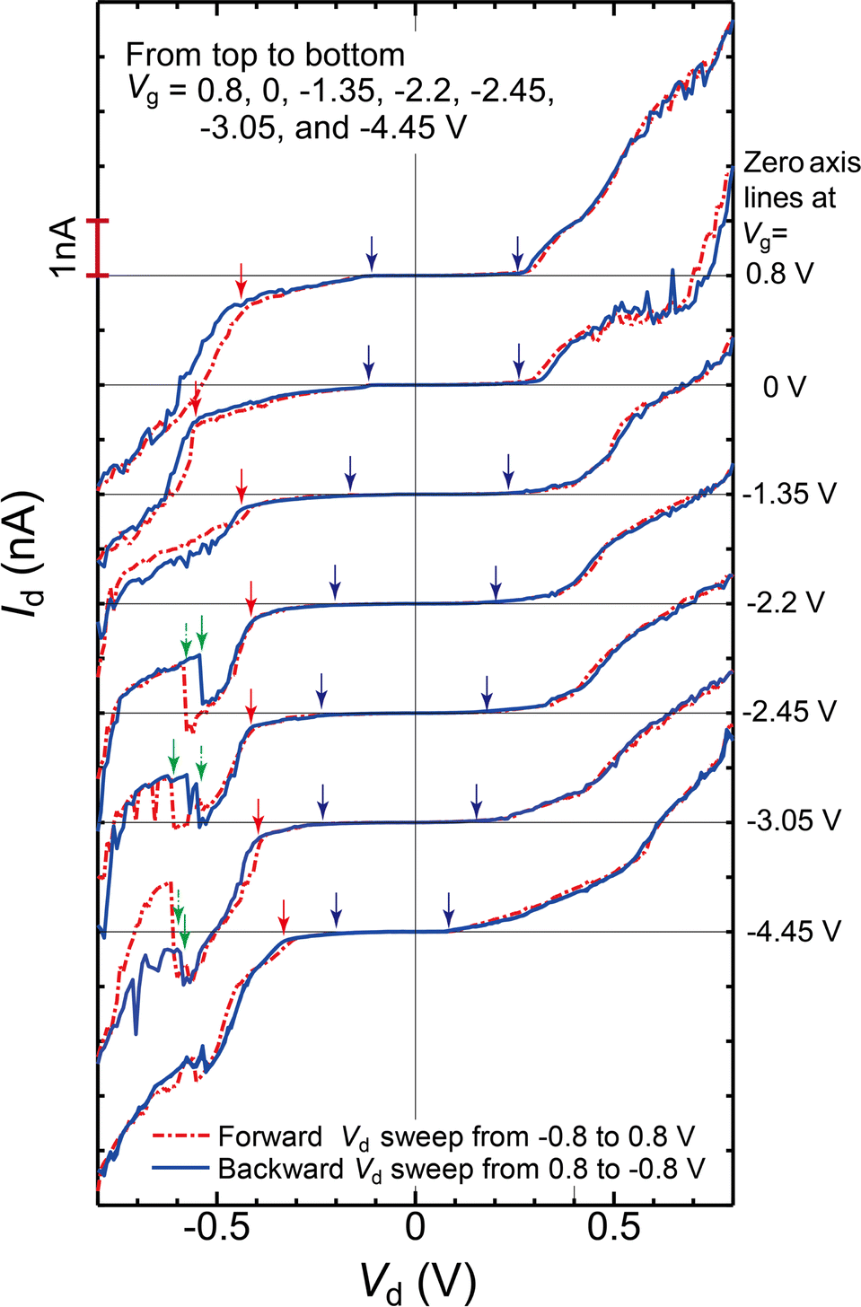 | ||
| Fig. 2 Experimental Id–Vd characteristics with Vg values of 0.8, 0, −1.35, −2.2, −2.45, −3.05, and −4.45 V under the consecutive forward (red dash-dotted lines) and backward (blue solid lines) Vd double sweeps between −0.8 and 0.8 V. Each Id–Vd curve is offset by 2 nA. No-current Vd regions are indicated by a pair of blue arrows. The steep current increases are indicated by red arrows. The abrupt current reductions are indicated by green solid (backward Vd sweep) and dash-dotted (forward Vd sweep) arrows and are observed at Vg values of −2.2, −2.45, and −3.05 V at Vd between −0.5 and −0.65 V. | ||
The no-current Vd region, indicated by a pair of blue arrows in Fig. 2, depended on Vg and increased with decreasing Vg from 0.8 to −2.2 V and then reduced with decreasing Vg from −2.2 to −4.45 V, suggesting Coulomb blockade phenomena. At positive Vd, steep increases of Id, indicated by red arrows, are observed at Vg between 0 and –4.45 V.
Then, abrupt current reductions, indicated by green arrows, are followed at Vd between −0.50 and −0.65 V. For example, Vd of the abrupt current reduction in the forward Vd sweep (green dash-dotted arrows: Vd = −0.58 and −0.62 V) differs from that in the backward Vd sweep (green arrows: Vd = −0.54 and −0.54 V) at Vg = −2.2 and −2.45 V, respectively. The Vd shifts at the abrupt current reduction between the forward and backward sweeps were 48 mV and 72 mV at Vg = −2.2 and −2.45 V, respectively. At Vd = −2.45 V, the spike current was also observed at Vd = −0.70 and −0.66 V in the forward Vd sweep and Vd = −0.57 V in the backward Vd sweep. Consequently, the abrupt current reduction should originate from the change in the trapped charge around the CdS QD, which shifted the discrete energy level of CdS QD under the Vd sweeps.
In contrast, in the Vd > −0.52 V and −0.63 < Vd < −0.73 V (except the spike current regions), the Id–Vd characteristics in the forward Vd sweep were equal to those in the backward Vd sweep, suggesting that the trapped charge states did not change and maintained at Vd > −0.52 V at Vg = −2.2 and −2.45 V, respectively.
Theoretical Coulomb staircase fitting was applied in the Vd region where the Coulomb blockade breaks and Id increases in the experimental Id–Vd curve at Vg = −2.2 V. The theoretical Coulomb staircase (Id–Vd) curve was calculated using the orthodox theory based on Fermi's golden-rule calculation on a double-barrier tunneling junction (DBTJ) system.30–34 Here, 5 parameters, as shown in the equivalent circuit in the inset of Fig. 3, the resistance and capacitance between the source and the Coulomb island (Rs, Cs), those between the Coulomb island and the drain (Rd, Cd), and offset charge of the Coulomb island Q0 are used. Fig. 3 shows theoretical and experimental Id–Vd curves at Vg = −2.2 V. The theoretical Id–Vd curve agrees with the experimental Id–Vd characteristics in three Vd regions from 0.3 to 0.4, from −0.3 to −0.4, and from −0.6 to −0.7 V. The values of the 5 parameters are evaluated to be Rs = 280 MΩ, Rd = 50 MΩ, Cs = 0.20 aF, Cd = 0.30 aF, and Q0 = 0.015 e (Vg = −2.2 V) (e: unit charge). The comparison of the theoretical Id–Vd curves when one of the 5 parameters is varied by ±5% is shown in Fig. S1(a)–(e) (ESI).† It notes that the value changes in ±5% give significantly different Id–Vd curves. As a result, the error ranges of each of the 5 parameters are within 10%.
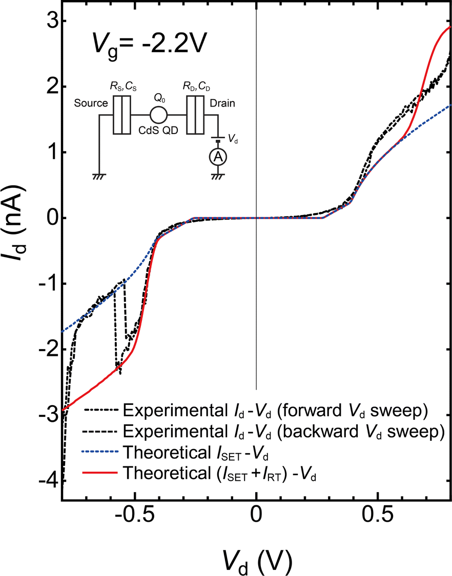 | ||
| Fig. 3 Theoretical Coulomb staircase (ISET–Vd) curve (blue dotted line), the sum of theoretical ISET and resonant tunneling current IRT (ISET + IRT)–Vd curve (red solid line), and experimental Id–Vd (forward (black dashed line) and backward (black dash-dotted line) Vd sweeps) curves at Vg = −2.2 V. The equivalent circuit of CdS-QD SET (inset). Five SET parameters are evaluated to be Rs = 280 MΩ, Rd = 50 MΩ, Cs = 0.20 aF, Cd = 0.30 aF, and Q0 = 0.015 e at 9 K (Vg = −2.2 V) (e: unit charge). Theoretical IRT is calculated based on the transmission probability on a single QD double barrier tunneling junction by using a standard deviation σ (17 meV) of the density of state (DOS) of the quantized energy level of CdS QDs and the center of DOS below the work function of the electrode μQD (0.275 eV). | ||
From these parameters, the charging energy, Ec (= e2/2 CΣ, CΣ = Cs + Cd), was estimated to be 163 meV. The experimental |Id| gradually increased at Vd between −0.3 and −0.4 V and apart from theoretical curves. Then, the abrupt current reduction followed −0.55 V. At Vd < −0.6 V, |Id| tends to increase again, and its value is much larger than the theoretical value.
Previously, we reported ideal single gold nanoparticle SET operations,35 and the capacitance of colloidal metallic nanoparticles as Coulomb islands was discussed based on a concentric sphere model.36,37 In contrast, the CdS QD is a dielectric material with a relative permittivity (ε1) of 5.7; the capacitance of the CdS QD (Cdot) can be calculated on a concentric dielectric sphere based on electromagnetism. Cdot is given by:
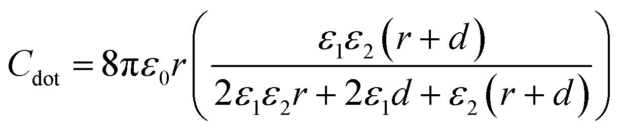 | (1) |
If we assume Cs and Cd of 0.20 and 0.30 aF as Cdot, the core diameter (2r) of the CdS QD is evaluated to be 2.9 and 4.6 nm from eqn (1), respectively. As the core of the CdS QD was chemisorbed through 1,16-hexadecanedithiol and placed near S/D electrodes, Cs and Cd should be slightly larger than Cdot. Consequently, the evaluated Cs and Cd values of 0.20 and 0.30 aF agree with an average CdS QD core diameter of 3.8 ± 0.4 nm (Fig. 1(b)). This agreement suggests that the CdS QD behaves as a Coulomb island in the SET, and the current rise regions in Id–Vd characteristics are attributed to Coulomb blockade phenomena on a single CdS QD.
The experimental Vd–Vg 2D dId/dVd plot is shown in Fig. 4. Herein, dId/dVd was calculated numerically from the experimental Id–Vd characteristics. As mentioned above, dId/dVd–Vd characteristics in the 2D plot also fluctuated owing to a slightly large Vd sweep range. Although the dId/dVd plot is noisy, Coulomb diamond is partially outlined as a pair of lines.39Vg dependence of the pair of inflection points at breaking Coulomb blockade was observed between −1.35 > Vg > −3.05 V in Fig. 4.
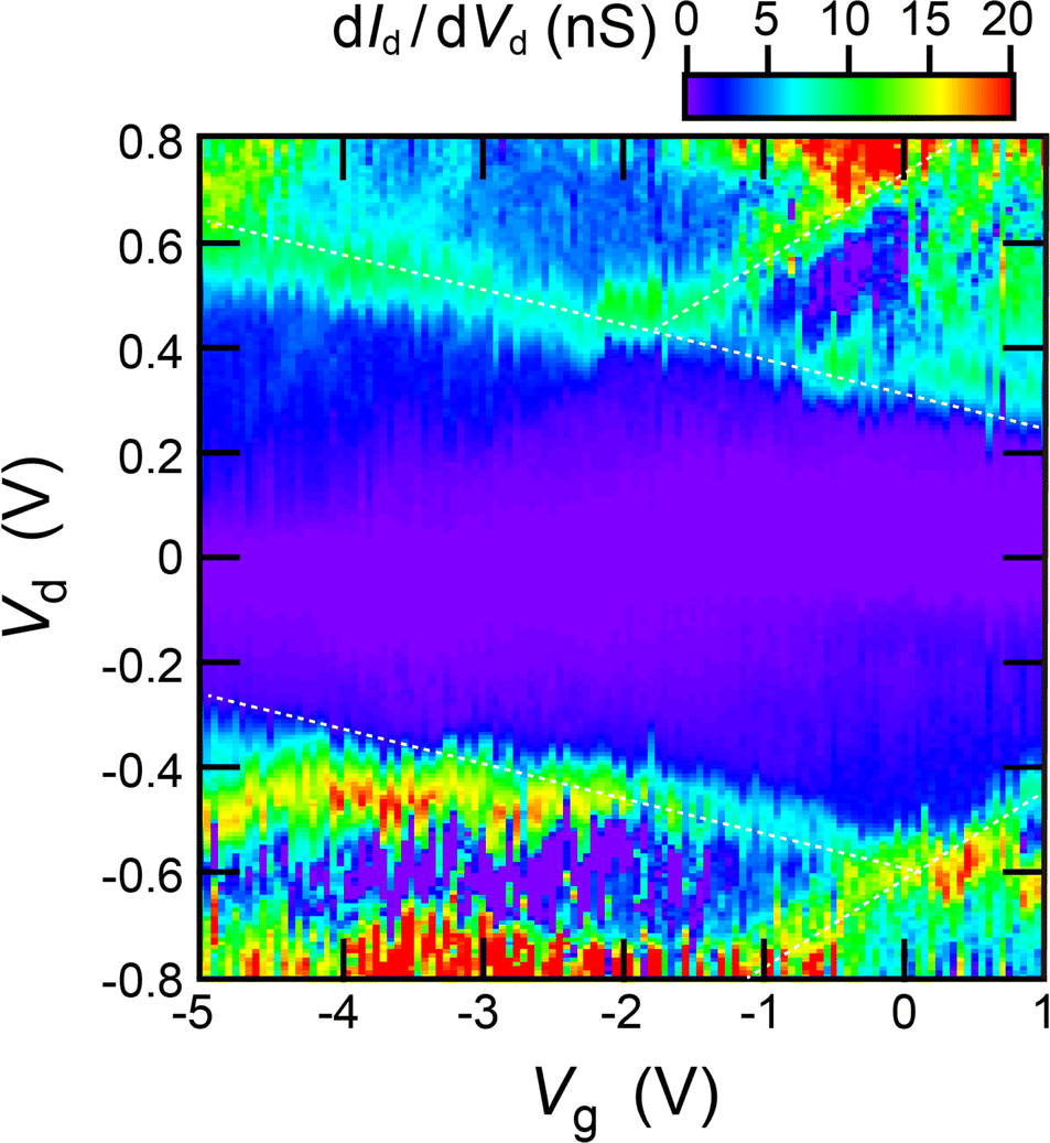 | ||
| Fig. 4 Experimental Vd–Vg 2D dId/dVd plot. The Coulomb diamond is outlined with white dotted lines. | ||
As shown in Fig. 3, the experimental initial current increases in the Vd region of −0.4 < Vd < 0.4 V, where the Coulomb blockade break agrees with the theoretical Id–Vd curve. In the negative Vd region of −0.55 < Vd < −0.4, the experimental Id–Vd curve was apart from the theoretical Coulomb staircase, and a steep increase in Id was observed as shown in Fig. 3. This steep increase in Id could be explained as the resonant tunneling through a discrete energy level of the CdS QD as follows.
Resonant tunneling current in a single QD double barrier tunneling junction is estimated from the transmission probability.40,41 Here, we assume that the transmission probability is proportional to the density of states (DOS) of the quantized energy level in the quantum dot (QD) within the voltage window between the source and drain electrodes. In addition, the density of states of the Au electrodes below and above the work function was assumed to be constant. The DOS of the quantized energy level in the QD is also considered a Gaussian distribution with a standard deviation σ.
In the double-barrier tunneling junction, Cs and Cd were estimated using the theoretical Coulomb staircase. When Vd is applied between the source and drain, the voltage shift (ΔVQD) of the DOS is expressed as
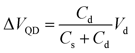 | (2) |
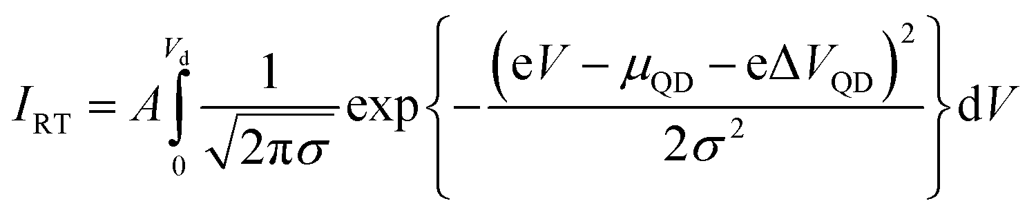 | (3) |
The theoretical IRT–Vd curve is shown in Fig. S2,† where μQD = 0.275 eV, σ = 17 meV, and A = 1.2 × 10⁻⁹ A. The sum of the theoretical (ISET + IRT) – Vd curve is shown in Fig. 3 (red solid line). It is noted that the theoretical (ISET + IRT) – Vd curve agrees with the experimental results where −0.5 V < Vd < −0.3 V. Consequently, the steep current increase in the Id–Vd characteristics originated from the resonant tunneling through a discrete energy level of the CdS QD.
The band diagrams of the CdS QD SET at the zero-bias voltage, the gradual current increase (ISET), the steep current increase (ISET + IRT), and the abrupt current reduction are shown in Fig. 5(a)–(d), respectively. The DOS of the quantized energy level of the CdS QD is expressed using a Gaussian distribution with a standard deviation σ, which exists below μQD from the work function of the source and drain electrodes, as shown in Fig. 5(a). When negative Vd is applied, DOS upshifts ΔVQD, the Coulomb blockade condition breaks, and ISET starts to flow, as shown in Fig. 5(b).
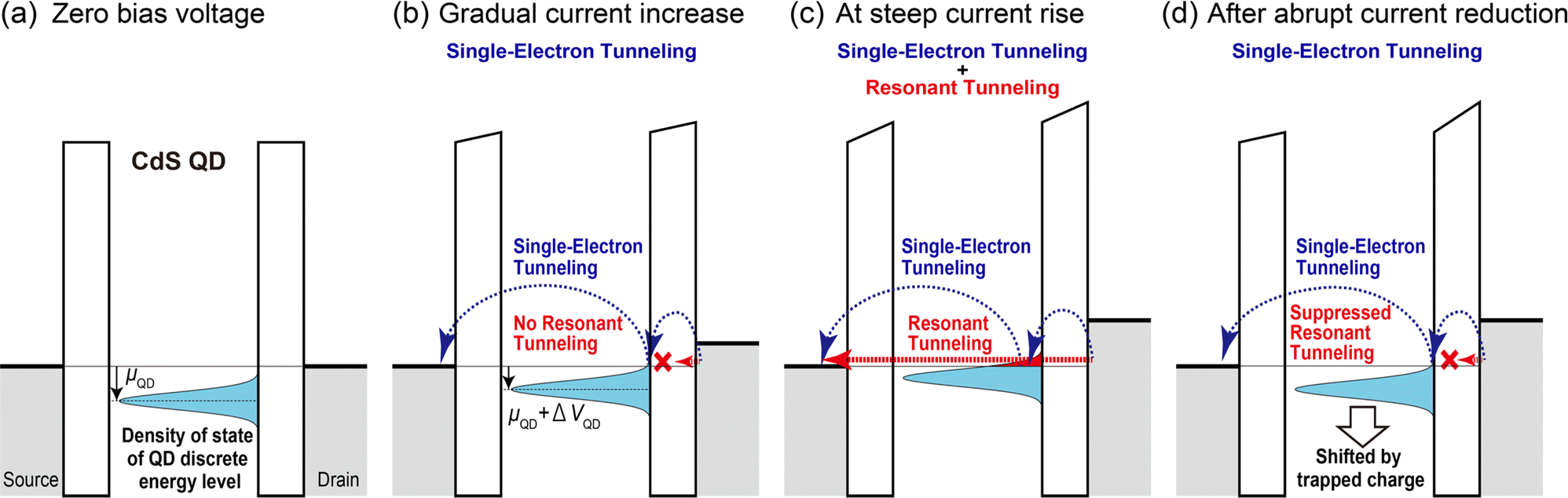 | ||
| Fig. 5 Band diagrams of a single CdS QD SET (a) at zero bias voltage, (b) gradual current increase, (c) steep current increase, and (d) after the abrupt current reduction by trapped charge around the CdS QD. The light blue and partially red Gaussian distribution represents the density of state at the CdS QD discrete energy level. Resonant tunneling and single-electron tunneling due to Coulomb blockade are shown as red dotted-line arrows and a pair of blue dotted-semicircle arrows, respectively. | ||
At the steep current rise region, as demonstrated in the theoretical (ISET + IRT)–Vd curve in Fig. 3, the resonant tunneling current IRT flowed at Vd < −0.4 as indicated by the red dotted line in Fig. 5(c), where the DOS of the discrete energy level of the CdS QD overlaps the voltage window between the source and drain electrodes (red region of DOS in Fig. 5(c)). As shown in the theoretical (ISET + IRT)–Vd curve in Fig. 3, IRT flowed at the steep current increase together with the single-electron tunneling current ISET (two blue dotted-semicircle arrows in Fig. 5(c)).
The change in the trapped charge should shift the discrete energy level of the CdS QD as shown in Fig. 5(d), and an abrupt current reduction was observed. Due to the trapped charge, the DOS of the discrete energy level shifted lower, and IRT was suppressed, as shown in Fig. 5(d). After the abrupt current reduction, Id became equal to the theoretical ISET–Vd curve, as shown in Fig. 3. Consequently, the abrupt current reduction on this CdS QD SET is attributed to the trapped charge around the CdS QD, which suppressed the resonant tunneling current.
The HS-Au/Pt nanogap-based CdS QD-SET is significant for the observation of the resonant tunneling current attributed to the existence of the discrete energy level and single-electron tunneling current based on Coulomb blockade phenomena.
Conclusions
In conclusion, resonant tunneling and single-electron tunneling effects based on the Coulomb blockade effect were observed in the Id–Vd characteristics and Vd–Vg 2D dId/dVd plot in a CdS (3.8 nm) QD-SET based on HS-Au/Pt nanogap electrodes with a gap separation of 4.5 nm. Experimental Id–Vd characteristics without the resonant tunneling effect agreed well with the theoretical curve based on the orthodox theory, which suggests that the electrical properties of this device originate from a CdS QD-SET. In the steep current rise region, the resonant tunneling current was observed and agreed well with the theoretical calculation based on the transmission probability at a single QD double barrier tunneling junction, where the single-electron tunneling current and the resonant tunneling current coexisted. The abrupt current reductions have been attributed to suppressing the resonant tunneling current caused by the trapped charge, which shifted the discrete energy level of the CdS QD. The HS-Au/Pt nanogap electrodes are a significant platform for observing electrical conduction in a single semiconductor QD, which opens a pathway to demonstrate their potential.Author contributions
Conceptualization: Y. M. and T. T.; methodology: Y. M. and G. O.; synthesis of CdS QDs: M. S. and T. T.; fabrication and measurement of the QD-SET: G. O. and T. N.; theoretical calculation: G. O. and Y. M.; analysis: G. O. and Y. M., writing – original draft: G. O.; writing – review and editing: Y. M.; funding acquisition: Y. M.Conflicts of interest
There are no conflicts to declare.Acknowledgements
This study was partially supported by JST CREST (JPMJCR22B4 and JPMJCR21B4), Japan, the MEXT Program: Data Creation and Utilization Type Material Research and Development (JPMXP1122683430), the International Collaborative Research Program of the Institute for Chemical Research, Kyoto University (grant # 2024-118), and Collaborative Research Projects (CRP), Laboratory for Materials and Structures, Institute of Innovative Research, Tokyo Institute of Technology. G.O. acknowledges the Support for Pioneering Research Initiated by the Next Generation (SPRING) program, JST (grant number JPMJSP2106). The authors thank Ms M. Miyakawa and Ms I. Shimada for their technical support.References
- A. I. Ekimov and A. A. Onushchenko, J. Exp. Theor. Phys. Lett., 1981, 34, 345–349 Search PubMed.
- M. A. Reed, J. N. Randall, R. J. Aggarwal, R. J. Matyi, T. M. Moore and A. E. Wetsel, Phys. Rev. Lett., 1988, 60, 535–537 CrossRef CAS PubMed.
- Y. Takahashi, H. Namatsu, K. Kurihara, K. Iwadate, M. Nagase and K. Murase, IEEE Trans. Electron Devices, 1996, 43, 1213–1217 CrossRef CAS.
- H. Ishikuro and T. Hiramoto, Appl. Phys. Lett., 1997, 71, 3691–3693 CrossRef CAS.
- L. Zhuang, L. Guo and S. Y. Chou, Appl. Phys. Lett., 1998, 72, 1205–1207 CrossRef CAS.
- M. Jung, K. Hirakawa, Y. Kawaguchi, S. Komiyama, S. Ishida and Y. Arakawa, Appl. Phys. Lett., 2005, 86, 033106 CrossRef.
- E. P. A. M. Bakkers, Z. Hens, A. Zunger, A. Franceschetti, L. P. Kouwenhoven, L. Gurevich and D. Vanmaekelbergh, Nano Lett., 2001, 1, 551–556 CrossRef CAS.
- M. R. Hummon, A. J. Stollenwerk, V. Narayanamurti, P. O. Anikeeva, M. J. Panzer, V. Wood and V. Bulović, Phys. Rev. B: Condens. Matter Mater. Phys., 2010, 81, 115439 CrossRef.
- K. Shibata, M. Yoshida, K. Hirakawa, T. Otsuka, S. Z. Bisri and Y. Iwasa, Nat. Commun., 2023, 14, 7486 CrossRef CAS PubMed.
- D. L. Klein, R. Roth, A. K. L. Lim, A. P. Alivisatos and P. L. McEuen, Nature, 1997, 389, 699–701 CAS.
- M. Zdrojek, M. J. Esplandiu, A. Barreiro and A. Bachtold, Phys. Rev. Lett., 2009, 102, 226804 CrossRef PubMed.
- M. Kobo, M. Yamamoto, H. Ishii and Y. Noguchi, J. Appl. Phys., 2016, 120, 164306 CrossRef.
- V. L. Colvin, M. C. Schlamp and A. P. Alivisatos, Nature, 1994, 370, 354–357 CAS.
- J. Lee, V. C. Sundar, J. R. Heine, M. G. Bawendi and K. F. Jensen, Adv. Mater., 2000, 12, 1102–1105 CrossRef CAS.
- S.-C. Lin, Y.-L. Lee, C.-H. Chang, Y.-J. Shen and Y.-M. Yang, Appl. Phys. Lett., 2007, 90, 143517 CrossRef.
- C. B. Murray, D. J. Norris and M. G. Bawendi, J. Am. Chem. Soc., 1993, 115, 8706–8715 CrossRef CAS.
- Y. Azuma, Y. Yasutake, K. Kono, M. Kanehara, T. Teranishi and Y. Majima, Jpn. J. Appl. Phys., 2010, 49, 090206 CrossRef.
- Y. Majima, G. Hackenberger, Y. Azuma, S. Kano, K. Matsuzaki, T. Susaki, M. Sakamoto and T. Teranishi, Sci. Technol. Adv. Mater., 2017, 18, 374–380 CrossRef CAS PubMed.
- C. Ouyang, K. Hashimoto, H. Tsuji, E. Nakamura and Y. Majima, ACS Omega, 2018, 3, 5125–5130 CrossRef CAS PubMed.
- Y. Y. Choi, T. Teranishi and Y. Majima, Appl. Phys. Express, 2019, 12, 025002 CrossRef.
- Y. Y. Choi, A. Kwon and Y. Majima, Appl. Phys. Express, 2019, 12, 125003 CrossRef CAS.
- M. Yang, R. Toyama, P. T. Tue and Y. Majima, Appl. Phys. Express, 2019, 13, 015006 CrossRef.
- S. J. Lee, J. Kim, T. Tsuda, R. Takano, R. Shintani, K. Nozaki and Y. Majima, Appl. Phys. Express, 2019, 12, 125007 CrossRef CAS.
- M. Saruyama, M. Kanehara and T. Teranishi, J. Am. Chem. Soc., 2010, 132, 3280–3282 CrossRef CAS.
- M. Singh, N. Kaur and E. Comini, J. Mater. Chem. C, 2020, 8, 3938–3955 RSC.
- M. Li, M. Liu, F. Qi, F. R. Lin and A. K.-Y. Jen, Chem. Rev., 2024, 124, 2138–2204 CrossRef CAS PubMed.
- J. Li, J. Chen, Y. Shen and X. Peng, Nano Res., 2018, 11, 3991–4004 CrossRef CAS.
- S. Baskoutas and A. F. Terzis, J. Appl. Phys., 2006, 99, 013708 CrossRef.
- A. Veamatahau, B. Jiang, T. Seifert, S. Makuta, K. Latham, M. Kanehara, T. Teranishi and Y. Tachibana, Phys. Chem. Chem. Phys., 2015, 17, 2850–2858 RSC.
- D. V. Averin and K. K. Likharev, J. Low Temp. Phys., 1986, 62, 345–373 CrossRef.
- C. W. J. Beenakker, Phys. Rev. B: Condens. Matter Mater. Phys., 1991, 44, 1646–1656 CrossRef PubMed.
- A. E. Hanna and M. Tinkham, Phys. Rev. B: Condens. Matter Mater. Phys., 1991, 44, 5919–5922 CrossRef PubMed.
- H. Zhang, Y. Yasutake, Y. Shichibu, T. Teranishi and Y. Majima, Phys. Rev. B: Condens. Matter Mater. Phys., 2005, 72, 205441 CrossRef CAS.
- Z. A. K. Durrani, Single-electron Devices and Circuits in Silicon, Imperial College Press, London, 2010 Search PubMed.
- S. Kano, D. Tanaka, M. Sakamoto, T. Teranishi and Y. Majima, Nanotechnology, 2015, 26, 045702 CrossRef CAS PubMed.
- S. Chen, R. W. Murray and S. W. Feldberg, J. Phys. Chem. B, 1998, 102, 9898–9907 CrossRef CAS.
- V. Garcia-Morales and S. Mafé, J. Phys. Chem. C, 2007, 111, 7242–7250 CrossRef CAS.
- M. D. Porter, T. B. Bright, D. L. Allara and C. E. D. Chidsey, J. Am. Chem. Soc., 1987, 109, 3559–3568 CrossRef CAS.
- Y. Ono and Y. Takahashi, Jpn. J. Appl. Phys., 2002, 41, 2569–2573 CrossRef CAS.
- R. Tsu and L. Esaki, Appl. Phys. Lett., 1973, 22, 562–564 CrossRef CAS.
- S. Datta, Electronic Transport in Mesoscopic Systems, Cambridge University Press, Cambridge, 1995 Search PubMed.
Footnote |
| † Electronic supplementary information (ESI) available. See DOI: https://doi.org/10.1039/d4na00288a |
| This journal is © The Royal Society of Chemistry 2024 |