
 Open Access Article
 This Open Access Article is licensed under a Creative Commons Attribution-Non Commercial 3.0 Unported Licence
On the structural evolution of nanoporous optically transparent CuO photocathodes upon calcination for photoelectrochemical applications†
Lukas
Korell
a,
Stefan
Lauterbach
b,
Jana
Timm
c,
Li
Wang
d,
Maximilian
Mellin
 a,
Anna
Kundmann
d,
Qingyang
Wu
a,
Chuanmu
Tian
a,
Roland
Marschall
c,
Jan P.
Hofmann
a,
Frank E.
Osterloh
d and
Marcus
Einert
*a
a,
Anna
Kundmann
d,
Qingyang
Wu
a,
Chuanmu
Tian
a,
Roland
Marschall
c,
Jan P.
Hofmann
a,
Frank E.
Osterloh
d and
Marcus
Einert
*a
aSurface Science Laboratory, Department of Materials and Earth Sciences, Technical University of Darmstadt, Otto-Berndt-Straße 3, 64287 Darmstadt, Germany. E-mail: meinert@surface.tu-darmstadt.de
bInstitute for Applied Geosciences, Geomaterial Science, Technical University of Darmstadt, Schnittspahnstraße 9, 64287 Darmstadt, Germany
cDepartment of Chemistry, University of Bayreuth, Universitätsstraße 30, 95447 Bayreuth, Germany
dDepartment of Chemistry, University of California, One Shields Avenue, Davis, CA 95616, USA
First published on 19th April 2024
Abstract
Copper oxides are promising photocathode materials for solar hydrogen production due to their narrow optical band gap energy allowing broad visible light absorption. However, they suffer from severe photocorrosion upon illumination, mainly due to copper reduction. Nanostructuring has been proven to enhance the photoresponse of CuO photocathodes; however, there is a lack of precise structural control on the nanoscale upon sol–gel synthesis and calcination for achieving optically transparent CuO thin film photoabsorbers. In this study, nanoporous and nanocrystalline CuO networks were prepared by a soft-templating and dip-coating method utilizing poly(ethylene oxide)-block-poly(propylene oxide)-block-poly(ethylene oxide) (Pluronic® F-127) as a structure-directing agent, resulting for the first-time in uniformly structured, crack-free, and optically transparent CuO thin films. The photoelectrochemical properties of the nanoporous CuO frameworks were investigated as a function of the calcination temperature and film thickness, revealing important information about the photocurrent, photostability, and photovoltage. Based on surface photovoltage spectroscopy (SPV), the films are p-type and generate up to 60 mV photovoltage at 2.0 eV (0.050 mW cm−2) irradiation for the film annealed at 750 °C. For these high annealing temperatures, the nanocrystalline domains in the thin film structure are more developed, resulting in improved electronic quality. In aqueous electrolytes with or without methyl viologen (as a fast electron acceptor), CuO films show cathodic photocurrents of up to −2.4 mA cm−2 at 0.32 V vs. RHE (air mass (AM) 1.5). However, the photocurrents were found to be entirely due to photocorrosion of the films and decay to near zero over the course of 20 min under AM 1.5 illumination. These fundamental results on the structural and morphological development upon calcination provide a direction and show the necessity for further (surface) treatment of sol–gel derived CuO photocathodes for photoelectrochemical applications. The study demonstrates how to control the size of nanopores starting from mesopore formation at 400 °C to the evolution of macroporous frameworks at 750 °C.
Introduction
Since global energy consumption is rising, scientists all over the world are searching for new, more sustainable possibilities of energy conversion and storage. For storage of renewable energy, it is from a logistics point of view beneficial to choose a chemical fuel, such as hydrogen, rather than batteries or mechanical storage systems owing to the already existing storage and transport infrastructure.1–3 Photoelectrochemical (PEC) water splitting on semiconducting photoelectrodes allows direct conversion of solar energy into hydrogen with a single integrated device.4,5 PEC water splitting research was pioneered by Fujishima and Honda in 1972,6 after discovery of photoelectrochemical water oxidation with TiO2 by Boddy in 1968.7 Since then, more efficient and stable photoelectrode materials have been developed in many studies.4,5,8–11 Especially, earth-abundant metal oxides are well studied photoabsorber materials for PEC water splitting12,13 due to their natural abundance, good processability, and improved stability in oxidative environments (without the necessity of protection layers), especially when compared to sulfides and nitrides – all factors leading to substantially lower production costs.12,14 However, binary metal oxides including α-Fe2O3,15,16 WO3,17,18 TiO2,19,20 and ZnO21 and ternary metal oxides, such as BiVO4![[thin space (1/6-em)]](https://www.rsc.org/images/entities/char_2009.gif) 22,23 and CuBi2O424,25 are still not meeting the required demands for commercialization due to insufficient energy conversion efficiencies. This is partly a result of photovoltage losses resulting from polaron formation effects in metal oxides.26 To increase the photovoltage, a tandem cell approach is a promising strategy since the photovoltages of the two photoabsorbers are added.2,27 However, there is a lack of available low-band-gap metal oxide photoabsorbers, especially with respect to p-type semiconductors. Hence, it is important to study and optimize the photoelectrochemical properties of photocathodes possessing a low band gap energy. In this context, the hole conductor cupric oxide (CuO, p-type) is a promising nontoxic photocathode material with a direct optical band gap energy between 1.3 eV and 1.6 eV.28–30 The optical energy transition in CuO allows strong absorption from the visible spectrum of light, thus being theoretically capable of achieving maximum solar-to-hydrogen efficiencies above 30%.29,31 The conduction band minimum (CBM) of CuO is located between −0.8 and −1.0 V vs. RHE,32,33 which is suitable for water reduction (0.0 V vs. RHE). However, this is also the main drawback of CuO applied as a photocathode, as it suffers from severe photocorrosion, since the photoexcited charge carriers also reduce Cu2+ to Cu+ (0.15 V vs. RHE).29,30 As a consequence, the formation of CuO/Cu2O heterojunctions is well documented in the literature, leading to a substantial stabilization effect of the electrode–electrolyte interface owing to improved spatial charge carrier separation between the two phases.34–36 In contrast to the frequently utilized cuprous oxide (Cu2O), CuO demonstrates a better photoelectrochemical performance owing to the 2–3 fold higher electric conductivity,37,38 enhanced light absorption over the entire solar spectrum,29,38,39 and higher photostability when prepared via sol–gel routes.38
22,23 and CuBi2O424,25 are still not meeting the required demands for commercialization due to insufficient energy conversion efficiencies. This is partly a result of photovoltage losses resulting from polaron formation effects in metal oxides.26 To increase the photovoltage, a tandem cell approach is a promising strategy since the photovoltages of the two photoabsorbers are added.2,27 However, there is a lack of available low-band-gap metal oxide photoabsorbers, especially with respect to p-type semiconductors. Hence, it is important to study and optimize the photoelectrochemical properties of photocathodes possessing a low band gap energy. In this context, the hole conductor cupric oxide (CuO, p-type) is a promising nontoxic photocathode material with a direct optical band gap energy between 1.3 eV and 1.6 eV.28–30 The optical energy transition in CuO allows strong absorption from the visible spectrum of light, thus being theoretically capable of achieving maximum solar-to-hydrogen efficiencies above 30%.29,31 The conduction band minimum (CBM) of CuO is located between −0.8 and −1.0 V vs. RHE,32,33 which is suitable for water reduction (0.0 V vs. RHE). However, this is also the main drawback of CuO applied as a photocathode, as it suffers from severe photocorrosion, since the photoexcited charge carriers also reduce Cu2+ to Cu+ (0.15 V vs. RHE).29,30 As a consequence, the formation of CuO/Cu2O heterojunctions is well documented in the literature, leading to a substantial stabilization effect of the electrode–electrolyte interface owing to improved spatial charge carrier separation between the two phases.34–36 In contrast to the frequently utilized cuprous oxide (Cu2O), CuO demonstrates a better photoelectrochemical performance owing to the 2–3 fold higher electric conductivity,37,38 enhanced light absorption over the entire solar spectrum,29,38,39 and higher photostability when prepared via sol–gel routes.38
Nanostructuring and photostability of CuO
Morphology control – such as nanostructuring – in metal oxides applied as photoelectrodes is a general synthetic concept to decrease the charge carrier migration paths, and thus to inhibit recombination, especially in the bulk structure.8,40 Nanostructuring of metal oxides possessing low minority charge carrier diffusion lengths is therefore one of the most effective strategies to improve the overall photoresponse and -stability of photoelectrode systems. For example, hematite, one of the most studied photoabsorbers, with its poor electronic charge carrier transport properties, has been proven to benefit from the creation of nanoscale transport distances for migrating charge carriers.40,41 Regarding nanostructuring of CuO photoabsorbers, decreasing the size of structural features, such as the crystallite size, and forming porous structures was claimed to improve the photoelectrochemical performance due to increased surface areas and, consequently, more reaction sites for the solar-driven hydrogen evolution reaction.42–44 Even though nanostructuring seems to help suppress photocorrosion, about 55% of the photocurrent still has been assigned to reduction of copper ions to metallic copper,45 emphasizing the demand for a detailed analysis and optimization of the CuO (nano-) morphology and electronic structure. In this context, the Bein group has intensively investigated the photostability of CuO photocathodes, achieving a faradaic hydrogen production efficiency of 91% over 15 minutes through improvement of the PEC properties by Li doping and deposition of a 2.5 nm Ti0.8Nb0.2Ox protection layer.30 In this study, they observed that Li-doped CuO forms Cu2O under illumination at 0.2 V vs. RHE (in 1 M Na2SO4, pH 7), but is also photostable at higher voltages, as confirmed via XPS. They also proved the evolution of hydrogen in response to illumination of their electrode by using a hydrogen sensor. The reported faradaic efficiency of 61% after 10 minutes showed that a higher proportion of current is coming from hydrogen evolution compared to photocorrosion.In principle, distinct CuO morphologies have been prepared in the form of nanoparticles,46 nanorods,47,48 nanosheets,49 nanowires,50 and nanofibers.51 Especially, CuO nanofibers fabricated by electrospinning have been reported to show exceptional photostability under operating conditions in an aqueous sodium sulfate electrolyte, albeit with low photocurrents in the µA-range. The CuO nanofibers retain over 50% of their initial photoresponse after the fifth PEC measurement and reveal no further current loss over hours.51
In the arsenal of morphology control at the nanoscale, the concept of meso-/nanostructuring of thin films by soft-templating via the evaporation-induced self-assembly (EISA) process is an easy-to-handle, low-cost, and scalable approach.52 Based on the appropriate selection of the structure-directing agent,53 which typically includes the utilization of amphiphilic block-copolymers, the pore geometry, pore order, pore diameter, and connectivity of the mesoporous network can be controlled precisely, thus allowing tailored design of the nanoarchitecture. The fine tuning of the nanoporous framework is of importance with respect to the mass transport,54 significantly influencing the PEC properties, especially in metal oxides.55
The Laberty-Robert group synthesized CuO thin films by a sol–gel-based dip-coating approach and presented that the photoresponse depends on the crystallinity and microstructure.43 The best-performing dense CuO thin film (−0.94 mA cm−2 at 0 V vs. RHE) was found for a calcination temperature of 400 °C and 500 nm thickness. Interestingly, the usage of poly-iso-butylene-b-polyethylene oxide (PIB-b-PEO), which typically leads to the fabrication of ordered mesoporous metal oxide networks when applied as a structure-directing agent,56,57 was reported to result in poor organization. This was attributed to the degradation of PIB-b-PEO at 200 °C before the crystallization of CuO could occur, expected at 300 °C.43 However, in the work of Marschall et al.,58 the lowest reported temperature for the thermal decomposition of PIB-b-PEO to begin was 310 °C (with the main degradation derivative at 385 °C), a difference which might be attributed to the deviating molecular weights of the polymers. Uchiyama et al. synthesized nanoporous CuO photocathodes by utilization of polyvinyl pyrrolidone (PVP) upon dip-coating.42 The authors assigned the enhanced photoelectrochemical performance to the large surface area, originating from the highly porous CuO structure. The results indicate the necessity of finding an appropriate organic template for which thermal degradation coincides with crystallization of CuO in order to produce nanoporous CuO thin films with a well-defined and homogenous through-pore structure within the entire thin film, allowing thorough permeation of the electrolyte.
Kyesmen et al. investigated the impact of the film thickness of CuO nanostructures synthesized by (multiple) dip-coating steps on their PEC water splitting performance.59 The ideal film thickness was found to be 419 ± 37 nm, corresponding to six-times dip-coated CuO films calcined at 550 °C. The highest photocurrent density of −2 mA cm−2 at 0.45 V vs. RHE was ascribed to the optimum light absorption and the porous nature of the film's surface, which led to a larger surface area, and thus, increased number of active sites for the water reduction reaction.59 Related to these findings, a systematic study on the surface area and pore order of mesoporous CuFe2O4 photoanodes postulated a general trend that the photoinduced water and sulfite oxidation reactions are predominantly determined by the surface area of the photoabsorber.55 In particular, the sulfite oxidation, which is a thermodynamically down–hill reaction (ΔG < 0),60 is accelerated at high-surface-area materials since sulfite is a fast hole acceptor.61 Therefore, the sulfite oxidation is dominated by the number and availability of reactive surface sites.55 Based on these data, the investigation of the PEC properties of metal oxide-based nanoporous photoelectrodes toward sulfite oxidation is advantageous compared to compact/dense film structures (with low surface areas) since they offer plenty of reaction centers and allow for thorough penetration of the electrolyte (improved mass transport).
In this work, the commercially available, inexpensive tri-block-copolymer Pluronic® F-127 was utilized for the first time for the preparation of nanoporous and nanocrystalline CuO thin films by dip-coating and soft-templating. In order to study the fundamental impact of nanostructuring on the physicochemical and PEC properties (structure–property–function relationship), the CuO samples were thermally treated at variable temperatures and synthesized with variable film thicknesses. While the nanoporous CuO framework develops larger pores and particles with increasing temperature, thus improving the electronic transport properties, the temperature-dependent increase of the photoresponse was found to be predominantly ascribed to photocorrosion effects.
Results and discussion
Structural characterization
In order to synthesize well-defined and reproducible nanoporous (defined as pores between 1 nm and 100 nm, whereas mesopores and macropores are 2–50 nm and >50 nm in diameter, respectively) CuO thin films, the intrinsic (e.g., precursor and solvent concentration) as well as the extrinsic (e.g., humidity) experimental parameters needed to be precisely optimized for the dip-coating process (Fig. S1†). It was found that homogenous and crack-free samples – on the meso- and macroscale (see Fig. 1) – were only attained by choosing a low relative humidity (RH) of 18% and utilizing 2-methoxyethanol as main-solvent for selectively dissolving the metal precursor (copper nitrate) and the porogen (Pluronic® F-127), followed by adding the co-solvent ethanol.62 Mixing of both organic solutions allows for precise adjustment of their evaporation rate and thus to control the drying process of the as-deposited, amorphous thin film layers, predetermining the formation of a structurally intact and (inter-) connected nanoporous architecture. The direct transfer of the freshly dip-coated samples into a pre-heated furnace (125 °C) was critical to the stabilization of the CuO framework, due to desorption of hydroxyl and water molecules from the samples' surfaces followed by a 24 h stabilization step at 250 °C for 24 hours to allow for sufficient condensation of the hydrolyzed precursors.58,63,64 Even though fabrication of porous CuO thin films by dip-coating has been studied,65–69 preparation of uniform and continuously connected nanoporous and optically transparent CuO thin films by soft-templating (using a copolymer as structure-directing agent) via the EISA method has, to the best of our knowledge, not been reported yet. Advantageously, the EISA process allows for precise control for adjusting the porosity,52,70 and thus the mass transport properties,71 when the nanoporous network is in contact with an electrolyte.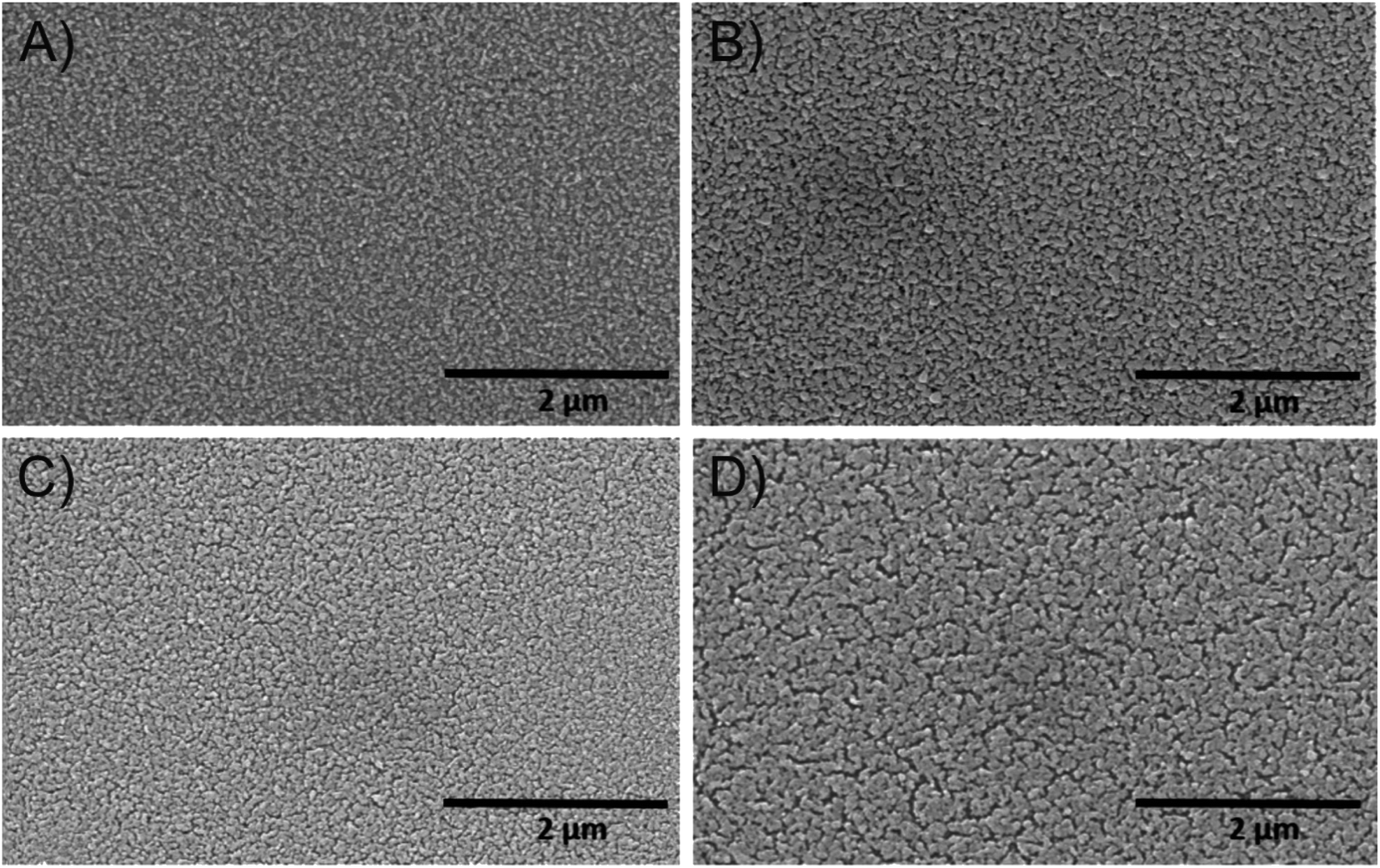 | ||
| Fig. 1 Large-scale SEM images of the mesoporous (A) CuO-400, (B) CuO-500, (C) CuO-600, and (D) CuO-750 thin film photocathodes. | ||
In order to investigate the impact of calcination temperature and structural evolution on the PEC activity, the CuO thin films were calcined at 400 °C, 500 °C, 600 °C, and 750 °C, in the following referred to as CuO-400, CuO-500, CuO-600, and CuO-750, respectively. Scanning electron microscopy (SEM) was used to investigate the surface morphology of the CuO films and to determine the (secondary) particle sizes of the nanoporous CuO network. After careful optimization of the synthesis parameters, the thin films were composed of interconnected nanostructures/-grains forming a disordered porous framework with the absence of any macroscopic cracks (Fig. 1 and 2). Additionally, all structures were found to be crack-free on the nanoscale independent of the calcination temperature, proving that a homogenous and uniform architecture was constructed. The elucidation of the particle size from the SEM images demonstrates that the nanoparticles grow with increasing calcination temperature. This increase of the crystal size is attributed to the thermal annealing, which was also reported in sol–gel-derived nanofibrous CuO thin films.51 Typically, nanostructures provide short diffusion paths and are not in a thermodynamic equilibrium;72 therefore, dissolution of atoms and transfer to grain boundaries occur with increasing temperatures, resulting in the growth of nanoparticles. The appearance of the CuO particles calcined at low temperatures (400 °C) show rounder shapes which might be interpreted as partially amorphous structures, while the particles/crystals in the films annealed at higher temperatures (>500 °C) show more clear edges. For CuO-400, CuO-500, CuO-600, and CuO-750 (secondary) particle sizes range between 21–49 nm, 24–66 nm, 28–69 nm, and 30–72 nm, respectively.
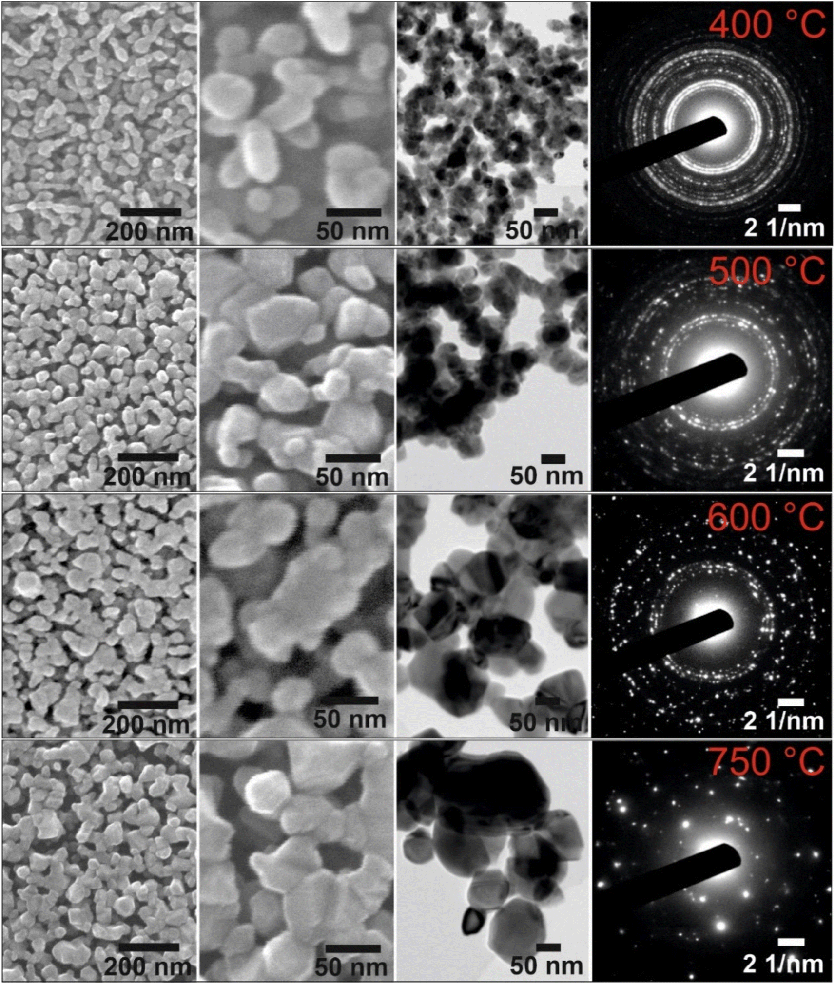 | ||
| Fig. 2 Scanning and transmission electron microscopy images of mesoporous and nanocrystalline CuO-400 (top row), CuO-500 (2nd row), CuO-600 (3rd row), and CuO-750 thin films (4th row) at low (SEM) and high (TEM) magnifications. The corresponding selected-area electron diffraction patterns are shown in the right-hand column demonstrating the coarsening of the CuO crystallites with increasing annealing temperature. | ||
Transmission electron microscopy (TEM) was used to evaluate the crystal morphology and to verify the meso- and macroporosity of the CuO samples. The bright spots visible in the TEM images (Fig. 2 and S2†) clearly prove that the CuO thin films indeed consist of nanoporous features present throughout the entire bulk structure (also shown in bright-field TEM images in Fig. S3†). TEM-based energy dispersive X-ray spectroscopy (EDXS, Fig. S3†) proved the presence of copper, oxygen, and carbon in all CuO thin films, the latter element originating from residual Pluronic® F-127 and adsorbed hydrocarbons (see XPS Fig. S5†). The TEM data are consistent with the observed morphology and particle sizes determined by SEM. Selected area electron diffraction (SAED) patterns can be indexed to the monoclinic crystal structure of CuO, which is exemplarily presented for the CuO-400 sample (Fig. S2A†). In addition, the SAED patterns demonstrate the coarsening of the CuO crystallites with increasing annealing temperature (in accordance with the SEM and GIWAXD data). The convergent electron beam diffraction (CEBD) pattern of the CuO-750 sample (Fig. 3A) shows diffraction on a single nanocrystal and the observed reflections also match to the monoclinic CuO phase. In general, the film thickness influences the optical absorbance (penetration depth of light) and consequently the photoelectrochemical properties of a photoelectrode. Hence, the film thickness of the four control samples was analyzed by profilometry (Fig. S4†), indicating thicknesses of 230 nm (±20 nm), 250 nm (±20 nm), 230 nm (±20 nm), and 300 nm (±20 nm) for the CuO-400, CuO-500, CuO-600, and CuO-750, respectively. The nanoporous CuO thin films calcined between 400 °C and 600 °C possess the same thicknesses, considering an average error of 20 nm. The determined film thicknesses are in a typical range observed for chemically different but structurally related sol–gel derived transition metal oxide thin films also prepared by the dip-coating and EISA process.73 However, the CuO-750 sample was evaluated to be substantially thicker, most likely due to the difference in surface topography and morphology of the ITO compared to the FTO substrate, resulting in distinct adhesion and wettability properties of the dip-coating solution. In order to correlate the observed particle sizes in a quantitative manner to the specific surface area of the films (allowing for a precise interpretation), Krypton physisorption measurements were carried out at 77 K. The specific surface areas of the CuO-400, CuO-500, CuO-600, and CuO-750 were evaluated to be 5.0 m2 g−1, 15.4 m2 g−1, 15.1 m2 g−1, and 3.8 m2 g−1. This trend is in accordance with the evaluated crystallite sizes by XRD considering the fact that the organic template Pluronic® F-127 is not fully decomposed at 400 °C.63 In the CuO-400 sample, hydrocarbons (detected by XPS, Fig. S5†) originating from the residual polymer, most likely block available adsorption sites for the krypton atoms within the nanoporous network, resulting in relatively low specific surface areas (5.0 m2 g−1). However, after annealing at 500 °C, the polymer is completely degraded (thermogravimetric analysis show 98% weight loss of Pluronic® F-127 after 462 °C in air)63 and – at the same time – the nanoporous network is fully developed (through-pore structure), which is represented by the largest surface area (15.4 m2 g−1) among all samples. With increasing annealing temperature, the CuO nanocrystals steadily grow (see Fig. 1 and 2) leading to extension of the meso- and macropores (higher macro-/mesopore ratio), and thus, to lower total surface areas. In accordance with literature, the CuO-750 thin films exhibit the lowest surface area (3.8 m2 g−1), which was likewise found for the surface area-temperature dependency of CuO-nanofibers.51
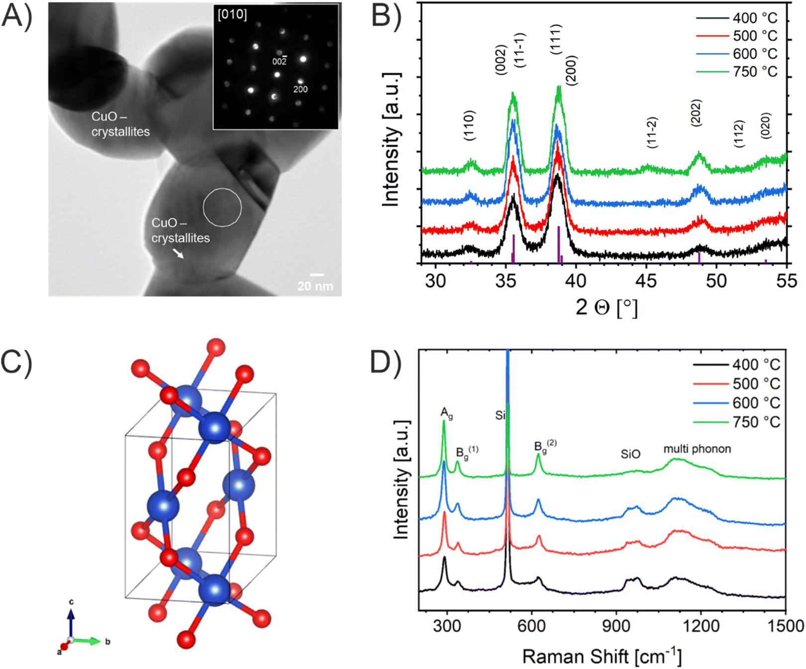 | ||
| Fig. 3 (A) Bright-field TEM image of CuO-750 with the inset presenting a convergent electron beam diffraction (CEBD) pattern recorded in the marked area (circle). The pattern is indexed according to the monoclinic CuO phase. (B) X-ray diffraction patterns of mesoporous CuO-400, CuO-500, CuO-600, and CuO-750 thin films shown with reference bars corresponding to JCPDS no. 01-089-5899. (C) Crystal structure of monoclinic CuO; red: Cu atoms, blue: O atoms. (D) Raman spectra of mesoporous CuO-400, CuO-500, CuO-600, and CuO-750 thin films (λex = 514 nm). | ||
For the evaluation of the crystallographic structure and crystallite size depending on the calcination temperature, all samples were analyzed by grazing-incidence wide-angle X-ray diffraction (GIWAXD). Fig. 3B exhibits the diffraction patterns of the mesoporous CuO-400, CuO-500, CuO-600, and CuO-750 thin films, illustrating pronounced Bragg peaks at 2θ = 32.3°, 35.3°, 38.5°, and 48.7° which could be consistently indexed to the (110), (11−1), (111) and (20−2) lattice planes of the monoclinic phase according to JCPDS no. 01-089-5899 (reference bars shown as violet bars in Fig. 3B). All samples solely crystallize in the monoclinic CuO phase with space group C2/c symmetry independent of the annealing temperature and no further secondary phases and/or impurities were detected. The increase in intensity at 2θ = 55° is related to the reflections of the silicon substrate.55 Since the monoclinic crystal structure (shown in Fig. 3C) is the thermodynamically most stable form of CuO, this phase was also detected for other sol–gel derived and thermally treated CuO samples.38,43,51 Interestingly, the intensity of the diffraction peaks related to the background noise increases for higher calcined samples owing to the development of more crystalline nanodomains (allowing stronger diffraction of the X-rays). As a consequence, the diffraction peaks were found to be more pronounced, which can be exemplarily observed for the (11−2) reflection of the CuO-750 sample. By applying the Williamson–Hall method,74,75 the crystallite/primary particle size was determined from the well-separated (110), (202), and (004) peaks. The crystallite size increases from 9 nm calculated for CuO-400 to 14 nm for CuO-750 thin films (note that the crystallite size does not represent the agglomerated secondary particle sizes visualized in the SEM images). The data prove the thermally induced growth of nanocrystals within the porous architecture. The full-width at half-maximum (FWHM) values and the determined crystallite sizes for the (110)-reflection are shown and compared in Table S1.† To verify the crystallographic structure determined by GIWAXD/CEBD and to exclude any secondary phase formation, Raman spectroscopy was conducted since it is a more sensitive technique toward the detection of (phase) impurities. The Raman spectra of the CuO-400, CuO-500, CuO-600, and CuO-750 thin films are shown in Fig. 3D. The spectra of all samples have three Raman active phonon modes at 292 cm−1, 338 cm−1, and 615 cm−1, which can be assigned to the Ag, Bg(1) and Bg(2) bands – the three typical one-dimensional optical phonon modes observed for monoclinic (nanocrystalline) CuO.76–78 In addition, there are two peaks located at 496 cm−1 and between 910 cm−1 and 980 cm−1 originating from the silicon substrate and which are related to silicon (Si) and to silicon oxide (SiO), respectively. Besides the described Raman bands, no additional peaks could be found in the spectra, indicating the phase-purity of all CuO samples, regardless of treatment temperature. Interestingly, peak broadening appears for lower calcination temperatures, which is a reasonable observation since the crystallite size for the CuO-400 was 9 nm compared to the 14 nm for the CuO-750, which fits the description of a nanoconfined space.77,79 This phenomenon can be generally ascribed to the nanoconfinement effect, which is based on the Heisenberg uncertainty principle. It states that as the particle size decreases and the system becomes spatially more localized, the energy distribution must become more delocalized (here in the form of peak broadening) in order to satisfy the uncertainty principle  .20 Furthermore, the Ag peak reveals a slight red shift from 292 cm−1 to 287 cm−1 as the calcination temperature increases from 400 °C to 750 °C. This red shift of the Ag peak for nanocrystalline CuO thin films, which is typically located at 298 cm−1,76 can be attributed to the impact of temperature as it was reported by Ravi et al.78 In that study, it was demonstrated that a laser heat up of CuO samples results in a red shift of the Raman peaks.77,78 The broad bands between 1000 cm−1 and 1300 cm−1 can be attributed to multi-phonon scattering effects of CuO.77 To study the chemical composition and the Cu oxidation state of the CuO samples, X-ray photoelectron spectroscopy (XPS) was conducted. The survey spectra of CuO-400, CuO-500, and CuO-600 are shown in Fig. S5.† Besides the photoemission peaks, which were related to the Cu 2p and O 1s orbitals, a less-pronounced C 1s peak was identified for all three samples. The C 1s signal was attributed to surface adsorbed hydrocarbon species typically detected on sol–gel derived metal oxide thin films.23,73 The absence of any other elements in the survey spectrum supports the GIWAXD and Raman data stating phase-purity of all investigated CuO samples, independent of the calcination temperature. Fig. 4A depicts the high-resolution XPS scans of the Cu 2p spectra including the spin–orbit splitting with the corresponding peak positions of the Cu 2p1/2 and Cu 2p3/2 orbitals at binding energies of 954.3 eV and 933.3 eV, respectively, which were elucidated for the CuO-400, CuO-500, CuO-600, and CuO-700 thin films. Both peak positions are consistent with the literature values reported for nanostructured sol–gel derived CuO.38,51 Both the Cu 2p1/2 and Cu 2p3/2 peaks possess satellite features at binding energies of 960–965 eV and 940–946 eV, respectively, with a distinct shoulder for lower binding energies, indicative of Cu being present at the surface in the oxidation state +2.80 The O 1s spectra of the investigated CuO samples (Fig. 4B) show the main emission lines at 530.2 eV and a pronounced shoulder with a main intensity at 531.9 eV. The main peak originates from lattice oxygen. The appearance of a pronounced shoulder located between 531 eV and 534 eV can be assigned to hydroxyl groups and adsorbed water molecules on the surface of the samples and was found to be highest for CuO-750.81 Interestingly, for CuO-400, CuO-500, and CuO-600 no trend over the annealing temperature for the ratio of the main O 1s peak and the shoulder was observed, suggesting that the amount of defective oxygen (including oxygen vacancies) and/or hydroxyl groups is not changing for applied temperature profiles between 400 °C and 600 °C. However, for calcination temperatures of 750 °C the concentration of adsorbed water and hydroxyl groups drastically increases, most likely owing to larger nanopores allowing for better adsorption. From a surface compositional point of view, an impact of adsorbed species and/or oxygen vacancies on the photoelectrochemical performances, as reported for CuO82 and BiOCl,83 cannot be excluded, which might partially explain the delayed and reduced photocorrosion observed for CuO-750 (see Fig. 6C). In conclusion, the calcination temperature did not significantly affect the relative binding energy positions of the Cu 2p and O 1s photoemission lines (except for CuO-750 a slightly higher binding energy is observed owing to hydroxyl species and adsorbed water molecules), allowing the assumption that the oxidation states and chemical speciation of Cu and O at the surface are comparable among all calcination temperatures.
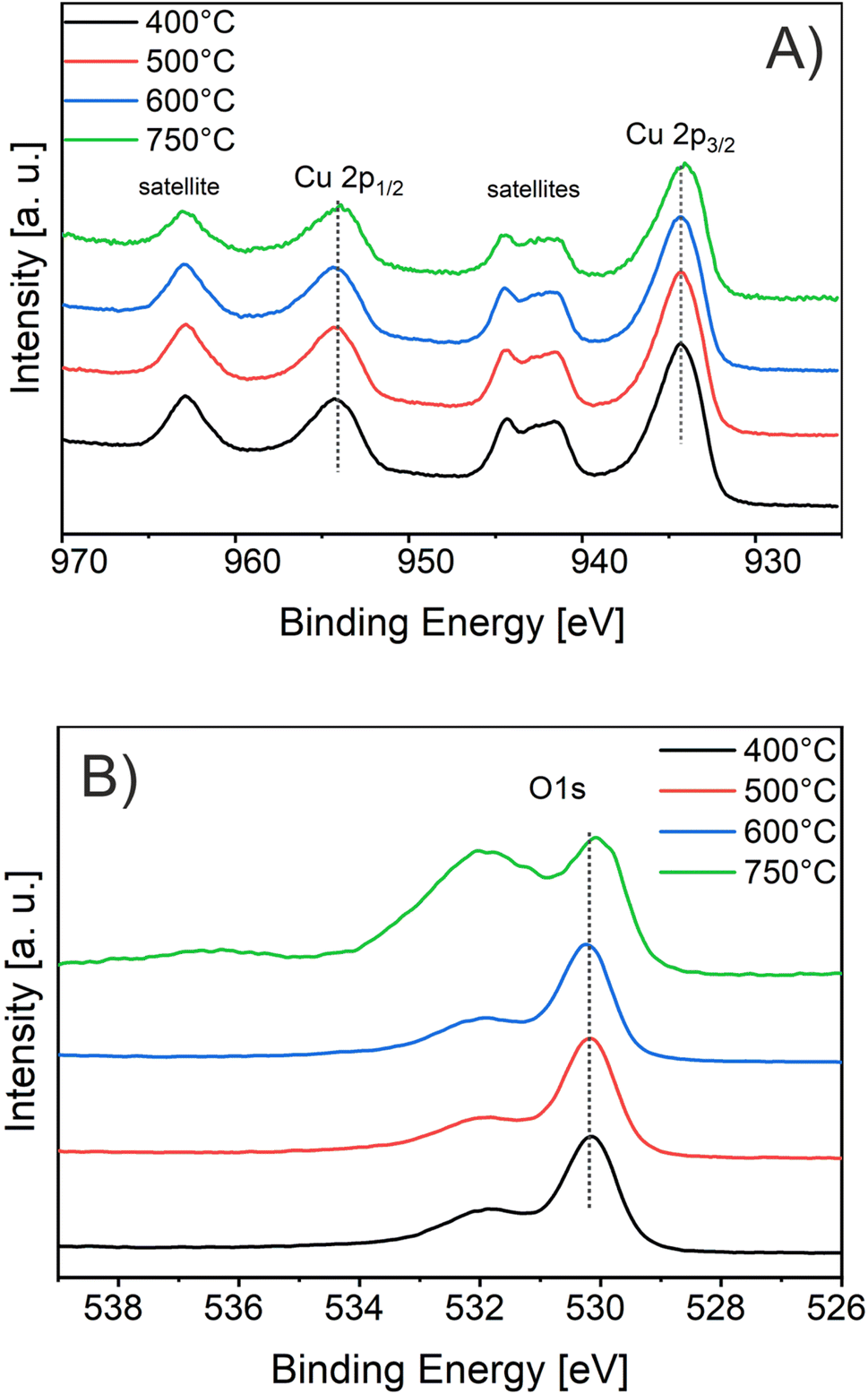 | ||
| Fig. 4 (A) XP spectra of the Cu 2p1/2 and Cu 2p3/2 core levels and (B) the O 1s photoemission of the mesoporous CuO-400, CuO-500, CuO-600, and CuO-750 samples. | ||
Optoelectronic and photoelectrochemical characterization
UV/Vis spectroscopy was conducted to evaluate the absorbance spectra of the CuO photocathodes. As presented in Fig. S6,† the absorbance spectra of all four samples analyzed between 400 nm and 1300 nm exhibited strong absorption in the visible spectrum of light. Photographs taken exemplarily from the CuO-600 sample (Fig. 5A) visualize that the thin films were crack-free (even on the milli- and centimeter scale) and optically transparent, an important finding since this proves successful fabrication of high-quality and reproducible materials. Of note, optically transparent thin films readily available on transparent conductive substrates are of great interest for application in (PEC) tandem cells, as transmission is ensured by the top-absorber, which is not possible with optically turbid films scattering the incident light. Especially, CuO has been shown to absorb large portions of the solar spectrum owing to its low indirect band gap energy.29 CuO-400, CuO-500, and CuO-600 thin films do not demonstrate a significant difference in their capability to absorb photons, suggesting that the thermally induced increase of crystallinity from 400 °C to 600 °C does not considerably affect the optical characteristics of these CuO samples. However, the CuO-750 thin film shows an increased absorbance compared to the other samples, especially in the visible wavelength region between 900 nm and 500 nm. This observation can be most likely assigned to the morphological differences of the bulk structures (larger nanodomains as observed in Fig. 2), which also affects the electronic structure of the CuO-750, leading to a distinct optical absorption behavior. Additionally, the film thickness of CuO-750 was determined to be 300 nm by profilometry, which is an increase of about 20% compared to the film thicknesses of the CuO samples calcined at lower temperature (average 250 nm). Hence, this effect also contributes to the enhanced absorption in the visible wavelength range. To determine the indirect band gap energy of the CuO samples, Tauc plots were derived from the absorbance spectra. CuO is known to be an indirect semiconductor and for nanostructured CuO typical band gap energies were reported between 1.2 to 1.7 eV.29 Here, (αhν)1/2 was plotted, assuming an indirect optical transition, against the photon energy hν (Fig. 5B). Accordingly, by linear extrapolation of the data points, the indirect band gap energies were determined to be between 1.3 eV and 1.4 eV for all CuO samples. These values are in accordance with literature.29,38,51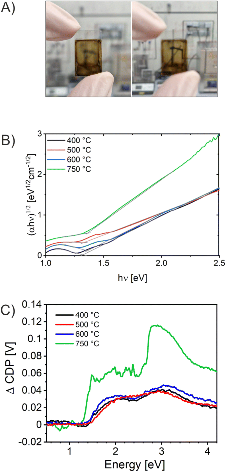 | ||
| Fig. 5 (A) Photograph of the CuO-600 thin film on FTO in focus (left) and defocused (right). (B) Tauc-plots assuming an indirect optical transition. (C) Surface photovoltage spectroscopy analyzed for the mesoporous CuO-400, CuO-500, CuO-600, and CuO-750 photocathodes. The spectral shape is modulated by the intensity output of the Xe-lamp/monochromator configuration.84 | ||
In order to further investigate the ability of the CuO films to generate and separate charge carriers under illumination, Vibrating Kelvin Probe-Surface Photovoltage Spectroscopy (VKP-SPS) was applied to the nanoporous CuO films exposed to air. VKP-SPS measures the contact potential difference (CPD) change of a sample in the dark and under illumination. The difference defines the surface photovoltage signal: SPV = CPD (light) − CPD (dark). The SPV is equal or similar to the photovoltage of the photoelectrode.84–88 The photovoltage defines the maximum electrochemical work that can be performed by an electrode under illumination. SPV spectra of the various samples are compared in Fig. 5C. All CuO samples present positive CPD signals corresponding to the movement of photoexcited electrons toward the Kelvin probe and of holes toward the conductive back contact. The charge transfer direction (electrons to the CuO surface) is typical of p-type semiconductor photocathodes, such as p-CuBi2O4, and indicates that charge carriers are separated by a depletion region at the CuO surface.89 The photo-onset of the CPD signal is a measure of the band gap of the material. It occurs at 1.4 eV for CuO-400, CuO-500, and CuO-600 and at 1.3 eV for CuO-750. This correlates well with the indirect optical transition energies seen in the UV-Vis spectra (found between 1.3 eV and 1.4 eV) and suggests the absence of optically active defects within the CuO bandgap. Qualitatively, these SPV data are similar to those reported by Xing et al., for CuO films made by electrodeposition.90 The maximum SPV signals were observed at ∼3.0 eV as a result of the higher light intensity of the Xe lamp at this energy. Photovoltage values at 2 eV are 30 mV, 30 mV, 34 mV, and 60 mV for CuO-400, CuO-500, CuO-600, and CuO-750, respectively. This trend agrees with the photocurrent behavior of the photoelectrodes at 0.3 V vs. RHE (Fig. 6C), which shows increasing photocurrent in the order CuO-400 < CuO-500 < CuO-600 <<< CuO-750. The increased photovoltage of the CuO-750 film is attributed to its 20% increased thickness, which allows for better photon absorption.91 Schottky barriers at the ITO/FTO-CuO interface as seen recently for p-CuGa3Se5 (ref. 84) or CuFe2O4 photoanodes55 appear not to be a limiting factor.
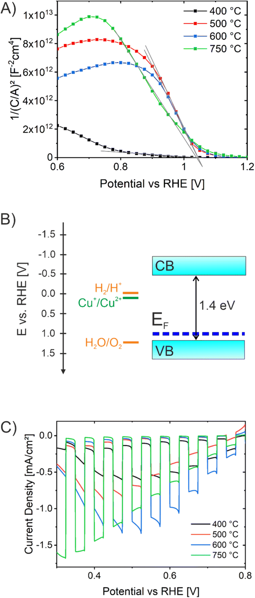 | ||
| Fig. 6 (A) Mott–Schottky analysis and (B) energy band diagram of mesoporous CuO photocathodes based on the energy band gap determined by UV/Vis spectroscopy and the flat band potential derived by Mott–Schottky analysis. (C) Chopped-light voltammetry analysis of mesoporous CuO-400, CuO-500, CuO-600, and CuO-750 photocathodes. Experiments were conducted in aqueous electrolyte containing 0.2 M Na2SO4, a phosphate buffer, and 1 M Na2SO3 utilizing a white light LED (100 mW cm−2). | ||
Mott–Schottky (MS) analyses were carried out for CuO-400, CuO-500, CuO-600, and CuO-750 (Fig. 6A) in order to determine majority carrier type and flat band potential. Firstly, the negative slopes clearly indicate the p-type character of all CuO samples. The CuO-400 sample showed much smaller 1/C2 values compared to the higher temperatures, also indicated by a smaller slope in the linear region. This is related to a lower degree of crystallinity in these films, which affects the capacitance of the investigated photoelectrode, and was also observed for other CuO nanostructures annealed at comparably low temperatures.51 The flat band potential is an important PEC parameter which directly reflects the thermodynamic ability of a semiconductor to perform redox reactions at its surface. It provides the Fermi energy (EF) of CuO. Because holes are the majority carriers, EF can be used to approximate the valence band edge. The flat band potential was analyzed to be located at 1.0 V vs. RHE independent of the calcination temperature, giving rise to the assumption that the position of the conduction band (CB) in nanoporous CuO was not significantly affected by the annealing procedure. The determined flat band potentials are in agreement with literature.29 Assuming an indirect band gap energy of 1.4 eV as derived by the Tauc plots (Fig. 5B), the corresponding energy diagram can be drawn as visualized in Fig. 6B. Since the conduction band lies energetically above the hydrogen evolution potential (0 V vs. RHE), it can be stated that the electrons in the CB are theoretically able to reduce protons to hydrogen, but the holes from the valence band are not capable of oxidizing water to oxygen without applying an external bias.
To study the photoelectrochemical activity of the nanocrystalline and porous CuO photocathodes as related to their annealing temperature, the photocurrent response of CuO-400, CuO-500, CuO-600, and CuO-750 were investigated under intermittent/chopped light (white light LED, light period time 10 s) in 0.2 M Na2SO4 and 1.0 M Na2SO3 (Fig. 6C). All CuO thin films were found to exclusively show negative photocurrent densities under illumination, in agreement with their p-type properties and behavior as photocathodes. When comparing the photocurrent responses of the four CuO samples, CuO-750 shows the highest photocurrent density of −1.7 mA cm−2 at 0.32 V vs. RHE, followed by −1.35 mA cm−2 for CuO-600, −0.90 mA cm−2 for CuO-500, and −0.61 mA cm−2 for CuO-400 at 0.52 V vs. RHE. This trend agrees with the surface photovoltage behavior of the photoelectrodes as discussed above. This suggest that the higher the annealing temperature of the nanoporous CuO thin films, the better the photoelectrochemical properties. The data imply that the CuO films are not photostable and photodegradation is already initiated within the first measurement cycle. In subsequent scans, a significant decay of the photocurrent is observed (see Fig. S7A†). The self-corrosion and detachment of the CuO thin films is also demonstrated by SEM after PEC characterization (see Fig. S7B†) showing the visibility of pristine FTO crystals from the substrate.
Interestingly, the photocurrent responses of the CuO samples calcined between 400 °C and 600 °C exhibit photocurrent transients when the light is turned on, which is most prominent for CuO-600 °C. These spikes could either indicate trapping and recombination processes of the photoexcited electron–hole pairs at surface states92–94 and/or photocorrosion processes taking place at the CuO surface. The CuO-750 sample demonstrated the lowest surface area (determined by Kr-physisorption) and consequently possesses the lowest concentration of grain boundaries, which in turn provides fewer surface states and could therefore explains the suppressed transients. A high crystallinity, a good connectivity of the nanoporous network, and lower surface areas seems vital for sufficient electric conductivity allowing for efficient transfer of the charge carriers from their point of excitation to the CuO-electrolyte interface. These observations were in good agreement with a temperature-dependent study on CuO nanofibers prepared by electrospinning. That study demonstrated the benefit of larger CuO domains with low surface area (1 cm2 g−1) for allowing charge carrier migration, owing to a decreased concentration of surface defects at grain boundaries.51 As demonstrated in Fig. 1 and 2, the CuO-750 thin films are composed of much larger nanocrystalline domains (14 nm) compared to the nanocrystals grown at lower calcination temperatures (9 nm). In principle, smaller nanoparticles possess an increased concentration of grain boundaries, which act as recombination sites for charge carriers as they diffuse and drift from the site of photoexcitation to the semiconductor–electrolyte interface. As a consequence, the photocurrent density is a function of annealing temperature, since the increase in annealing temperature results in the growth and development of larger nanoparticular domains, containing fewer (structural) bulk and surface defects due to increased crystallinity and lower surface areas, respectively. Additionally, the increased photoresponse of CuO-750 has to be partially assigned to the ca. 20% increased film thickness leading to enhanced absorption of visible-light photons. In essence, the photoelectrochemical performance of the nanoporous CuO-750 thin film photocathodes can be ascribed to four control parameters: the degree of crystallinity, dimensions of nanodomains, the surface area, and the film thickness.
Incident-photon-to-current efficiency (IPCE) analysis (see Fig. S8†) was performed to confirm the results obtained by chopped-light voltammetry (CLV). The IPCE data demonstrate the same activity dependency on calcination temperature as observed for the attained photocurrents: with increasing annealing temperature the IPCE value increases from 4.9% for CuO-400 to 14.7% for CuO-600 measured at an excitation wavelength of 369 nm (with a monochromatic light source) and at 0.4 V vs. RHE. Especially in the ultraviolet range (below 400 nm), the quantum efficiency showed the most pronounced difference for distinct annealing temperatures. The IPCE data of CuO-750 was not comparable to the other samples since the ITO-coated quartz substrates used for this film reflected the incident light to a much larger extent by backside illumination compared to the FTO-substrates. Therefore, CuO-600 was chosen as control sample for any further PEC characterization to ensure better comparability. The measured IPCE values of CuO thin films are rather high when compared to similar sol–gel-derived nanostructures, such as in the study of Uchiyama et al.,42 achieving only 8.7% IPCE efficiency at 300 nm excitation wavelength. It is noteworthy that these nanoporous CuO thin films were also prepared by dip-coating and subsequent annealing at 600 °C and possess identical film thickness of 220 nm, which allows for direct comparison of the photoelectrochemical properties. The authors attributed the good photoelectrochemical performance to the large surface area arising from the highly porous structure (which was varied during sol–gel synthesis by adding distinct concentrations of poly vinyl pyrrolidone).42
In order to examine how much of the observed photocurrent densities originates from hydrogen production, gas chromatography measurements were performed while the photoelectrode was at 0.35 V vs. RHE and under illumination with AM 1.5 simulated sunlight. No hydrogen was observed within the error of the experiment (1 µmol), which means that all of the photocurrent can be attributed to self-reduction of CuO. During the course of the 20 min experiment, the photocurrent was found to decline to less than 20 µA cm−2 after 1000 s (Fig. S9†). The photocorrosion is a consequence of the electrochemical instability of CuO especially at potentials below 0.15 V vs. RHE,95 where reduction of Cu2+ to Cu+ cations occurs in competition with proton reduction.30,96
Next, the contribution of oxygen reduction was also investigated by comparing the photoresponse of illuminated CuO-600 samples in a nitrogen (N2)- and oxygen (O2)-bubbled electrolyte, respectively. The CuO-600 photocathodes analyzed in the N2-purged electrolyte showed a 0.09 mA cm−2 increased photocurrent density at 0.55 V vs. RHE compared to the photocathodes measured in the O2-bubbled electrolyte (see Fig. S10†). This shows that oxygen reduction at the working electrode does not contribute significantly to the measured photocurrent density (from Fig. 6C). On the contrary, O2 appears to reduce the photocurrent. This is ascribed to decreased band bending at the CuO/O2/H2O interface, which is a result of the positive O2/H2O reduction potential (1.23 V vs. RHE), which favors an ohmic contact with CuO (EF ≈ 1.0 eV).
To investigate if the CuO films can reduce the fast electron transfer reagent methyl viologen (MV, E0 = −0.03 VRHE at pH 7),84 PEC scans were repeated in 0.01 M MVCl2 with 0.05 M sodium phosphate buffer (Fig. S11†). Photocurrent densities above 1.0 mA cm−2 at 0.32 V vs. RHE can be seen for the CuO-600 film (with the other films showing lower activity), similar to what was seen in sodium sulfate electrolyte. However, over time the photocurrent again decays (Fig. S12†) as a result of the self-reduction of the CuO reaching a steady-state value of about 40 µA cm−2. This shows that CuO is intrinsically unstable under illumination in aqueous media.
Film thickness investigations
Since the layer-by-layer deposition of films on conductive substrates was reported to enhance the crystallization behavior of metal oxide nanostructures resulting in improved photoactivity,59,97 multiple dip-coating cycles including stabilization steps for 30 min at 250 °C were conducted. In general, the optimum film thickness of metal oxide photoelectrodes depends on the minority charge carrier diffusion length and light penetration depth at a specific wavelength. For example, hematite is known to possess an ultrashort minority charge carrier diffusion length of merely 2–4 nm; however, the absorption coefficient is 120 nm at 550 nm wavelength.98 Therefore, the attempt to shorten the diffusion path by preparation of ultrathin hematite films merely 12.5 nm in thickness did not lead to the desired enhancement in photoactivity since an insufficient amount of photons were absorbed.40 However, the charge carrier diffusion length/mobility is not an intrinsic material property allowing for prediction of the ideal film thickness, since it has been reported that also the synthesis procedure impacts the crystallinity (= conductivity) and/or the formation of oxygen vacancies of the sample, so no standardized/optimized film thickness with respect to light absorption is available for CuO.29 The dependency of optimized transport distances of charge carriers on the annealing temperature of sol–gel films was demonstrated, for example, for ZnFe2O4.99The dip-coating steps/cycles (referred to as layers) were carried out from one to five times, resulting in the formation of CuO thin films with distinct thicknesses ranging from 170 ± 20 nm to 490 ± 20 nm as summarized in Table S3.† The film thickness was determined by profilometry. The development of the film thickness as a result of the number of CuO layers is illustrated in Fig. 7A. In principle, it can be stated that the film thickness increases with the number of CuO layers.
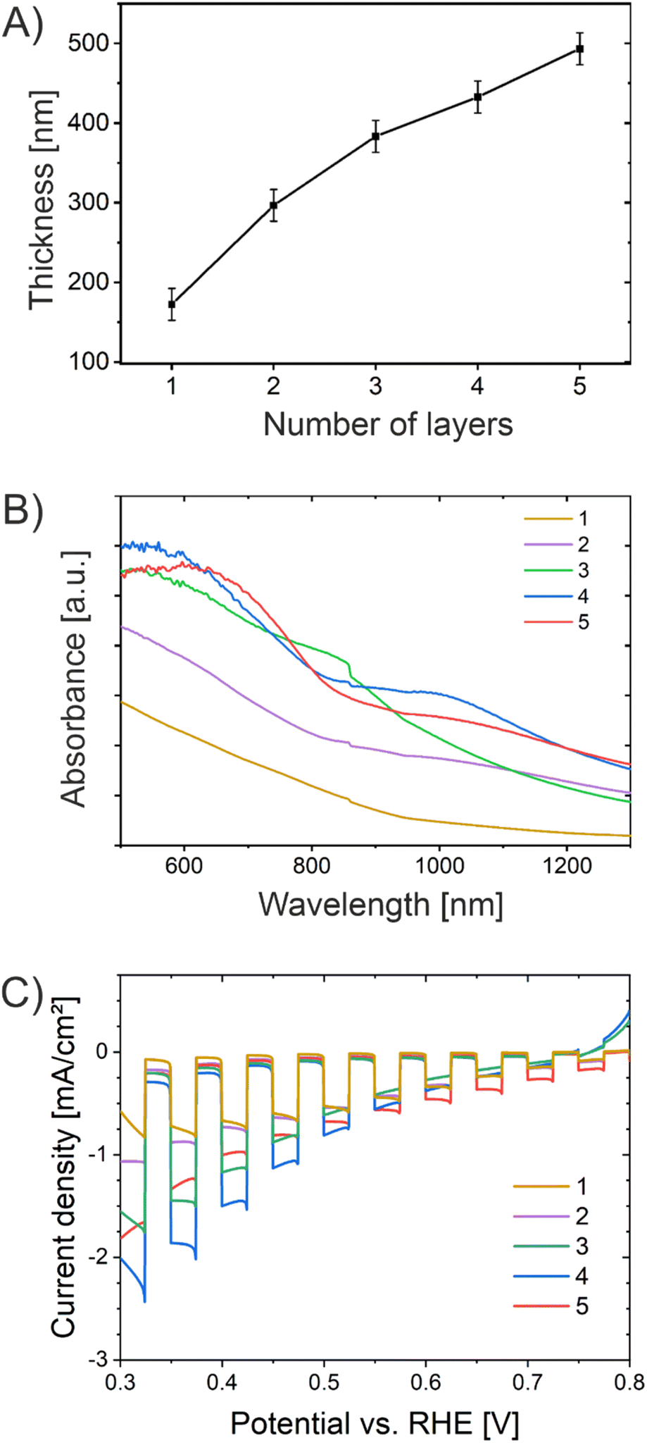 | ||
| Fig. 7 (A) Development of the film thickness of CuO-600 samples prepared by multiple dip-coating steps from one to five. (B) Absorbance spectra of the multilayered CuO-600 films. (C) Chopped-light voltammetry recorded for CuO-600 with varied film thicknesses with a white light LED (100 mW cm−2, light period time 10 s) in 0.2 M Na2SO4 and 1 M Na2SO3. | ||
Fig. 7B presents the UV/Vis absorbance spectra of the CuO films prepared by multiple dip-coating steps measured between 500 nm and 1300 nm. The absorbance increases steadily from one to four CuO thin film layers. After 4 layers, the absorption characteristics do not change substantially, which can most likely be ascribed to the fact that the thickness of the thin film only increases about 60 nm from the fourth to the fifth layer, resulting in no additional absorptivity. The CLV curves of CuO samples with multiple layers (one to five) are shown in Fig. 7C. The photocurrent density was determined to be a function of the number of CuO layers, and thus of the film thickness. Owing to an increased film thickness, more photons can be absorbed by the CuO photocathode, resulting in a larger amount of photogenerated electron–hole pairs (excitons) migrating towards the CuO-electrolyte interface (to perform photoreduction) and the back contact, respectively.
The sample with four CuO layers revealed the highest photocurrent density of −2.4 mA cm−2 at 0.32 V vs. RHE, which even exceeded the value obtained for the sample with five layers. If the migration distance becomes too large related to the diffusion length of the electrons, as in the case of five CuO-layers, they recombine at bulk and surface defects before collection/redox reaction can occur. In conclusion, the sample with four CuO layers, with a thickness of 430 ± 20 nm, has been shown to possess the optimum film thickness in terms of light absorption, charge carrier separation, and drift/diffusion distances. The optimum film thickness attained in this work is close to the values determined by Kyesmen et al., reporting an optimum thickness of 419 nm for wet-chemically processed and structurally related CuO photocathodes.59 In contrast, optimum thicknesses of 230 nm (ref. 42) and 500 nm (ref. 100) have also been reported, although applying different preparation techniques, thus allowing the conclusion that the optimum thickness/nanostructure of CuO cathodes strongly depends on the synthesis procedure leading to distinct morphologies and degrees of crystallinity. Even though the decay of the photocurrent density of the five-layered CuO film was found to be occurring on a slower time scale (from seconds to minutes), the sample also started to suffer from corrosion after the third PEC analysis cycle (Fig. S13†). In essence, the increased photocurrents have to be also assigned to photoreduction as discussed before.
Conclusion
In this work, macro-/mesoporous CuO thin films were produced via a sol–gel based dip-coating technique making use of the EISA process. Based on the development of a novel synthesis route, nanocrystalline and nanostructured CuO samples were prepared at distinct annealing temperatures (400 °C, 500 °C, 600 °C, and 750 °C) to study the impact of the nanostructure, surface area, and crystallinity on the physicochemical and photoelectrochemical properties. The obtained CuO thin films possess structurally intact nanoporous frameworks and were homogeneous and crack-free not only on the meso- but also on the macroscale. The morphology and nanostructure were investigated by means of SEM, TEM, GI-XRD, XPS, and Raman spectroscopy which could consistently prove a pure CuO phase crystallizing in the monoclinic structure in the absence of any side phases and impurities. The CuO materials showed indirect optical band gap energies of 1.3–1.4 eV, which corresponded well to the band gaps measured by surface photovoltage spectroscopy (SPV). All films are p-type and produce cathodic photocurrent when in contact with aqueous electrolytes containing either Na2SO4 or methyl viologen as a fast electron acceptor. The highest achieved photocurrent density of −2.4 mA cm−2 at 0.32 V vs. RHE was recorded for a four-times coated CuO film, which had an optimum thickness of 430 nm in terms of light absorption and charge carrier transport distances. However, no hydrogen evolution is observed and photocurrents decay over the course of 20–30 min as a result of photocorrosion. This shows that CuO is unstable when illuminated in aqueous electrolytes and will require protection layers and/or co-catalysts to achieve stable photocathode performance. This is a challenge to be addressed in future work.Experimental section
Materials
All used chemicals were of analytical grade. Cu(NO3)2 × 2.5H2O, Pluronic® F-127 were obtained from Sigma Aldrich and used as received. 2-Methoxyethanol (2-ME; ≥99.5%) and ethanol (≥99.8%) was obtained by Roth and used as received.Synthesis
For the synthesis of mesoporous copper oxide thin films, fluorine-doped tin oxide (FTO)-coated glass, indium-doped tin oxide (ITO)-coated quartz glass (from Präzisions Glas & Optik) or silicon (100) wafer (from Siltronic) were used as substrates. The substrates were cleaned in a 50/50 mixture by volume of ethanol and acetone in an ultrasonic bath for 15 minutes.For a typical synthesis batch, 384 mg Cu(NO3)2 × 2.5H2O was dissolved in 0.7 mL 2-methoxyethanol and homogenized with a shaker. In a separate solution, 45 mg Pluronic® F-127 (structure-directing agent) was dissolved in 0.7 mL 2-methoxyethanol. After complete dissolution of the precursors, both solutions were mixed dropwise. In the next step, 0.8 mL of ethanol and 0.1 mL of distilled water was added to the precursor solution, and the solution was stirred for 30 minutes. Dip-coating was conducted at 16–19% relative humidity and the samples were dried for about 4 minutes in the dip-coating chamber. Then, the samples were transferred to a furnace preheated to 125 °C. The samples were dried at 125 °C for a minimum of 15 minutes before the heating procedure was started (see Fig. S14†). The amorphous samples were heated up to 250 °C with a heating rate of 1 °C min−1 and held for 24 hours. The temperature of the furnace was increased to the desired calcination temperature (400 °C, 500 °C, 600 °C or 750 °C) with a heating rate of 5 °C min−1 and held for 2 hours. For annealing at 400 °C, 500 °C, and 600 °C FTO glasses were used, whereas for 750 °C ITO-coated quartz was utilized as substrate.
For the optimization of the film thickness, substrates were dipped multiple times into the dip-coating solution. The substrates were immersed into the dip-coating solution at 16–19% RH with a withdrawal speed of 2 mm s−1 and placed afterwards into the pre-heated furnace at 250 °C for 30 minutes. This procedure was repeated until samples with up to 5 layers were attained. Subsequently, all samples were held at 250 °C for 24 h, heated up to 600 °C with a heating rate of 5 °C h−1 and held at 600 °C for 2 h (as shown in Fig. S14†).
Structural and optical characterization
Grazing-incidence X-ray diffraction was carried out with a Rigaku Smartlab instrument which uses copper Kα radiation applying 20 kV and 170 mA for analysis. A 2Θ range between 20° and 80° was scanned with a scan rate of 2° per minute and with °5 incident angle of X-rays to the surface of the thin film. For the calculations of crystallite sizes by the Williamson–Hall method,74 the full-width at half-maximum (FWHM) times cos(Θ) was plotted over 4 times sin(Θ) applied for the (110), (202), and (004) peaks. The intercept of the linear fit with the y-axis provides the crystallite size. To attain the FWHM, the background was subtracted. The wavelength of the X-ray beam was λ = 1.54 Å. The crystallographic structure model was compiled with the VESTA software. For Raman spectroscopy, a Horiba HR800 Raman microscope was utilized. The excitation wavelength was 514 nm. Prior to measurement of the mesoporous CuO thin films on Si substrates, the calibration was accomplished with the same, bare, silicon substrates as reference. For all samples, analyses were conducted on several spots to ensure reproducibility. X-ray photoelectron spectroscopy (XPS) was conducted at the DAISY Bat (Darmstadt Integrated System for Battery Research), consisting of a PHI VersaProbe II Scanning ESCA Microprobe (Physical Electronics) with base pressure of <10−7 Pa. For XPS, monochromatic Al Kα radiation with an energy of 1486.6 eV was used; the anode was operated at a power of 50 W. For detail spectra, the pass energy was set to 23.5 eV with a step size of 0.1 eV for detail scans and to a pass energy of 187.6 eV for survey scans. Binding energy calibration was performed regularly by setting the Au 4f7/2 emission of Au foil to 84.00 eV. XPS investigations could not be performed on 1 cm2 ITO-coated quartz substrates (necessary dimensions of the substrate for XPS analysis) for the CuO-750 sample due to insufficient adhesion of the dip-coating solution on these small substrates. Hence, larger ITO substrates were mechanically broken into smaller pieces for XPS investigation. SEM was carried out at a Philips XL 30 electron microscope applying an acceleration voltage of 30 kV at a working distance of 10 mm. For all samples different spots were investigated to ensure that the data are representative for the whole sample. The film thicknesses of the mesoporous CuO samples were evaluated by a profilometer (Bruker Dektak XT) with a scan speed of 10 µm s−1. Krypton physisorption measurements were conducted at 77 K by an ASiQ-MP-MP-AG setup (Anton Paar QuantaTec, Boynton Beach, USA). The saturation pressure p0 was kept constant at 2.63 Torr. Prior to the measurements, the samples were degassed for 12 h at 120 °C in vacuum. The data analysis was carried out using the BET model via software ASiQwin (Anton Paar QuantaTec, Boynton Beach, USA), while the sample weight was determined by the film thin area, thin film thickness (values of the profilometry measurements), and an assumed porosity of 30%. For TEM investigations, particles were scratched off from the substrates, dispersed in ethanol, and treated with ultrasonication. A droplet of the dispersion was deposited on a carbon-coated copper grid (holey type, Plano GmbH, Wetzlar) and allowed to dry. To avoid charging under the electron beam, the grid was coated with a thin carbon film (carbon coater MED 010, Bal-Tec AG, Balzers, Liechtenstein). Finally, the sample was examined in a FEG TEM (JEM2100F, JEOL Ltd., Tokyo, Japan). EDS maps were recorded using an Oxford X-Max 80 EDS detector.Electrochemical measurements
The electrochemical measurements were carried out using a Zahner cell with a three-electrode setup and a platinum wire as counter electrode. The mesoporous CuO thin films were used as working electrode. An Ag/AgCl electrode stored in 3 M NaCl was used as reference electrode.All three electrodes were immersed in the electrolyte, which was an aqueous solution containing 0.2 M Na2SO4, 0.1 M KH2PO4 and 0.1 M K2HPO4 acting as buffer, and 1 M Na2SO3. Before starting the photoelectrochemical measurements, the Ag/AgCl reference electrode was measured against the reversible hydrogen electrode in the described electrolyte. The voltage empirically obtained was 653 ± 5 mV and was in good accordance with the theoretical value of 655 mV determined by the Nernst equation (pH 7.8). For the chopped-light voltammetry (CLV) the Zahner cell was placed in front of a white LED with a light intensity of 100 mW cm−2. The applied bias was regulated by a ZENNIUM PRO potentiostat scanning from 0.85–0.3 V vs. RHE with a scan rate of 5 mV s−1. The switching time between light “on” and “off” was set to 10 seconds. Mott–Schottky measurements in the dark were applied to identify the flat band potential of the material analyzed between 0.6–1.2 V vs. RHE with a frequency of 100 Hz and an amplitude of 5 mV. The flat band potential was determined by using the Mott–Schottky equation and graphical fitting of the linear part of the plot, thus identifying the intercept with the x-axis. For the incident photon-to-current efficiency (IPCE) measurement, a tunable light source (TSL03 from Zahner) was used (wavelengths, FWHM, and power of the LEDs are shown in Table S2 in the ESI†). The samples were illuminated from the backside. The applied voltage was 400 mV vs. RHE, and the frequency was 1 Hz.
Photoelectrochemical measurements under AM 1.5 illumination were conducted using a Gamry Reference 600 Potentiostat connected to a typical three-electrode system, with a Pt counter electrode and a calomel reference electrode (3.5 M KCl). Measurements were performed with continuous N2 purging in either in 1.0 M Na2SO3/0.2 M Na2SO4 electrolyte or in 0.01 MVCl2 (methylviologen dichloride) with 0.05 M sodium phosphate buffer (pH = 7) at a scan speed of 10 mV s−1 in cathodic direction. Potentials were converted to the normal hydrogen electrode (NHE) by calibration in 10 mM K3Fe(CN)6/K4Fe(CN)6 and adjusted to RHE using the equation VRHE = VNHE + 0.0592 × pH.
Surface photovoltage spectra were measured using a circular (2.5 mm diameter), semitransparent vibrating gold mesh disk (Kelvin Probe S, Besocke Delta Phi) controlled by a Kelvin Control 7 Oscillator/amplifier (Besocke Delta Phi), and mounted inside of a home-built vacuum chamber open to air. Samples were placed 1.0 mm underneath the Kelvin probe and contacted electrically to ground. Illumination was provided by a 300 W Xe lamp and filtered through an Oriel Cornerstone 130 monochromator. The intensity at the sample was 50 µW cm−2 in the 0.8–3.6 eV interval. The light exiting the monochromator had a FWHM (full-width/half-maximum) of 8–15 nm. Spectra were acquired by stepping the photon energy by 0.0124 eV every 5 seconds and by measuring the contact potential difference (CPD) value at each step. All ΔCPD values are reported relative to the CPD value in the dark. Positive values correspond to electrons moving towards the Kelvin probe and negative values correspond to electrons moving away from the Kelvin probe.
Conflicts of interest
There are no conflicts to declare.Acknowledgements
ME acknowledges both the Deutsche Forschungsgemeinschaft (DFG, German Research Foundation, Walter Benjamin Program to M. Einert) with project no. 469377211 and the Federal Ministry of Education and Research (BMBF) within the project TWOB under Award Number 033RC036 for financial support. JPH and MM acknowledge DFG for funding under project no. 416542991. Support for surface photovoltage spectroscopy measurements was provided by the U.S. Department of Energy, Office of Science, Office of Basic Energy Sciences under Award Number DOE-SC0015329.References
- L. J. Minggu, W. R. W. Daud and M. B. Kassim, An overview of photocells and photoreactors for photoelectrochemical water splitting, Int. J. Hydrogen Energy, 2010, 35, 5233–5244 CrossRef CAS.
- M. S. Prévot and K. Sivula, Photoelectrochemical tandem cells for solar water splitting, J. Phys. Chem. C, 2013, 117, 17879–17893 CrossRef.
- B. Turan, J.-P. Becker, F. Urbain, F. Finger, U. Rau and S. Haas, Upscaling of integrated photoelectrochemical water-splitting devices to large areas, Nat. Commun., 2016, 7, 12681 CrossRef PubMed.
- K. Sivula and R. van de Krol, Semiconducting materials for photoelectrochemical energy conversion, Nat. Rev. Mater., 2016, 1, 1–16 Search PubMed.
- W. Yang, R. R. Prabhakar, J. Tan, S. D. Tilley and J. Moon, Strategies for enhancing the photocurrent, photovoltage, and stability of photoelectrodes for photoelectrochemical water splitting, Chem. Soc. Rev., 2019, 48, 4979–5015 RSC.
- A. Fujishima and K. Honda, Electrochemical photolysis of water at a semiconductor electrode, Nature, 1972, 238, 37–38 CrossRef CAS PubMed.
- P. J. Boddy, Oxygen evolution on semiconducting TiO2, J. Electrochem. Soc., 1968, 115, 199 CrossRef CAS.
- R. van de Krol, Y. Liang and J. Schoonman, Solar hydrogen production with nanostructured metal oxides, J. Mater. Chem., 2008, 18, 2311–2320 RSC.
- M. G. Walter, E. L. Warren, J. R. McKone, S. W. Boettcher, Q. Mi, E. A. Santori and N. S. Lewis, Solar water splitting cells, Chem. Rev., 2010, 110, 6446–6473 CrossRef CAS PubMed.
- F. E. Osterloh, Inorganic materials as catalysts for photochemical splitting of water, Chem. Mater., 2008, 20, 35–54 CrossRef CAS.
- F. E. Osterloh, Inorganic nanostructures for photoelectrochemical and photocatalytic water splitting, Chem. Soc. Rev., 2013, 42, 2294–2320 RSC.
- I. Roger, M. A. Shipman and M. D. Symes, Earth-abundant catalysts for electrochemical and photoelectrochemical water splitting, Nat. Rev. Chem., 2017, 1, 3 CrossRef CAS.
- W. Yang and J. Moon, Recent advances in earth‐abundant photocathodes for photoelectrochemical water splitting, ChemSusChem, 2019, 12, 1889–1899 CrossRef CAS PubMed.
- S. Corby, R. Rao, L. Steier and J. Durrant, The kinetics of metal oxide photoanodes from charge generation to catalysis, Nat. Rev. Mater., 2021, 6, 1136–1155 CrossRef CAS.
- A. G. Tamirat, J. Rick, A. A. Dubale, W.-N. Su and B.-J. Hwang, Using hematite for photoelectrochemical water splitting: a review of current progress and challenges, Nanoscale Horiz., 2016, 1, 243–267 RSC.
- M. Einert, R. Ostermann, T. Weller, S. Zellmer, G. Garnweitner, B. M. Smarsly and R. Marschall, Hollow α-Fe2O3 nanofibres for solar water oxidation: improving the photoelectrochemical performance by formation of α-Fe2O3/ITO-composite photoanodes, J. Mater. Chem. A, 2016, 4, 18444–18456 RSC.
- M. Ma, K. Zhang, P. Li, M. S. Jung, M. J. Jeong and J. H. Park, Dual oxygen and tungsten vacancies on a WO3 photoanode for enhanced water oxidation, Angew. Chem., 2016, 128, 11998–12002 CrossRef.
- M. Ade, L. Schumacher and R. Marschall, Seed layer formation determines photocurrent response of hydrothermally-grown WO3 photoanodes, Sustainable Energy Fuels, 2023, 7, 4332–4340 RSC.
- G. Wang, H. Wang, Y. Ling, Y. Tang, X. Yang, R. C. Fitzmorris, C. Wang, J. Z. Zhang and Y. Li, Hydrogen-treated TiO2 nanowire arrays for photoelectrochemical water splitting, Nano Lett., 2011, 11, 3026–3033 CrossRef CAS PubMed.
- M. Einert, P. Hartmann, B. Smarsly and T. Brezesinski, Quasi-homogenous photocatalysis of quantum-sized Fe-doped TiO2 in optically transparent aqueous dispersions, Sci. Rep., 2021, 11, 17687 CrossRef CAS PubMed.
- X. Yang, A. Wolcott, G. Wang, A. Sobo, R. C. Fitzmorris, F. Qian, J. Z. Zhang and Y. Li, Nitrogen-doped ZnO nanowire arrays for photoelectrochemical water splitting, Nano Lett., 2009, 9, 2331–2336 CrossRef CAS PubMed.
- J. Jian, Y. Xu, X. Yang, W. Liu, M. Fu, H. Yu, F. Xu, F. Feng, L. Jia and D. Friedrich, Embedding laser generated nanocrystals in BiVO4 photoanode for efficient photoelectrochemical water splitting, Nat. Commun., 2019, 10, 2609 CrossRef PubMed.
- X. Wu, F. E. Oropeza, Z. Qi, M. Einert, C. Tian, C. Maheu, K. Lv and J. P. Hofmann, Influence of Mo doping on interfacial charge carrier dynamics in photoelectrochemical water oxidation on BiVO4, Sustainable Energy Fuels, 2023, 7, 2923–2933 RSC.
- F. E. Oropeza, B. T. Feleki, K. H. L. Zhang, E. J. M. Hensen and J. P. Hofmann, Influence of Reduced Cu Surface States on the Photoelectrochemical Properties of CuBi2O4, ACS Appl. Energy Mater., 2019, 2, 6866–6874 CrossRef CAS.
- F. E. Oropeza, N. Y. Dzade, A. Pons-Martí, Z. Yang, K. H. L. Zhang, N. H. de Leeuw, E. J. M. Hensen and J. P. Hofmann, Electronic Structure and Interface Energetics of CuBi2O4 Photoelectrodes, J. Phys. Chem. C, 2020, 124, 22416–22425 CrossRef CAS PubMed.
- C. Lohaus, A. Klein and W. Jaegermann, Limitation of Fermi level shifts by polaron defect states in hematite photoelectrodes, Nat. Commun., 2018, 9, 4309 CrossRef PubMed.
- Y. Chen, X. Feng, Y. Liu, X. Guan, C. Burda and L. Guo, Metal oxide-based tandem cells for self-biased photoelectrochemical water splitting, ACS Energy Lett., 2020, 5, 844–866 CrossRef CAS.
- Z. Wang, L. Zhang, T. U. Schülli, Y. Bai, S. A. Monny, A. Du and L. Wang, Identifying copper vacancies and their role in the CuO based photocathode for water splitting, Angew. Chem., 2019, 131, 17768–17773 CrossRef.
- R. Siavash Moakhar, S. M. Hosseini‐Hosseinabad, S. Masudy‐Panah, A. Seza, M. Jalali, H. Fallah‐Arani, F. Dabir, S. Gholipour, Y. Abdi and M. Bagheri‐Hariri, Photoelectrochemical water‐splitting using CuO‐based electrodes for hydrogen production: a review, Adv. Mater., 2021, 33, 2007285 CrossRef CAS PubMed.
- J. Kampmann, S. Betzler, H. Hajiyani, S. Häringer, M. Beetz, T. Harzer, J. Kraus, B. V. Lotsch, C. Scheu and R. Pentcheva, How photocorrosion can trick you: a detailed study on low-bandgap Li doped CuO photocathodes for solar hydrogen production, Nanoscale, 2020, 12, 7766–7775 RSC.
- K. T. Fountaine, H. J. Lewerenz and H. A. Atwater, Efficiency limits for photoelectrochemical water-splitting, Nat. Commun., 2016, 7, 13706 CrossRef CAS PubMed.
- F. P. Koffyberg and F. A. Benko, A photoelectrochemical determination of the position of the conduction and valence band edges of p‐type CuO, J. Appl. Phys., 1982, 53, 1173–1177 CrossRef CAS.
- D. Chauhan, V. R. Satsangi, S. Dass and R. Shrivastav, Preparation and characterization of nanostructured CuO thin films for photoelectrochemical splitting of water, Bull. Mater. Sci., 2006, 29(7), 709–716 CAS.
- Z. Zhang and P. Wang, Highly stable copper oxide composite as an effective photocathode for water splitting via a facile electrochemical synthesis strategy, J. Mater. Chem., 2012, 22, 2456–2464 RSC.
- Q. Huang, F. Kang, H. Liu, Q. Li and X. Xiao, Highly aligned Cu2O/CuO/TiO2 core/shell nanowire arrays as photocathodes for water photoelectrolysis, J. Mater. Chem. A, 2013, 1, 2418–2425 RSC.
- J. Han, X. Zong, X. Zhou and C. Li, Cu2O/CuO photocathode with improved stability for photoelectrochemical water reduction, RSC Adv., 2015, 5, 10790–10794 RSC.
- A. E. Rakhshani, Preparation, characteristics and photovoltaic properties of cuprous oxide—a review, Solid-State Electron., 1986, 29, 7–17 CrossRef CAS.
- Y.-F. Lim, C. S. Chua, C. J. J. Lee and D. Chi, Sol–gel deposited Cu2O and CuO thin films for photocatalytic water splitting, Phys. Chem. Chem. Phys., 2014, 16, 25928–25934 RSC.
- P. Basnet and Y. Zhao, Tuning the CuxO nanorod composition for efficient visible light induced photocatalysis, Catal. Sci. Technol., 2016, 6, 2228–2238 RSC.
- F. Le Formal, M. Grätzel and K. Sivula, Controlling Photoactivity in Ultrathin Hematite Films for Solar Water-Splitting, Adv. Funct. Mater., 2010, 20, 1099–1107 CrossRef CAS.
- I. Cesar, K. Sivula, A. Kay, R. Zboril and M. Grätzel, Influence of Feature Size, Film Thickness, and Silicon Doping on the Performance of Nanostructured Hematite Photoanodes for Solar Water Splitting, J. Phys. Chem. C, 2009, 113, 772–782 CrossRef CAS.
- H. Uchiyama, K. Isobe and H. Kozuka, Preparation of porous CuO films from Cu(NO3)2 aqueous solutions containing poly(vinylpyrrolidone) and their photocathodic properties, RSC Adv., 2017, 7, 18014–18018 RSC.
- J. Toupin, H. Strubb, S. Kressman, V. Artero, N. Krins and C. Laberty-Robert, CuO photoelectrodes synthesized by the sol–gel method for water splitting, J. Sol-Gel Sci. Technol., 2019, 89, 255–263 CrossRef CAS.
- M. M. Momeni and Z. Nazari, Hydrogen evolution from solar water splitting on nanostructured copper oxide photocathodes, Mater. Res. Innovations, 2017, 21, 15–20 CrossRef CAS.
- A. Cots, P. Bonete and R. Gómez, Improving the Stability and Efficiency of CuO Photocathodes for Solar Hydrogen Production through Modification with Iron, ACS Appl. Mater. Interfaces, 2018, 10, 26348–26356 CrossRef CAS PubMed.
- M. Patel, H.-S. Kim, D. B. Patel and J. Kim, CuO photocathode-embedded semitransparent photoelectrochemical cell, J. Mater. Res., 2016, 31, 3205–3213 CrossRef CAS.
- U. Shaislamov, K. Krishnamoorthy, S. J. Kim, W. Chun and H.-J. Lee, Facile fabrication and photoelectrochemical properties of a CuO nanorod photocathode with a ZnO nanobranch protective layer, RSC Adv., 2016, 6, 103049–103056 RSC.
- H. Oh, H. Ryu and W.-J. Lee, Effects of copper precursor concentration on the growth of cupric oxide nanorods for photoelectrode using a modified chemical bath deposition method, J. Alloys Compd., 2015, 620, 55–59 CrossRef CAS.
- X. Tian, Q. Wang, Q. Zhao, L. Qiu, X. Zhang and S. Gao, SILAR deposition of CuO nanosheets on the TiO2 nanotube arrays for the high performance solar cells and photocatalysts, Sep. Purif. Technol., 2019, 209, 368–374 CrossRef CAS.
- P. Wang, Y. H. Ng and R. Amal, Embedment of anodized p-type Cu2O thin films with CuO nanowires for improvement in photoelectrochemical stability, Nanoscale, 2013, 5, 2952–2958 RSC.
- M. Einert, T. Weller, T. Leichtweiß, B. M. Smarsly and R. Marschall, Electrospun CuO Nanofibers: Stable Nanostructures for Solar Water Splitting, ChemPhotoChem, 2017, 1, 326–340 CrossRef CAS.
- C. J. Brinker, G. C. Frye, A. J. Hurd and C. S. Ashley, Fundamentals of sol-gel dip coating, Thin Solid Films, 1991, 201, 97–108 CrossRef CAS.
- Q. Wu, M. Mellin, S. Lauterbach, C. Tian, C. Dietz, J. P. Hofmann and M. Einert, Soft-templated, mesoporous Co3O4 thin films for electrocatalysis of the oxygen evolution reaction, Mater. Adv., 2024, 5, 2098–2109 RSC.
- F. J. Keil, Diffusion and reaction in porous networks, Catal. Today, 1999, 53, 245–258 CrossRef CAS.
- M. Einert, A. Waheed, D. C. Moritz, S. Lauterbach, A. Kundmann, S. Daemi, H. Schlaad, F. E. Osterloh and J. P. Hofmann, Mesoporous CuFe2O4 Photoanodes for Solar Water Oxidation: Impact of Surface Morphology on the Photoelectrochemical Properties, Chem.–Eur. J., 2023, 29, e202300277 CrossRef CAS PubMed.
- T. von Graberg, P. Hartmann, A. Rein, S. Gross, B. Seelandt, C. Röger, R. Zieba, A. Traut, M. Wark, J. Janek and B. M. Smarsly, Mesoporous tin-doped indium oxide thin films: effect of mesostructure on electrical conductivity, Sci. Technol. Adv. Mater., 2011, 12, 25005 CrossRef PubMed.
- P. Hartmann, D.-K. Lee, B. M. Smarsly and J. Janek, Mesoporous TiO2: Comparison of Classical Sol–Gel and Nanoparticle Based Photoelectrodes for the Water Splitting Reaction, ACS Nano, 2010, 4, 3147–3154 CrossRef CAS PubMed.
- K. Kirchberg, S. Wang, L. Wang and R. Marschall, Mesoporous ZnFe2O4 Photoanodes with Template-Tailored Mesopores and Temperature-Dependent Photocurrents, ChemPhysChem, 2018, 19, 2313–2320 CrossRef CAS PubMed.
- P. I. Kyesmen, N. Nombona and M. Diale, A Promising Three-Step Heat Treatment Process for Preparing CuO Films for Photocatalytic Hydrogen Evolution from Water, ACS Omega, 2021, 6, 33398–33408 CrossRef CAS PubMed.
- F. E. Osterloh, Photocatalysis versus Photosynthesis: A Sensitivity Analysis of Devices for Solar Energy Conversion and Chemical Transformations, ACS Energy Lett., 2017, 2, 445–453 CrossRef CAS.
- Y. Park, D. Kang and K.-S. Choi, Marked enhancement in electron–hole separation achieved in the low bias region using electrochemically prepared Mo-doped BiVO4 photoanodes, Phys. Chem. Chem. Phys., 2014, 16, 1238–1246 RSC.
- J. Haetge, C. Suchomski and T. Brezesinski, Ordered Mesoporous MFe2O4 (M = Co, Cu, Mg, Ni, Zn) Thin Films with Nanocrystalline Walls, Uniform 16 nm Diameter Pores and High Thermal Stability: Template-Directed Synthesis and Characterization of Redox Active Trevorite, Inorg. Chem., 2010, 49, 11619–11626 CrossRef CAS PubMed.
- K. Kirchberg and R. Marschall, Sol–gel synthesis of mesoporous CaFe2O4 photocathodes with hierarchical pore morphology, Sustainable Energy Fuels, 2019, 3, 1150–1153 RSC.
- M. Einert, C. Wessel, F. Badaczewski, T. Leichtweiß, C. Eufinger, J. Janek, J. Yuan, M. Antonietti and B. M. Smarsly, Nitrogen-Doped Carbon Electrodes: Influence of Microstructure and Nitrogen Configuration on the Electrical Conductivity of Carbonized Polyacrylonitrile and Poly(ionic liquid) Blends, Macromol. Chem. Phys., 2015, 216, 1930–1944 CrossRef CAS.
- A. Amri, K. Hasan, H. Taha, M. M. Rahman, S. Herman, E. Awaltanova, H. Kabir, C.-Y. Yin, K. Ibrahim and S. Bahri, Surface structural features and optical analysis of nanostructured Cu-oxide thin film coatings coated via the sol-gel dip coating method, Ceram. Int., 2019, 45, 12888–12894 CrossRef CAS.
- C. R. Jácome-Martínez, J. Márquez-Marín, M. d. l. L. Olvera-Amador, R. Castanedo-Pérez and G. Torres-Delgado, CuO thin films deposited by the dip-coating method as acetone vapor sensors: effect of their thickness and precursor solution molarity, Micro Nanostruct., 2024, 187, 207753 CrossRef.
- N. D. M. Mosalakgotla, P. I. Kyesmen and M. Diale, Optimization of processing parameters for the preparation of dip-coated CuO photocathodes and modification with Au nanoparticles for water-splitting, Mater. Chem. Phys., 2023, 297, 127378 CrossRef CAS.
- A. M. Musa, S. F. Farhad, M. A. Gafur and A. Jamil, Effects of withdrawal speed on the structural, morphological, electrical, and optical properties of CuO thin films synthesized by dip-coating for CO2 gas sensing, AIP Adv., 2021, 11, 115004 CrossRef CAS.
- Y. Yang, S. Wang, C. Jiang, Q. Lu, Z. Tang and X. Wang, Controlled Synthesis of Hollow Co–Mo Mixed Oxide Nanostructures and Their Electrocatalytic and Lithium Storage Properties, Chem. Mater., 2016, 28, 2417–2423 CrossRef CAS.
- P. Cop, S. Kitano, K. Niinuma, B. M. Smarsly and H. Kozuka, In-plane stress development in mesoporous thin films, Nanoscale, 2018, 10, 7002–7015 RSC.
- J. Kärger and R. Valiullin, Mass transfer in mesoporous materials: the benefit of microscopic diffusion measurement, Chem. Soc. Rev., 2013, 42, 4172–4197 RSC.
- J. Lai, C. Shek and G. Lin, Grain growth kinetics of nanocrystalline SnO2 for long-term isothermal annealing, Scr. Mater., 2003, 49, 441–446 CrossRef CAS.
- M. Einert, A. Waheed, S. Lauterbach, M. Mellin, M. Rohnke, L. Q. Wagner, J. Gallenberger, C. Tian, B. M. Smarsly, W. Jaegermann, F. Hess, H. Schlaad and J. P. Hofmann, Sol-Gel-Derived Ordered Mesoporous High Entropy Spinel Ferrites and Assessment of Their Photoelectrochemical and Electrocatalytic Water Splitting Performance, Small, 2023, 19, 2205412 CrossRef CAS PubMed.
- I. Đerđ, A. Tonejc, A. Tonejc and N. Radić, On the applicability of different methods of XRD line profiles analysis in estimating grain size and microstrain in tungsten thin films, Fizika, 2006, 15, 35–50 Search PubMed.
- S. Mustapha, M. M. Ndamitso, A. S. Abdulkareem, J. O. Tijani, D. T. Shuaib, A. K. Mohammed and A. Sumaila, Comparative study of crystallite size using Williamson-Hall and Debye-Scherrer plots for ZnO nanoparticles, Adv. Nat. Sci.: Nanosci. Nanotechnol., 2019, 10, 45013 Search PubMed.
- J. Chrzanowski and J. C. Irwin, Raman scattering from cupric oxide, Solid State Commun., 1989, 70, 11–14 CrossRef CAS.
- J. F. Xu, W. Ji, Z. X. Shen, W. S. Li, S. H. Tang, X. R. Ye, D. Z. Jia and X. Q. Xin, Raman spectra of CuO nanocrystals, J. Raman Spectrosc., 1999, 30, 413–415 CrossRef CAS.
- S. Ravi, A. B. Kaiser and C. W. Bumby, Effect of temperature and micro-morphology on the Ag Raman peak in nanocrystalline CuO thin films, J. Appl. Phys., 2015, 118, 85311 CrossRef.
- C. Suchomski, D. J. Weber, P. Dolcet, A. Hofmann, P. Voepel, J. Yue, M. Einert, M. Möller, S. Werner, S. Gross, I. Djerdj, T. Brezesinski and B. M. Smarsly, Sustainable and surfactant-free high-throughput synthesis of highly dispersible zirconia nanocrystals, J. Mater. Chem. A, 2017, 5, 16296–16306 RSC.
- N. Pauly, S. Tougaard and F. Yubero, Determination of the Cu 2p primary excitation spectra for Cu, Cu2O and CuO, Surf. Sci., 2014, 620, 17–22 CrossRef CAS.
- M. Einert, M. Mellin, N. Bahadorani, C. Dietz, S. Lauterbach and J. P. Hofmann, Mesoporous High-Entropy Oxide Thin Films: Electrocatalytic Water Oxidation on High-Surface-Area Spinel (Cr0.2Mn0.2Fe0.2Co0.2Ni0.2)3O4 Electrodes, ACS Appl. Energy Mater., 2022, 5, 717–730 CrossRef CAS.
- Z. Wang, L. Zhang, T. U. Schülli, Y. Bai, S. A. Monny, A. Du and L. Wang, Identifying copper vacancies and their role in the CuO based photocathode for water splitting, Angew. Chem., 2019, 131, 17768–17773 CrossRef.
- X. Wu, F. E. Oropeza, D. den Boer, P. Kleinschmidt, T. Hannappel, D. G. H. Hetterscheid, E. J. M. Hensen and J. P. Hofmann, Thermally Induced Oxygen Vacancies in BiOCl Nanosheets and Their Impact on Photoelectrochemical Performance, ChemPhotoChem, 2023, 7, e202200192 CrossRef CAS.
- Y. Cheng, C. Xiao, B. Mahmoudi, R. Scheer, A. W. Maijenburg and F. E. Osterloh, Effect of charge selective contacts on the quasi Fermi level splitting of CuGa3Se5 thin film photocathodes for hydrogen evolution and methylviologen reduction, EES Catal., 2023, 1, 74–83 RSC.
- S. Daemi, A. Kundmann, K. Becker, P. Cendula and F. E. Osterloh, Contactless measurement of the photovoltage in BiVO4 photoelectrodes, Energy Environ. Sci., 2023, 16, 4530–4538 RSC.
- L. Kronik and Y. Shapira, Surface photovoltage phenomena: theory, experiment, and applications, Surf. Sci. Rep., 1999, 37, 1–206 CrossRef CAS.
- B. J. Trześniewski and W. A. Smith, Photocharged BiVO4 photoanodes for improved solar water splitting, J. Mater. Chem. A, 2016, 4, 2919–2926 RSC.
- J. Zhao and F. E. Osterloh, Photochemical Charge Separation in Nanocrystal Photocatalyst Films: Insights from Surface Photovoltage Spectroscopy, J. Phys. Chem. Lett., 2014, 5, 782–786 CrossRef CAS PubMed.
- G. Sharma, Z. Zhao, P. Sarker, B. A. Nail, J. Wang, M. N. Huda and F. E. Osterloh, Electronic structure, photovoltage, and photocatalytic hydrogen evolution with p-CuBi2O4 nanocrystals, J. Mater. Chem. A, 2016, 4, 2936–2942 RSC.
- H. Xing, L. E, D. Zhao, X. Li, M. Ruan and Z. Liu, A high-efficiency and stable cupric oxide photocathode coupled with Al surface plasmon resonance and Al2O3 self-passivation, Chem. Commun., 2019, 55, 15093–15096 RSC.
- Z. Wu, G. Cheung, J. Wang, Z. Zhao and F. E. Osterloh, Wavelength dependent photochemical charge transfer at the Cu2 O–BiVO4 particle interface–evidence for tandem excitation, Chem. Commun., 2018, 54, 9023–9026 RSC.
- U. Bjoerksten, J. Moser and M. Graetzel, Photoelectrochemical Studies on Nanocrystalline Hematite Films, Chem. Mater., 1994, 6, 858–863 CrossRef CAS.
- M. Einert, R. Ostermann, T. Weller, S. Zellmer, G. Garnweitner, B. M. Smarsly and R. Marschall, Hollow α-Fe2O3 nanofibres for solar water oxidation: improving the photoelectrochemical performance by formation of α-Fe2O3/ITO-composite photoanodes, J. Mater. Chem. A, 2016, 4, 18444–18456 RSC.
- P. Salvador and C. Gutiérrez, Analysis of the transient photocurrent-time behaviour of a sintered n-SrTiO3 electrode in water photoelectrolysis, J. Electroanal. Chem. Interfacial Electrochem., 1984, 160, 117–130 CrossRef CAS.
- K. Chen and D. Xue, Reaction route to the crystallization of copper oxides, Appl. Sci. Converg. Technol., 2014, 23, 14–26 CrossRef.
- H. Xing, E. Lei, Z. Guo, D. Zhao, X. Li and Z. Liu, Exposing the photocorrosion mechanism and control strategies of a CuO photocathode, Inorg. Chem. Front., 2019, 6, 2488–2499 RSC.
- M. A. Aegerter, A. Reich, D. Ganz, G. Gasparro, J. Pütz and T. Krajewski, Comparative study of SnO2:Sb transparent conducting films produced by various coating and heat treatment techniques, J. Non-Cryst. Solids, 1997, 218, 123–128 CrossRef CAS.
- D. K. Bora, A. Braun and E. C. Constable, “In rust we trust”. Hematite – the prospective inorganic backbone for artificial photosynthesis, Energy Environ. Sci., 2013, 6, 407–425 RSC.
- A. Polo, F. Boudoire, C. R. Lhermitte, Y. Liu, N. Guijarro, M. V. Dozzi, E. Selli and K. Sivula, Key factors boosting the performance of planar ZnFe2O4 photoanodes for solar water oxidation, J. Mater. Chem. A, 2021, 9, 27736–27747 RSC.
- S. Masudy-Panah, R. Siavash Moakhar, C. S. Chua, H. R. Tan, T. I. Wong, D. Chi and G. K. Dalapati, Nanocrystal Engineering of Sputter-Grown CuO Photocathode for Visible-Light-Driven Electrochemical Water Splitting, ACS Appl. Mater. Interfaces, 2016, 8, 1206–1213 CrossRef CAS PubMed.
Footnote |
| † Electronic supplementary information (ESI) available. See DOI: https://doi.org/10.1039/d4na00199k |
| This journal is © The Royal Society of Chemistry 2024 |