
 Open Access Article
 This Open Access Article is licensed under a Creative Commons Attribution-Non Commercial 3.0 Unported Licence
Implementation of Bayesian networks and Bayesian inference using a Cu0.1Te0.9/HfO2/Pt threshold switching memristor†
In Kyung
Baek‡
 a,
Soo Hyung
Lee‡
a,
Yoon Ho
Jang
a,
Hyungjun
Park
a,
Jaehyun
Kim
a,
Sunwoo
Cheong
a,
Sung Keun
Shim
a,
Janguk
Han
a,
Joon-Kyu
Han
b,
Gwang Sik
Jeon
a,
Dong Hoon
Shin
a,
Kyung Seok
Woo
*a and
Cheol Seong
Hwang
*a
a,
Soo Hyung
Lee‡
a,
Yoon Ho
Jang
a,
Hyungjun
Park
a,
Jaehyun
Kim
a,
Sunwoo
Cheong
a,
Sung Keun
Shim
a,
Janguk
Han
a,
Joon-Kyu
Han
b,
Gwang Sik
Jeon
a,
Dong Hoon
Shin
a,
Kyung Seok
Woo
*a and
Cheol Seong
Hwang
*a
aDepartment of Materials Science and Engineering, and Inter-University Semiconductor Research Center, Seoul National University, Seoul, 08826, Republic of Korea. E-mail: kevinwoo@snu.ac.kr; cheolsh@snu.ac.kr
bSystem Semiconductor Engineering and Department of Electronic Engineering, Sogang University, 35 Baekbeom-ro, Mapo-gu, Seoul 04107, Republic of Korea
First published on 5th April 2024
Abstract
Bayesian networks and Bayesian inference, which forecast uncertain causal relationships within a stochastic framework, are used in various artificial intelligence applications. However, implementing hardware circuits for the Bayesian inference has shortcomings regarding device performance and circuit complexity. This work proposed a Bayesian network and inference circuit using a Cu0.1Te0.9/HfO2/Pt volatile memristor, a probabilistic bit neuron that can control the probability of being ‘true’ or ‘false.’ Nodal probabilities within the network are feasibly sampled with low errors, even with the device's cycle-to-cycle variations. Furthermore, Bayesian inference of all conditional probabilities within the network is implemented with low power (<186 nW) and energy consumption (441.4 fJ), and a normalized mean squared error of ∼7.5 × 10⁻⁴ through division feedback logic with a variational learning rate to suppress the inherent variation of the memristor. The suggested memristor-based Bayesian network shows the potential to replace the conventional complementary metal oxide semiconductor-based Bayesian estimation method with power efficiency using a stochastic computing method.
Introduction
Bayesian networks and bayesian inference have proven to be useful methods for modeling complex systems, enabling predictions and decision-making in medical diagnosis, weather forecasting, sensor fusion, and gene regulatory networks.1–5 A Bayesian network is a probabilistic graphical model that represents the conditional dependence of stochastic variables on the updated data using a directed acyclic graph.6 It provides an efficient framework for probabilistic inference of posterior probabilities based on real-world data. A bayesian network assumes a simple Markov property, in which the conditional probability distribution of the future state is determined only by the current state in inferring the posterior probability. Subsequently, bayesian networks support efficient inference and learning algorithms for nondeterministic polynomial (NP)-hard problems, such as exact inference using the full summation of discrete variables and approximate inference using Markov Chain Monte Carlo (MCMC) methods.Fig. 1a shows a simple example of a Bayesian network consisting of four variables: ‘Cloudy’, ‘Sprinkler’, ‘Rain’, And ‘Wet grass’.7 The network system consists of nodes and edges, representing an individual variable and a relationship between two variables, respectively. The edges are shown as arrows indicating the direction of the causal relationship, where the starting and ending points of the arrows represent the cause (parent node) and the result (child node), respectively. Furthermore, a conditional probability table (CPT) is assigned for each node to show the conditional dependency between the node and its parent node. The CPT illustrates the probabilities that the given node is ‘True’ or ‘False’, depending on the state of the parent node being either ‘True’ or ‘False.’
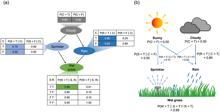 | ||
| Fig. 1 An example of a simple Bayesian network. (a) Bayesian network consisting of four nodes with conditional probability tables (CPTs). (b) Schematic of colored conditional probabilities in (a). Arrows represent the causal relationship between the nodes of the Bayesian network. | ||
P(Cloudy = T) is a prior probability, the probability of the weather being ‘Cloudy’ estimated from the long-term observed data.8 Also, P(Sprinkler = T|Cloudy = F) represents the likelihood, which can be determined by the observed conditional probability in the CPT data in Fig. 1a. Fig. 1b illustrates the causal relationship within the bayesian network in Fig. 1a, including the prior probabilities and likelihoods.
Bayesian inference refers to the computation of the posterior probability, which is unavailable in the CPT data.8 For instance, P(W = T) is the nodal probability not explicitly shown in the CPT. The marginalization based on Bayes' theorem must be conducted to infer this probability (ESI, Note S1†). P(W = T|C = T) is the hidden conditional probability signifying the causal relationship between ‘Wet grass’ and its grandparent node, ‘Cloudy’. In addition, P(R = T|W = T) is the inverse conditional probability characterizing the relationship between the cause and the result in an opposite manner. Bayesian inference enables finding the hidden and inverse conditional probabilities. Note S2 of the ESI† shows the Bayesian inference of the network displayed in Fig. 1a, where the Bayesian inference of P(R = T|W = T) requires extensive analytic computations, including a multiplication and marginalization process to convert probabilities into likelihoods. Therefore, calculation complexity increases exponentially as the node number in the Bayesian network increases. Specifically, the complexity of the analytic calculation in the Bayesian inference is O(2n) for the binary case, where ‘n’ is the number of nodes within the Bayesian network.9
In a general Bayesian network, many nodes may have multiple parent and child nodes, and multiple hops to ancestors and descendants may be present, where hop means the number of edges between the two nodes. For example, the Bayesian network of schizophrenia and mixed dementia diagnosis has 29 nodes, with several nodes having up to 5 parent nodes and 4 child nodes.10 In such cases, the arithmetic operations involved in Bayesian inference become computationally challenging with conventional complementary metal-oxide-semiconductor (CMOS) technology.11–13
Besides, the Bayesian inference requires random numbers to calculate the probability. In conventional CMOS technology, lookup tables, comparators, and linear feedback shift registers (LFSRs) have been used to generate random numbers. However, due to the deterministic characteristics of the CMOS hardware, for example, a thirty-two-stage LFSR was used to extract random numbers, which required ∼1200 transistors.14 The conventional CMOS-based algorithm also requires complex floating-point calculations, consuming excessive energy.15,16 All these factors render implementing the Bayesian inference in CMOS circuits challenging regarding area and power consumption.
On the other hand, due to their inherent stochastic properties, emerging memory devices, such as magnetic tunnel junctions (MTJs) and memristors, have been utilized as random number generators.17–21 The MTJ offers a robust operation but requires complex thin film material stacks, complicating its fabrication process. Also, its low on/off ratio (only 2∼3) causes errors during the output sensing, thus requiring additional amplifying circuits. In contrast, the memristor consists of a simple metal-insulator-metal (MIM) structure with an on/off ratio of several orders of magnitudes, negating the demerits of MTJ devices. However, its non-volatile memory switching requires repeated application of RESET (switching from the low resistance state (LRS) to the high resistance state (HRS)) voltages, which requires an additional voltage source and time step.22 In contrast, the threshold switching (TS) device, which switches to the HRS even without the RESET voltage application from the LRS after the SET (switching from the HRS to the LRS), can alleviate the problem, rendering it a suitable random source for Bayesian circuits.
This study suggested an efficient circuit for the Bayesian network and Bayesian inference using a Cu0.1Te0.9/HfO2/Pt (CTHP) diffusive memristor, exhibiting a TS behavior with an on/off ratio exceeding 104.23 A probabilistic-bit (p-bit) neuron capable of controlling spiking probability by varying the input voltage was demonstrated using this TS device. In the Bayesian network hardware, each p-bit neuron represents a node, and positive edge-triggered D flip-flops and a 2n × 1 multiplexer (MUX), where ‘n’ signifies the number of parent nodes, constitute the edges. The probability of each node being ‘True’ was derived through parallel sampling in the Bayesian network hardware using the p-bit neurons. Furthermore, Bayesian inference was implemented by calculating conditional probability through the intersection and division of sampled nodal probabilities using an additional peripheral p-bit neuron. A feedback procedure with an exponentially decreasing learning rate was incorporated to avoid the inherent memristor noise, enhancing the accuracy of the Bayesian inference even for complex Bayesian networks.
Results and discussion
Probabilistic and threshold switching behavior of a CTHP memristor
Fig. 2 shows the structure of the CTHP memristor. The CTHP memristor was fabricated in a cross-point configuration with an effective electrode area of 10 × 10 μm2, as shown in the scanning electron microscopy (SEM) image in Fig. 2a. The structure of the memristor was confirmed by a cross-section scanning transmission electron microscope (STEM) image and a line scan in energy-dispersive X-ray spectroscopy (EDS), as shown in Fig. 2b and c. The amorphous phase of HfO2 and crystal orientation of the active electrode within the CTHP memristor were confirmed by glancing angle X-ray diffraction, as shown in Fig. S1 of the ESI.† The CTHP memristor is a metal filamentary-type device where the switching occurs through the formation and rupture of Cu filaments, which originate from the CuxTe1−x active electrode.24 The process of on-switching consists of three steps: (1) ionization of the Cu into Cuz+ ions at the active electrode, (2) migration of Cuz+ ions through HfO2, and (3) nucleation (reduction) of Cuz+ ions into Cu at the Pt electrode.25 In the first step, there are two mechanisms for the ionization of the Cu at the Cu0.1Te0.9/HfO2 interface: (1) anodic dissolution of the Cu from the Cu0.1Te0.9 active electrode, and (2) extraction of Cuz+ ions from the CuOx at the Cu0.1Te0.9/HfO2 interface.26 CuOx can exist at the Cu/HfO2 interface due to the oxygen supply from HfO2.27 The electric field can break the chemical bonds in CuOx, separating the Cuz+ ions from the oxygen ions, and inject Cuz+ ions into the oxide.28–30 Among Cu2O and CuO, bond strength of CuO (Cu2+–O2) is 40% that of Cu2O (Cu+–O2−) due to the weak orbital hybridization.31 Moreover, Cu can be ionized preferentially to Cu2+ rather than Cu+ under the applied electric field.32 Therefore, Cu2+ ions become a dominant migration ion instead of Cu+. Fig. 2d shows the X-ray photoelectron spectroscopy (XPS) depth profiling analysis of the Cu 2p3/2 peaks (931.57 eV) in the CTHP memristor. The proportion of CuO 2p3/2 peaks (932.5 eV) increases as the data-acquiring surface approaches the Cu0.1Te0.9/HfO2 interface (at an etching time of 100 s). The XPS analysis results of Cu 2p1/2 indicate the same tendency, as shown in Fig. S2a of the ESI.† Additionally, XPS analysis of the Hf 4f peak in Fig. S2b of the ESI† shows that the binding energy of Hf has increased as it moves from the interface (100 s) to bulk (180 s). This proves that HfO2 at the interface is oxygen-deficient compared to bulk HfO2 because it supplied oxygen to Cu.33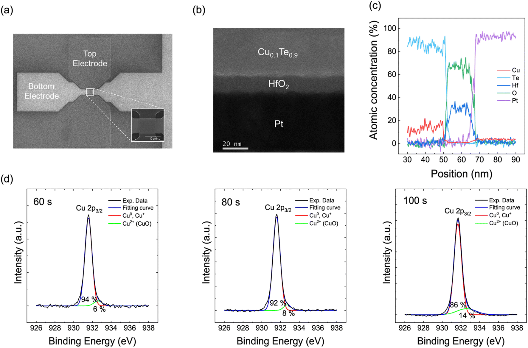 | ||
| Fig. 2 Structure analysis of the Cu0.1Te0.9/HfO2/Pt (CTHP) memristor. (a) Scanning electron microscope (SEM) image of the cross-point structure. The area of the cross point is 10 × 10 μm2. (b) Cross-section scanning transmission electron microscope (STEM) image of the CTHP memristor. (c) Depth profiles analyzed by energy-dispersive X-ray spectroscopy (EDS). (d) X-ray photoelectron spectroscopy (XPS) depth profiling analysis results for Cu 2p3/2 spectroscopy in the CTHP memristor. | ||
Cu-based filamentary switching memristors usually exhibit non-volatile behavior due to injecting a large amount of Cu ions into the oxide, forming thick Cu filaments.34 Conversely, the device shows volatile TS behavior when Cu and Te are co-sputtered with a sufficiently small atomic ratio of Cu (ca., Cu0.1Te0.9 as in this work). In this case, the number of Cu ions driven into the HfO2 film decreases, causing the filament size to fall below a threshold for stable filament formation.35 Consequently, the filament dissolves to reduce the interface energy between the Cu filaments and the HfO2 matrix when the voltage is removed, thus showing the TS behavior.
Fig. 3a shows 40 consecutive current–voltage (I–V) curves with a 10 nA compliance current. After the electroforming process occurred at 3.25 V during the first I–V sweep, the device showed a volatile switching with the threshold voltage between 1.5 V and 2.7 V. A sufficiently high voltage is required to ionize Cu atoms and nucleate at the Pt surface to form the first Cu filaments inside pristine HfO2. After electroforming, the effective thickness of the oxide decreases due to the residual Cu filament within the oxide, thus reducing the threshold voltage.26
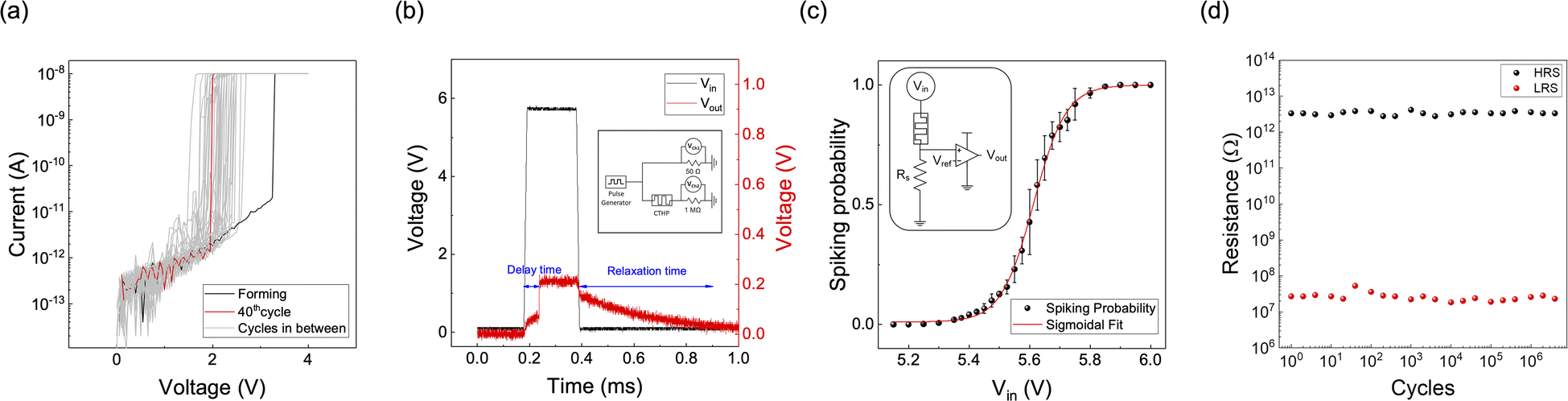 | ||
| Fig. 3 Electrical measurement of the CTHP memristor and p-bit neuron. (a) DC I–V curves of the CTHP memristor with 10 nA compliance current (Icc). (b) Threshold switching of the CTHP memristor by the pulse measurement. The input voltage, marked in black, is applied to the top electrode of the device. The output voltage from the device, marked in red, shows threshold switching behavior with delay and relaxation time. The inset shows a circuit configuration of the pulse measurement. VCh1 represents the input voltage from the pulse generator, and VCh2 represents the output voltage. (c) Spiking probability of the CTHP-based p-bit neuron as a function of Vin. Each probability is calculated from probability samples measured in 128 pulses. The inset shows a schematic of the CTHP-based p-bit (probabilistic-bit) neuron. It consists of a memristor, a series resistor (2.2 MΩ), and a comparator. (d) HRS and LRS resistance of the CTHP memristor during endurance tests under the same pulse length and cycle as in (c). | ||
The intrinsic stochasticity of the threshold voltage is derived from the random detachment of Cu nanoclusters from the active electrode (Cu0.1Te0.9). The device switches to an on-state by a positive voltage and spontaneously returns to an off-state upon voltage removal, exhibiting TS behavior. In contrast, Fig. S3 of the ESI† shows that the device with Cu0.2Te0.8 does not exhibit a stable TS behavior since the amount of Cu clusters remaining in the oxide increases during switching. Moreover, in the case of Cu0.3Te0.7, the set voltage shifts to the lower voltage region during the sequential DC sweeps, ultimately exhibiting non-volatile resistive switching (RS) behavior. As a result, the Cu0.1Te0.9 device that shows a stochastic TS behavior without memory was selected for the Bayesian network implementation.
The pulse operation further confirmed TS behavior of the Cu0.1Te0.9 device, as shown in Fig. 3b. With a 5.8 V input voltage (Vin), the CTHP memristor switches to the on-state after a delay of ∼70 μs. After the pulse termination, the CTHP memristor returns to its off-state with a relaxation time of ∼500 μs. These stochastic TS behaviors of the CTHP memristor could be adopted to compose a p-bit neuron, as discussed below.
A p-bit neuron circuit consisting of a CTHP memristor, a series resistor Rs (2.2 MΩ), and a comparator (HA17393, Renesas, Japan) is implemented, as shown in the inset of Fig. 3c. It is designed to output either Vdd (4.6 V in this work) or 0 V probabilistically, where the input voltage controls the probability. As the input voltage increases, the probability of the memristor becoming the on-state increases. Consequently, the input voltage applied to the comparator exceeds its reference voltage (Vref) of 0.3 V more frequently, thus showing a higher probability of output Vdd. Fig. S4 of the ESI† shows the p-bit outputs at three different input voltages (5.40 V, 5.60 V, and 5.80 V). For the p-bit generation, each cycle has a pulse length of 400 μs with 10 ns of leading and trailing times, and the pulse cycle was set to 4 ms. Fig. 3c shows the spiking probability of the p-bit neuron circuit based on the input voltage, and the average and standard deviation (SD) are calculated from 512 samples at each voltage point. The spiking probability in response to input pulses follows a sigmoidal relation, suitable for the Bayesian network. Fig. 3d shows the endurance of the CTHP-based p-bit neuron by showing the uniform HRS and LRS resistance during 4 × 10⁶ cycles under the same pulse length and cycle as in Fig. 3c. The p-bit neuron can operate for much more than 4 × 10⁶ cycles because the endurance test was conducted at a voltage of 7 V, which switches the CTHP memristor to 100% probability.
Hardware implementation of a Bayesian network
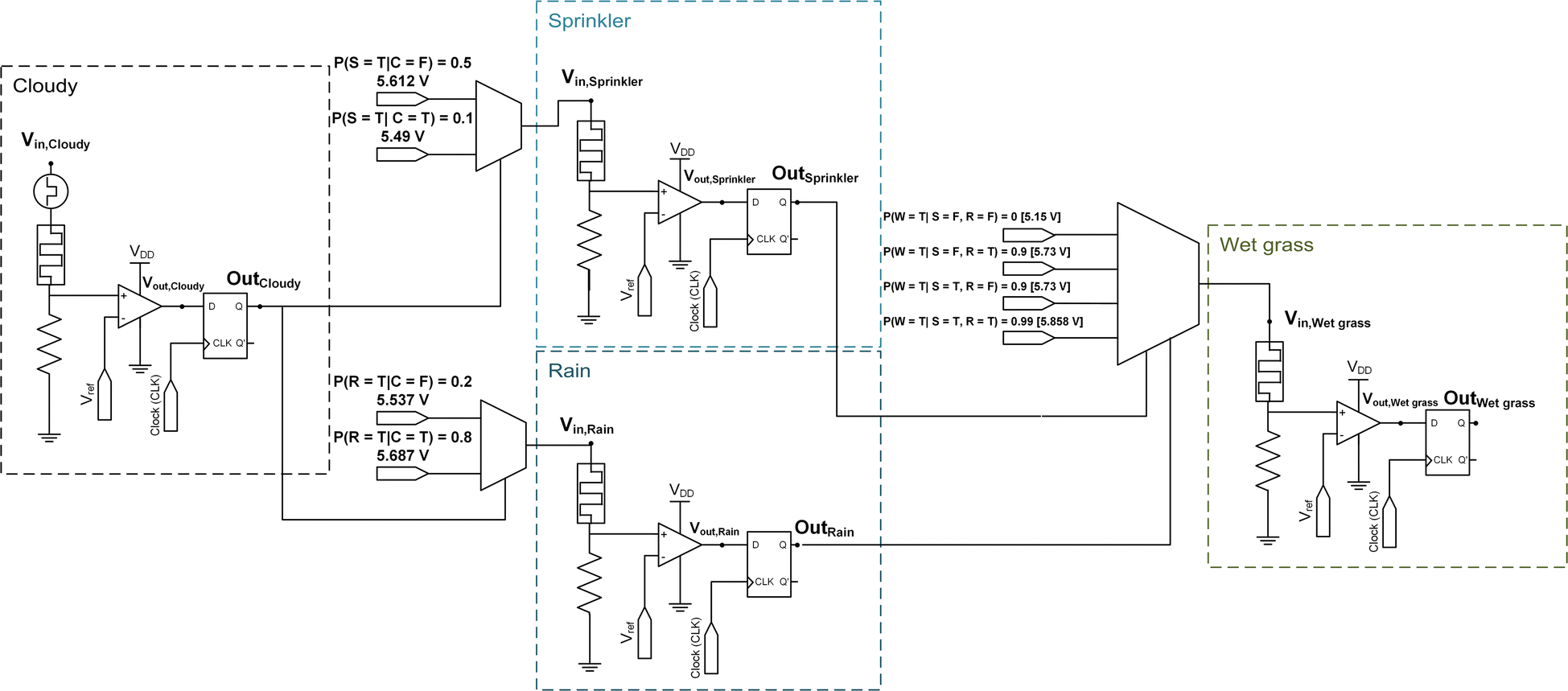
A Bayesian network was demonstrated using the CTHP-based p-bit neurons as nodes integrated with the CMOS-based edges, signifying conditional dependencies. In the following sections, Bayesian networks are simulated based on the experimental p-bit neuron data (see the Experimental Section) and simulated CMOS-based edges. Fig. 4a illustrates the interconnection circuit diagram between two nodes, the ‘Cloudy’ and the ‘Sprinkler’ shown in Fig. 1, where each node is composed of a p-bit neuron (composed of CTHP, a resistor, and a comparator) and a D-flip-flop. The two nodes are connected via a 2 × 1 MUX, where the voltages corresponding to P(S = T|C = F) = 0.5 (5.612 V) and P(S = T|C = T) = 0.1 (5.49 V) are selected as outputs, representing the part of the CPT of ‘Sprinkler’.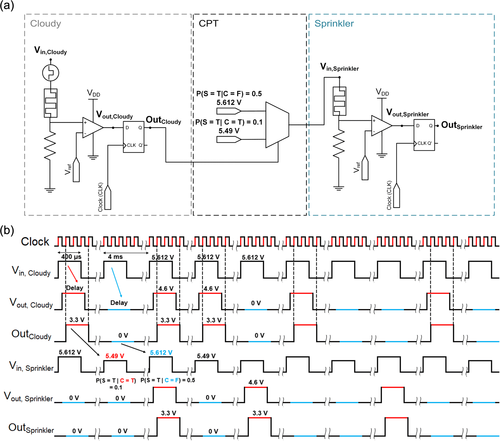 | ||
| Fig. 4 Working principle of the p-bit neuron-based Bayesian network. (a) Schematic of the interconnection between two nodes in a simple Bayesian network. Two nodes from Fig. 1a, ‘Cloudy’ and ‘Sprinkler,’ are represented as p-bit neurons in dashed boxes. The interconnection between the two nodes consists of a positive edge-triggered D flip-flop and a multiplexer (MUX). The MUX interconnects the two nodes by selecting the input voltage for the ‘Sprinkler’ node according to the output of the ‘Cloudy’ node. (b) The timing diagram for the circuit in (a). The output of the p-bit neuron, Vout, is generated probabilistically for each node according to the Vin. The delay between Vin and Vout is due to the delay time of the memristor. The D flip-flop samples the input (Vout, Cloudy) at every rising edge of the clock and updates the output (OutCloudy). | ||
First, an input pulse voltage of 5.612 V is applied to a p-bit neuron of the ‘Cloudy’ node. The probability that the neuron output produces Vout, Cloudy is 50%, thereby defining the value for Pprior(C = T). Then, Vout, Cloudy feeds into a D flip-flop that acts as a buffer memory, and the output of the D flip-flop (OutCloudy) enters into a MUX, which stores the CPT data in voltage values. Subsequent pulses are selected according to the binary states of parent nodes, and the amplitudes of the pulses are determined from the CPT.
Fig. 4b illustrates the timing diagram of the interconnection circuit between the ‘Cloudy’ and ‘Sprinkler’ nodes. Following the clock signal, Vin, Cloudy is applied to the input of the p-bit neuron of the ‘Cloudy’ node with a pulse length of 400 μs with a period of 4 ms (first row). Vout, Cloudy (=4.6 V) in response to Vin, Cloudy is generated from the p-bit neuron with the various delay times in each cycle marked as a red or a blue line (ground) when it is ‘1’ or ‘0’ (second row). OutCloudy (3.3 V pulse in this work) is updated with Vout, Cloudy values at the rising edge of the clock signal through the D flip-flop, which synchronizes the outputs of all nodes at each cycle (third row). The synchronization is necessary for multiple-parent cases with different delay times. After the 2 × 1 MUX receives OutCloudy as an input, it generates a voltage signal that defines the spiking probability of the ‘Sprinkler’ node. For instance, if OutCloudy is ‘1’ (i.e., 3.3 V) the MUX yields an output of 5.49 V (fourth row), corresponding to the 10% spiking probability of the ‘Sprinkler’ node. Therefore, for example, during the 100 sampling periods, ∼50 of OutCloudy is ‘1’. These 50 OutCloudy then induce ∼5 of OutSpringkler being ‘1’ (fifth and sixth rows) among the 50 operation cycles of the Sprinkler node. In this way, the Vin, Sprinkler encodes the conditional probability of P(S = T|C = T). For the remaining ∼50 cases of the OutCloudy being ‘0’, the MUX yields an output of 5.612 V (fourth row), which then induces ∼25 of OutSpringkler being ‘1’ during the remaining 50 operation cycles. In this case, the conditional probability refers to P(S = T|C = F). Consequently, the ‘Sprinkler’ node output, OutSprinkler, encodes the entire probability of P(S = T). As shown in Table 1, the theoretical value of P(S = T) is 0.3, which can be derived from the above experiment using P(S = T) = P(S = T|C = T) + P(S = T|C = F), where P(S = T|C = T) and P(S = T|C = F) values are 0.5 × 0.1 and 0.5 × 0.5, respectively. The CTHP memristor exhibits volatile TS behavior, eliminating the RESET process throughout these repeated sampling cycles.
| Nodal probability | Theoretical | Inference | Number of samples | |
|---|---|---|---|---|
| 100 | 1000 | |||
| P(C = T) | 0.5 | Mean | 0.499 | 0.500 |
| SD | 0.043 | 0.044 | ||
| P(S = T) | 0.3 | Mean | 0.308 | 0.301 |
| SD | 0.042 | 0.040 | ||
| P(R = T) | 0.5 | Mean | 0.498 | 0.501 |
| SD | 0.039 | 0.044 | ||
| P(W = T) | 0.647 | Mean | 0.653 | 0.647 |
| SD | 0.042 | 0.039 | ||
A similar circuit can represent the entire Bayesian network shown in Fig. 1. Fig. 5 shows the overall circuit diagram of the Bayesian network composed of four p-bits. The probability values between the nodes are encoded as the amplitudes of the voltage pulse of the MUX connecting the nodes. As the ‘Wet grass’ node has two parents, a 4 × 1 MUX receives synchronized OutSprinkler and OutRain pulse streams as inputs. Subsequently, Vin, Wet grass are selected from four voltage sources according to the binary states of OutSprinkler and OutRain. Therefore, P(C = T), P(S = T), P(R = T), and P(W = T) can be derived through parallel sampling of the respective node outputs. Here, parallel sampling indicates a simultaneous counting of Out signals of each node for a given Vin, Cloudy.
 | ||
| Fig. 5 Implementation of a simple Bayesian network. A schematic of the Bayesian network in Fig. 1a, consisting of four p-bit neuron circuits. Each node corresponds to a CTHP-based p-bit neuron circuit. | ||
Moreover, the sampling process (O(1)) replaces the analytical Bayesian inference (O(2n)) of P(S = T), P(R = T), and P(W = T), which are not explicitly provided in the CPT. Specifically, the analytical Bayesian inference of P(W = T) consists of probability marginalization regarding the CPT of the parent nodes. The calculation of the nodal probabilities is detailed in Note S1 of the ESI.†
Table 1 summarizes the inference results of individual probabilities obtained from 100 and 1000 samples for each node shown in Fig. 5. A single sampling result is achieved by counting the number of output spikes resulting from the 128 input pulses into each node. The inferred mean values of the probabilities show proximity to the theoretical values with the normalized mean square error (NMSE) of 1.05 × 10⁻⁴ for 100 samples and 1.61 × 10⁻⁶ for 1000 samples. The cycle-to-cycle variation of CTHP memristors may have resulted in deviations from the mean values. Still, their SD was only ∼0.04, suggesting the robustness of the suggested method to infer the nodal probabilities. Moreover, the device's cycle-to-cycle variation, which resulted in a sigmoid curve variation (Fig. 3), did not affect the inference accuracy significantly, as shown in Fig. S5 of the ESI.†
Bayesian inference
Besides the nodal probabilities, the inference of the posterior probabilities is crucial in the Bayesian networks. A division feedback logic was suggested in a previous study for the general inference of the posterior probabilities within a Bayesian network.36–38 However, the proposed method was inadequate to suppress the noise from the device and circuit. Therefore, this work suggests a modified division feedback logic to infer the posterior probability from the estimated nodal probabilities in Table 1. Fig. 6a shows the schematic diagram of the suggested circuit, composed of three p-bit neurons and two AND gates for the intersection calculation and a modified division feedback logic block for error and feedback calculation. The following section explains how it calculates the posterior probabilities.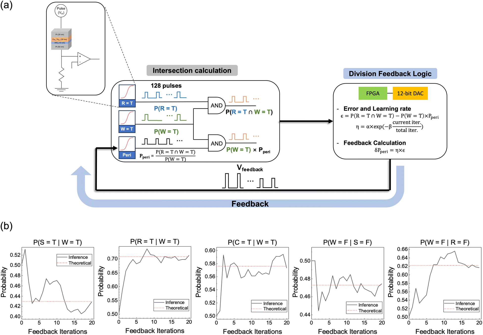 | ||
| Fig. 6 Division feedback logic and the inference results of the simple Bayesian network. (a) Schematic of a Bayesian inference circuit using division feedback logic and peripheral node. In the intersection calculation block, 128 pulses are sampled from three p-bit neurons, and intersection probabilities are calculated from AND gates. In the division feedback logic block, the difference between the two AND gate outputs is calculated as error ε and multiplied by the learning rate η through FPGA. Finally, the feedback voltage to the peripheral node is updated with the multiplied value, ε × η. Twenty feedback iterations are conducted for every inference, and the learning rate is updated for every iteration, as described in the equation. (b) The inference of five posterior probabilities through the division feedback logic. The inferred probability approaches the theoretical value according to the learning rate through the feedback iterations. | ||
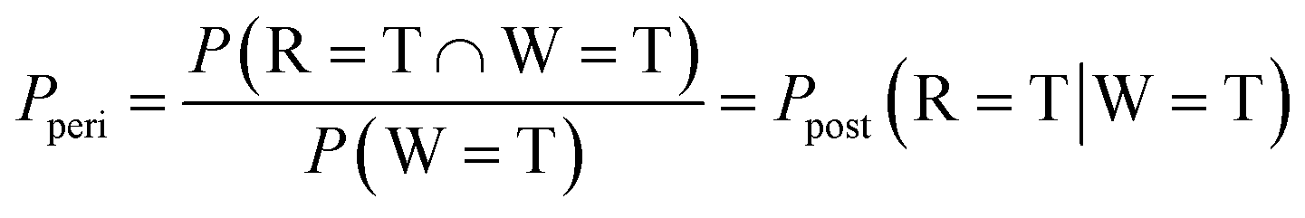
Suppose that, for example, Ppost (R = T|W = T) is sought, corresponding to the probability of raining when wet grass is observed, which is not a priori known from the given CPTs. This value can be found by a complicated theoretical mean, as shown in Note S2 of the ESI,† or through the inference using the suggested p-bit Bayesian circuit shown in Fig. 6. Ppost (R = T|W = T) can be expressed as P(R = T ∩ W = T)/P(W = T) by Bayes' theorem. An AND gate (upper AND gate in the left portion of Fig. 6a) efficiently implements P(R = T ∩ W = T) in the numerator by receiving pulses from two p-bit neurons as inputs (P(R = T) and P(W = T), which are reported in Table 1). In other words, the AND gate outputs a pulse only when the two inputs are simultaneously ‘1’. It should be noted that these two probability values have a conditional interrelationship.
On the other hand, dividing the P(R = T ∩ W = T) by P(W = T) requires additional circuit elements composed of an additional peripheral node and division feedback logic, as shown in Fig. 6a. The idea behind this suggested circuit is that the probability for the additional peripheral p-bit neuron (Peri node), Pperi, is assumed to correspond to the P(R = T ∩ W = T)/P(W = T) value. Thus, its value is taken as the solution to the problem when the inference error becomes sufficiently small. Then, the outputs of the ‘Wet grass’ and Peri nodes are input to another AND gate (lower AND gate in Fig. 6a), and the output of this AND gate corresponds to P(W = T) × Pperi because these two nodes are independent. Finally, the difference between the outputs of the two AND gates, defined as the error, ε, in the right portion of Fig. 6a, is estimated, which is then minimized by varying the input voltage to the Peri node. The ε minimization steps are described below.
The Pperi is initially set to 0.5 by inputting 5.612 V to this node. Then, after sampling 128 pulses from each node representing P(R = T), P(W = T), and Pperi, two AND gates output the intersection of the input p-bit pulses. For the probability calculation, the number of spiking pulses is divided by the total pulse number of 128.
Following the intersection calculation, the division feedback logic is utilized to infer the posterior probability using two output pulse streams from each AND gate. In the division feedback logic block shown in the right portion of Fig. 6a, Pperi is adjusted to equalize the number of spiking pulses from two AND gates. To perform this equalization, the difference between two probabilities, the ε, is calculated by using a field programmable gate array (the equation in the feedback logic block of Fig. 6a). Subsequently, the feedback voltage directed to the peripheral p-bit neuron is modified to minimize the ε. In this feedback stage, the ε is multiplied by the learning rate η, (η = α × exp(−β × current iter/total iter)) to determine the desired amount of change in the subsequent Pperi (δPperi). As a result, the feedback probability Pn+1 is equal to Pn + εn × ηn, where ‘n’ is the current number of feedbacks. The process of the probability feedback is described as follows.
| Pn+1 = Pn + εn × η | (1) |
Starting with P0 = 0.5, Pn+1 corresponds to the spiking probability of the peripheral node after the (n+1)th feedback. εn and ηn are the error and the learning rate at the (n+1)th feedback, respectively. Subsequently, the relationship between the feedback voltage and the spiking probability is shown as
| Pn+1 = f(Vn+1) | (2) |
The spiking probability in response to the feedback voltage after the (n+1)th feedback follows the sigmoidal function, as shown in Fig. 2f. Therefore, the (n+1)th feedback voltage is given by
| Vn+1 = f−1(Pn+1) | (3) |
The (n+1)th feedback voltage directed to the peripheral p-bit neuron is an inverse function of the sigmoidal function. During the feedback iteration, the learning rate (ηn) exponentially decreases as the ‘n’ increases, allowing for a gradual and incremental feedback mechanism. After twenty feedback iterations (Pperi = P20), the ε is minimized, and finally,
| P(R = T ∩ W = T) ≈ P(W = T) × Pperi | (4) |
 | (5) |
Fig. 6b shows the feedback results for five posterior probabilities of the network in Fig. 1a. The Pperi rapidly approaches the target value in the early iterations due to the high η. In contrast, in the later iterations, the feedback is depressed, preventing deviation from the target value. This process is similar to the simulated annealing method in the p-bit network.39 Throughout the inference, the feedback iterations and pulse numbers were chosen as 20 and 128, respectively. These values were selected considering the tradeoff between the calculation overhead and accuracy, detailed in Fig. S6 of the ESI.†
Table 2 summarizes the inference results of the five posterior probabilities. Meanwhile, the p-bit neuron outputs were inverted using a NOT gate for the probability of the nodes being ‘False.’ The mean values of all the posterior probabilities in the Bayesian network are precisely inferred with a low NMSE of 6.58 × 10⁻⁴ and 6.91 × 10⁻⁴ for 100 and 1000 samples, indicating that the division feedback logic feasibly infers the correct answers even within 100 samples. The SD values are also low (∼0.02) for 100 and 1000 samples, suggesting that the influence of the device variation is minimal. Further details regarding the variance tolerance of the proposed method are provided in Fig. S7 and 8 of the ESI.†
| Nodal probability | Theoretical | Inference | Number of samples | |
|---|---|---|---|---|
| 100 | 1000 | |||
| P post(S = T|W = T) | 0.430 | Mean | 0.427 | 0.430 |
| SD | 0.020 | 0.022 | ||
| P post(R = T|W = T) | 0.708 | Mean | 0.711 | 0.707 |
| SD | 0.022 | 0.019 | ||
| P post(C = T|W = T) | 0.576 | Mean | 0.578 | 0.575 |
| SD | 0.022 | 0.021 | ||
| P post(W = F|S = F) | 0.473 | Mean | 0.474 | 0.472 |
| SD | 0.022 | 0.022 | ||
| Ppost(W = F|R = F) | 0.622 | Mean | 0.619 | 0.619 |
| SD | 0.023 | 0.021 | ||
Finally, the high potential of the suggested method for inferencing in a complex Bayesian network was examined using the Bayesian network with 20 nodes and 7 layers, where the CPTs between the nodes are randomly generated, as shown in Fig. 7a. Fig. 7b shows the hardware implementation method for node 4 in the network, where an 8 × 1 MUX is utilized to encode the CPT from three parents (nodes 3, 16, and 17).
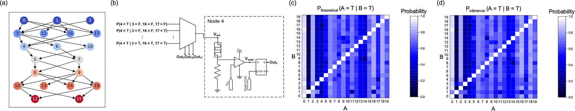 | ||
| Fig. 7 Inference of the complex Bayesian network. (a) A complex Bayesian network consisting of 20 nodes and 7 layers. (b) Partial hardware implementation scheme of node 4. Three parent nodes of node 4 and their probabilities are interconnected with an 8-to-1 MUX. (c) Colormap for the theoretical values of all conditional probabilities, P(A = T|B = T). (d) Colormap for the mean of the inference results of all conditional probabilities, P(A = T|B = T). Inference results consist of 100 samples for every posterior probability. | ||
The inference results of the suggested method are shown in Fig. 7c and d. Fig. 7c provides an overview of the theoretical posterior probability values across the entire network, calculated by a method similar to that in Note S2 of the ESI.† At the same time, Fig. 7d illustrates the inference outcomes of the posterior probabilities using the suggested Bayesian network circuit. The theoretical and inference values show 380 posterior probabilities, except for 20 posterior probabilities of the nodes conditioned on themselves (colored as white squares in Fig. 7c and d). The inference results in Fig. 7d show the mean value of 100 inferences for each posterior probability. The inference results match well with the theoretical results, implying that the suggested method can be used to analyze complex networks, such as autonomous vehicles, medical diagnosis, and forecasting.40–42
Table 3 shows five instances of inference outcomes for two inference samples (100 and 1000). The condition and result nodes are significantly distant in most of these conditional probabilities. For example, six hops are required between nodes 1 and 15. Nevertheless, the SD value is within 0.02 for most probabilities. This capacity for precise inference is further demonstrated by the low SD values (<0.03) of all the inference results, even in the 100 samples, as presented in Fig. S9 of the ESI.† The NMSE of all the mean inference probabilities in this complex Bayesian network is 3.37 × 10⁻³ for 100 and 1000 samples. It demonstrates accurate inferences with suppressed noise with only 100 samples, even in a complex Bayesian network.
| Nodal probability | Theoretical | Inference | Number of samples | |
|---|---|---|---|---|
| 100 | 1000 | |||
| P post(19 = T|0 = T) | 0.660 | Mean | 0.658 | 0.660 |
| SD | 0.020 | 0.020 | ||
| P post(2 = T|10 = T) | 0.820 | Mean | 0.811 | 0.814 |
| SD | 0.019 | 0.017 | ||
| P post(1 = T|15 = T) | 0.130 | Mean | 0.133 | 0.133 |
| SD | 0.020 | 0.015 | ||
| P post(15 = F|1 = F) | 0.331 | Mean | 0.333 | 0.331 |
| SD | 0.020 | 0.020 | ||
| P post(13 = F|10 = F) | 0.515 | Mean | 0.514 | 0.513 |
| SD | 0.023 | 0.022 | ||
In contrast to the analytical approach, which suffers from an exponential increase in computational resources with the increasing number of nodes, the proposed method achieves accurate inference of posterior probabilities by utilizing a constant number of pulses and feedback iterations. Further details regarding the inference and feedback are described in Fig. S10 of the ESI.†
Table 4 summarizes the comparison between different Bayesian inference circuits using various devices. A simple device structure, a high on/off ratio, and volatility of the CTHP memristor decreased the required number of transistors in a CTHP-based p-bit circuit compared to that in the previous studies.11,14,38,43 Remarkably, the power consumption per random neuron output of a CTHP p-bit neuron was significantly lower than that of CMOS-based LFSRs. The lower power consumption of the CTHP p-bit neuron is attributed to replacing random bit generation in a conventional LFSR with the inherently stochastic CTHP TS device. The CTHP p-bit neuron could be operated with a maximum power consumption of 186 nW, details of which estimation are included in the Experimental section below and Fig. S11 of the ESI.† Moreover, the CTHP p-bit neuron with a low current level generates random bits with lower power than those in previous studies of MTJ- and SiOx nanorod-based circuits, where an additional reset scheme or an extensive pulse width for the probability representation was further required.38,43 The detailed breakdown and calculation of the energy consumption in the suggested CTHP p-bit neuron are included in Table S1 and Note S3 of the ESI.†,44 For the accuracy of the Bayesian inference, the inference circuit based on the CTHP p-bit neuron achieved a lower NMSE in the inference of the network of four nodes than that of the network with similar sizes (∼ five nodes) based on the MTJ- and SiOx nanorod-based circuit.38,43 Furthermore, the inference for a more complex Bayesian network consisting of 20 nodes showed a comparable NMSE (3.37 × 10⁻³) to that in the other studies with simpler (∼ five nodes) networks.
| CMOS11,14 | MTJ43 | SiOx nanorods38 | This work | |
|---|---|---|---|---|
| Device structure | Complex | Complex | Simple MIM | Simple MIM |
| On/off ratio | — | 2∼3 | 104∼105 | 104 |
| Device volatility | Volatile | Non-volatile | Non-volatile | Volatile |
| Number of transistors | >1200 | >35 | 10 | 10 |
| Power consumption | 33.06 mW | 158.9 μW | 4.06 μW | <186 nW |
| Energy | 275.6 μJ | 692.4 fJ | 1.767 pJ | 441.4 fJ |
| Accuracy (NMSE) | — | 1.24 × 10⁻³ | 2.41 × 10⁻² | 7.5 × 10⁻⁴ |
Experimental section
Fabrication of the Cu0.1Te0.9/HfO2/Pt (CTHP) memristor
The cross-point structure of the Cu0.1Te0.9/HfO2/Pt (CTHP) memristor was fabricated on a SiO2/Si substrate. A 10 nm-thick Ti adhesion layer and a 50 nm-thick Pt bottom electrode were sequentially sputtered using a direct current (DC) sputtering system (MHS-1500, Muhan Vacuum Co). The bottom electrodes were patterned by photolithography, followed by a lift-off process. A 10 nm-thick HfO2 film was deposited on the bottom electrode using atomic layer deposition (ALD) at a 280 °C substrate temperature using a traveling-wave-type ALD reactor (Plus 200, CN-1 Co). Tetrakis dimethylamino hafnium (Hf[N(CH3)2]4) and O3 were used as precursors for Hf and reactive oxygen sources, respectively. A 30 nm-thick Cu0.1Te0.9 active electrode was co-sputtered on the HfO2 film by DC sputtering with a power of 10 W using a Cu target and radio frequency sputtering with a power of 120 W using a Te target (07SN014, SNTEK) at 4 mTorr pressure in Ar gas ambient at room temperature. A 30 nm-thick Pt capping layer was deposited on the active electrode using an electron beam evaporator (SRN-200, SORONA). Active electrodes and the capping layer were patterned by photolithography, followed by a lift-off process.Memristor structure analysis
A cross-point structure and a cross-sectional image of the CTHP memristor were acquired using SEM (S-4800, Hitachi) and STEM (JEM-ARM200F, JEOL), respectively. The chemical composition was analyzed using an EDS installed onto the STEM. The crystal orientation of electrodes and crystallinity of HfO2 were investigated via a glancing angle incidence X-ray diffractometer (PANalytical, X'Pert Pro MPD). The chemical analysis of the interfacial layer was conducted using XPS (AXIS SUPRA) with the Ar+ sputtering method.Electrical characterization
The I–V characteristics of the DC sweep mode were measured using a semiconductor parameter analyzer (HP4155A, Hewlett-Packard). The pulse measurement of alternating current (AC) mode was performed using a pulse generator (81110A, Agilent) and an oscilloscope (TDS 684C, Tektronix). The top electrode was biased, and the bottom electrode was grounded during the measurement.Normalized mean square error
The NMSE value was obtained by dividing the mean squared error of the inference result by the mean of the squared inference values.Power consumption calculation
The power consumption of a p-bit neuron was estimated using a resistance of the CTHP (RCTHP), a resistance of a serial resistor (RS), an input voltage (Vin), and a divided voltage (Vnode) between the CTHP and a serial resistor as shown in the inset of Fig. S7a of the ESI.† The power consumption of a serial resistor (PS) is presented as a function of RS and Vnode (eqn (6)), where Vnode is equal to VS.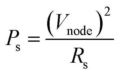 | (6) |
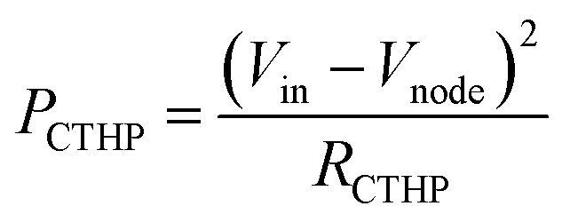
The power consumption of the CTHP (PCTHP) is described by a function of Vin, Vnode, and RS (eqn (7)), where (Vin − Vnode) is equal to VCTHP.
 | (7) |
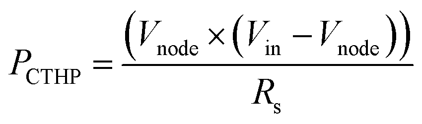
Kirchhoff's voltage law shows that the RCTHP can be represented as RS × (Vin − Vnode)/Vnode. Therefore, PCTHP could be presented as eqn (8).
 | (8) |
As a result, the total power consumption is given as eqn (9).
 | (9) |
Bayesian network simulation
The Bayesian networks and Bayesian inference were conducted based on the measurement data of the CTHP device. The overall simulation was based on Python, considering the device characteristics and inherent noise. Furthermore, the simulation of the feedback network, error calculation, and learning rate computations were executed using Python, following a similar methodology to that employed for device modeling.Conclusions
The Bayesian network was constructed utilizing CTHP-based p-bit neurons representing probabilities through the stochastic TS behavior. Bayesian inference was efficiently demonstrated within the Bayesian network, incorporating a feedback loop and an exponentially decaying learning rate. Notably, sampled probabilities from the individual node exhibited a low NMSE (∼10−4) and SD (∼0.04). In addition, the NMSE and SDs for all inference results within the complex network consisting of 20 nodes remained below 0.004 and 0.03, respectively, confirming the feasible mitigation of inherent memristor variations. Furthermore, the simple circuit design produced a low power consumption of 186 nW per p-bit neuron. Consequently, a single node within a Bayesian network was implemented with a low energy consumption of 441.4 fJ, outperforming the previous implementations. The suggested method can replace analytical probability calculations, which exponentially increase with the number of nodes (O(2n)) with a sampling and feedback mechanism (O(1)), thus enhancing computational efficiency.Author contributions
In Kyung Baek: conceptualization, methodology, writing – original draft, and writing – review and editing. Soo Hyung Lee: conceptualization, methodology, writing – original draft, and writing – review and editing. Yoon Ho Jang, Hyungjun Park, Jaehyun Kim, Sunwoo Cheong, Sung Keun Shim, Janguk Han, Joon-Kyu Han, Gwang Sik Jeon, and Dong Hoon Shin: methodology. Kyung Seok Woo: conceptualization, methodology, writing – original draft, writing – review and editing, and supervision. Cheol Seong Hwang: conceptualization, methodology, writing – original draft, writing – review and editing, and supervision.Conflicts of interest
The authors declare they have no conflict of interest.Acknowledgements
This work was supported by the National Research Foundation of Korea (No. 2020R1A3B2079882).Notes and references
- J. Pearl, Probabilistic Reasoning in Intelligent Systems: Networks of Plausible Inference, Morgan Kaufmann Publishers, San Mateo, Calif, 1988 Search PubMed.
- T. Tian, F. Kong, R. Yang, X. Long, L. Chen, M. Li, Q. Li, Y. Hao, Y. He, Y. Zhang, R. Li, Y. Wang and J. Qiao, Reprod. Biol. Endocrinol., 2023, 21, 8, DOI:10.1186/s12958-023-01065-x.
- V. X. C. Del Rosario, V. J. Narca, F. T. J. Laconsay and C. J. Alliac, in Proceedings – 2021 1st International Conference in Information and Computing Research, iCORE 2021, 2021 Search PubMed.
- C. Ottonello, M. Peri, C. Regazzoni and A. Tesei, in Conference Proceedings – IEEE International Conference on Systems, Man and Cybernetics, 1992 Search PubMed.
- C. Chen, D. Zhang, T. R. Hazbun and M. Zhang, Sci. Rep., 2019, 9, 1197, DOI:10.1038/s41598-018-37667-4.
- D. Heckerman and J. S. Breese, IEEE Trans. Syst. Man Cybern. A Syst. Hum., 1996, 26, 826–831, DOI:10.1109/3468.541341.
- T. Hujer, in Efficient Decision Support Systems - Practice and Challenges From Current to Future, 2011 Search PubMed.
- R. van de Schoot, S. Depaoli, R. King, B. Kramer, K. Märtens, M. G. Tadesse, M. Vannucci, A. Gelman, D. Veen, J. Willemsen and C. Yau, Nat. Rev. Methods Primers, 2021, 1, 1–26 CrossRef CAS.
- I. Ben-Gal, Bayesian Networks Encyclopedia of Statistics in Quality and Reliability, 2008 Search PubMed.
- D. I. Curiac, G. Vasile, O. Banias, C. Volosencu and A. Albu, in Proceedings of the International Conference on Information Technology Interfaces, ITI, 2009 Search PubMed.
- J. Kaiser and S. Datta, Appl. Phys. Lett., 2021, 119, 150503 CrossRef CAS.
- P. Mroszczyk and P. Dudek, in Proceedings - IEEE International Symposium on Circuits and Systems, 2014 Search PubMed.
- O. U. Khan and D. D. Wentzloff, IEEE Trans Very Large Scale Integr. VLSI Syst., 2015, 24, 837–845, DOI:10.1109/TVLSI.2015.2420663.
- W. A. Borders, A. Z. Pervaiz, S. Fukami, K. Y. Camsari, H. Ohno and S. Datta, Nature, 2019, 573, 390–393, DOI:10.1038/s41586-019-1557-9.
- L. Bagheriye and J. Kwisthout, Front. Neurosci., 2021, 15, 728086 CrossRef.
- M. Lin, I. Lebedev and J. Wawrzynek, in ACM/SIGDA International Symposium on Field Programmable Gate Arrays - FPGA, 2010 Search PubMed.
- K. Y. Camsari, P. Debashis, V. Ostwal, A. Z. Pervaiz, T. Shen, Z. Chen, S. Datta and J. Appenzeller, Proceedings of the IEEE, 2020, 108, 1322–1337, DOI:10.1109/JPROC.2020.2966925.
- H. Aziza, J. Postel-Pellerin, H. Bazzi, P. Canet, M. Moreau, V. Della Marca and A. Harb, IEEE Trans. Nanotechnol., 2020, 19, 214–222, DOI:10.1109/TNANO.2020.2976735.
- R. Faria, J. Kaiser, K. Y. Camsari and S. Datta, Front. Comput. Neurosci., 2021, 15, 584797, DOI:10.3389/fncom.2021.584797.
- P. Debashis, V. Ostwal, R. Faria, S. Datta, J. Appenzeller and Z. Chen, Sci. Rep., 2020, 10, 16002, DOI:10.1038/s41598-020-72842-6.
- K. Y. Camsari, S. Salahuddin and S. Datta, IEEE Electron Device Lett., 2017, 38, 1767–1770, DOI:10.1109/LED.2017.2768321.
- K. E. Harabi, T. Hirtzlin, C. Turck, E. Vianello, R. Laurent, J. Droulez, P. Bessière, J. M. Portal, M. Bocquet and D. Querlioz, Nat. Electron., 2023, 6, 52–63, DOI:10.1038/s41928-022-00886-9.
- K. S. Woo, J. Kim, J. Han, W. Kim, Y. H. Jang and C. S. Hwang, Nat. Commun., 2022, 13, 5762, DOI:10.1038/s41467-022-33455-x.
- K. S. Woo, J. Kim, J. Han, J. M. Choi, W. Kim and C. S. Hwang, Adv. Intell. Syst., 2021, 3, 2100062, DOI:10.1002/aisy.202100062.
- R. Waser, R. Dittmann, C. Staikov and K. Szot, Adv. Mater., 2009, 21, 2632–2663 CrossRef CAS.
- T. Tsuruoka, K. Terabe, T. Hasegawa, I. Valov, R. Waser and M. Aono, Adv. Funct. Mater., 2012, 22, 70–77, DOI:10.1002/adfm.201101846.
- J. Yang, H. Ryu and S. Kim, Chaos, Solitons Fractals, 2021, 145, 110783, DOI:10.1016/j.chaos.2021.110783.
- B. G. Willis and D. V. Lang, Thin Solid Films, 2004, 467, 284–293, DOI:10.1016/j.tsf.2004.04.028.
- L. P. Shepherd, A. Mathew, B. E. McCandless and B. G. Willis, J. Vac. Sci. Technol., B: Microelectron. Nanometer Struct.–Process., Meas., Phenom., 2006, 24, 1297–1302, DOI:10.1116/1.2200372.
- I. Valov, ChemElectroChem, 2014, 1, 26–36 CrossRef.
- D. Y. Cho, S. Tappertzhofen, R. Waser and I. Valov, Nanoscale, 2013, 5, 1781–1784, 10.1039/c3nr34148h.
- T. Tsuruoka, I. Valov, S. Tappertzhofen, J. Van Den Hurk, T. Hasegawa, R. Waser and M. Aono, Adv. Funct. Mater., 2015, 25, 6374–6381, DOI:10.1002/adfm.201500853.
- R. Jiang, X. Du, Z. Han and W. Sun, Appl. Phys. Lett., 2015, 106, 173509, DOI:10.1063/1.4919567.
- H. J. Kim, J. Kim, T. G. Park, J. H. Yoon and C. S. Hwang, Adv. Electron. Mater., 2022, 8, 2100209, DOI:10.1002/aelm.202100209.
- L. Goux, K. Opsomer, R. Degraeve, R. Mller, C. Detavernier, D. J. Wouters, M. Jurczak, L. Altimime and J. A. Kittl, Appl. Phys. Lett., 2011, 99, 53502, DOI:10.1063/1.3621835.
- C. S. Thakur, S. Afshar, R. M. Wang, T. J. Hamilton, J. Tapson and A. van Schaik, Front. Neurosci., 2016, 10, 104, DOI:10.3389/fnins.2016.00104.
- Y. Shim, S. Chen, A. Sengupta and K. Roy, Sci. Rep., 2017, 7, 14101, DOI:10.1038/s41598-017-14240-z.
- S. Choi, G. S. Kim, J. Yang, H. Cho, C. Y. Kang and G. Wang, Adv. Mater., 2022, 34, 2104598, DOI:10.1002/adma.202104598.
- N. A. Aadit, A. Grimaldi, M. Carpentieri, L. Theogarajan, J. M. Martinis, G. Finocchio and K. Y. Camsari, Nat. Electron., 2022, 5, 460–468, DOI:10.1038/s41928-022-00774-2.
- C. Dezan, S. Zermani and C. Hireche, Algorithms, 2020, 13, 155, DOI:10.3390/A13070155.
- R. Collins and N. Fenton, medRxiv Search PubMed.
- B. Abramson, J. Brown, W. Edwards, A. Murphy and R. L. Winkler, Int. J. Forecast., 1996, 12, 57–71, DOI:10.1016/0169-2070(95)00664-8.
- X. Jia, J. Yang, Z. Wang, Y. Chen, H. H. Li and W. Zhao, in Proceedings of the Asia and South Pacific Design Automation Conference, ASP-DAC, 2018 Search PubMed.
- S. in Yi, J. D. Kendall, R. S. Williams and S. Kumar, Nat. Electron., 2023, 6, 45–51, DOI:10.1038/s41928-022-00869-w.
Footnotes |
| † Electronic supplementary information (ESI) available. See DOI: https://doi.org/10.1039/d3na01166f |
| ‡ These authors contributed equally. |
| This journal is © The Royal Society of Chemistry 2024 |