
 Open Access Article
 This Open Access Article is licensed under a Creative Commons Attribution-Non Commercial 3.0 Unported Licence
Precise synthesis of copper selenide nanowires with tailored Cu vacancies through photo-induced reduction for thermoelectric applications†
Shunya
Sakane
 *a,
Tatsuki
Miura
b,
Kazuki
Munakata
b,
Yusuke
Morikawa
b,
Shunichiro
Miwa
b,
Riku
Yamanaka
c,
Toshiki
Sugai
c,
Akito
Ayukawa
a,
Haruhiko
Udono
a and
Hideki
Tanaka
*b
*a,
Tatsuki
Miura
b,
Kazuki
Munakata
b,
Yusuke
Morikawa
b,
Shunichiro
Miwa
b,
Riku
Yamanaka
c,
Toshiki
Sugai
c,
Akito
Ayukawa
a,
Haruhiko
Udono
a and
Hideki
Tanaka
*b
aGraduate School of Science and Engineering, Ibaraki University, 4-12-1, Nakanarusawa-cho, Hitachi, Ibaraki 316-8511, Japan. E-mail: shunya.sakane.sz12@vc.ibaraki.ac.jp
bFaculty of Science and Engineering, Chuo University, 1-13-27, Kasuga, Bunkyo-ku, Tokyo, 112-8551, Japan. E-mail: htanaka@kc.chuo-u.ac.jp
cFaculty of Science, Toho University, 2-2-1, Miyama, Funabashi-shi, Chiba 274-8510, Japan
First published on 24th April 2024
Abstract
Nanostructuring in α-Cu2Se while optimizing carrier concentration holds the promise of realizing further high thermoelectric performance at near room temperature. Nevertheless, controlling the amounts of Cu vacancies, which work as acceptors, in nanostructures is considerably more intricate than in bulk materials. Hence, controlling the amounts of Cu vacancies while maintaining the α-phase and nanostructure shape poses a formidable challenge. In this study, we synthesized Cu2+xSe nanowires (NWs) with various amounts of Cu vacancies at room temperature by the photoreduction method and investigated their thermoelectric properties. Cu2+xSe NWs exhibited a comparable thermoelectric power factor to that of the polycrystalline films fabricated at higher temperature. The achievement of the high power factor despite low-temperature fabrication is attributed to the precise synthesis of Cu2+xSe NWs with various amounts of Cu vacancies. We also investigated the reaction process of Cu2.00Se NWs in detail by observing the reaction intermediates. It was found that photoreduction occurred with Cu2+ ions adsorbed on Se NWs, leading to the reaction of Cu2+ ions and Se NWs without Cu deficiency. Namely, this photoreduction under the adsorbed conditions realized the control of Cu vacancies in Cu2+xSe NWs.
Introduction
Thermoelectric conversion is one of the energy harvesting techniques. The efficiency monotonically increases with the thermoelectric figure of merit ZT (=S2σT/κ), where S is the Seebeck coefficient, σ is the electrical conductivity, κ is the thermal conductivity, and T is the absolute temperature. To maximize thermoelectric performance of the material, it is effective to optimize carrier concentration and introduce nanostructures,1–21 which can control phonon and carrier transport.Cu2Se22–31 is a promising thermoelectric material because it exhibits a high ZT of 0.68 at near room temperature (RT).22 Therein, the carrier concentration is optimized to maximize the thermoelectric power factor (S2σ) by controlling the amounts of Cu vacancies, which work as acceptors. Nanostructuring while optimizing the carrier concentration holds the promise of realizing a higher thermoelectric performance. Nevertheless, controlling the amounts of Cu vacancies in nanostructures is considerably more intricate than in bulk materials. When the amounts of Cu vacancies increase excessively in the nanostructures, they easily distort the structures of the α-phase (semiconductor phase) until the rearrangement of the β-phase (metallic phase) is energetically favorable due to the larger contribution of the surface energy to the total energy of formation than that of bulk.32 Hence, controlling the amounts of Cu vacancies while maintaining the α-phase and nanostructure shape poses a formidable challenge. Furthermore, it is important to achieve high thermoelectric performance by controlling Cu vacancies with low-temperature synthesis to get practical advantages in applications such as flexible substrates with low heat resistance.
Recently, we developed the synthesis of single-phase α-Cu2Se nanowires (NWs) through the photoreduction method. Our group synthesized size-controlled Cu nanoparticles by the photoreduction method,33–39 where the slow reaction can control the morphology of copper nanoparticles.35 We applied the above method to the synthesis of α-Cu2Se NWs. Furthermore, we demonstrated S2σ enhancement of poly (3,4-ethylenedioxythiophene): poly (styrene sulfonate) (PEDOT:PSS) by introduction of Cu2Se NWs.40
In this study, we synthesized Cu2+xSe NWs with various amounts of Cu vacancies by the photoreduction method at RT and systematically investigated their thermoelectric properties. The thermoelectric properties were discussed in relation to Cu vacancies, which largely affect S2σ. Furthermore, we elucidated the impact of the deliberately slow reduction process on achieving the precise synthesis of Cu2+xSe NWs with various amounts of Cu vacancies by analyzing the reaction intermediates and providing a detailed discussion on the reaction kinetics.
Experimental
Synthesis of Cu2+xSe NWs
Se NWs were synthesized by the following method.41 SeO2 (25 mg, FUJIFILM Wako Pure Chemical Corporation) and β-cyclodextrin (50 mg, FUJIFILM Wako Pure Chemical Corporation) were dissolved in 10 mL of Milli Q water and stirred under ultrasonication for 10 min. The solution was slowly added into L-ascorbic acid solution prepared with L-ascorbic acid (0.2000 g, Wako Pure Chemical Corporation) and Milli-Q water (10 mL) and was stirred for 4 hours. The mixed solution was centrifuged, and the resulting precipitates were washed with ethanol and Milli-Q water several times alternately. The precipitates were redispersed in ethanol without stirring for >4 hours, forming Se NWs as precipitates.The synthesis method of Cu2Se NWs is shown below. The Se NWs (10 mg) were dispersed in copper acetate solution prepared by dissolving 253 μmol of copper acetate in aqueous solution containing 1 mL ethanol. The total volume of the dispersion thus obtained was adjusted to 10 mL by using Milli-Q water. The adjusted dispersion was irradiated using UV light (Hamamatsu Photonics: L9588-01A) with stirring for 12 hours, and Cu2Se NWs were obtained as precipitates. The Cu2+xSe NWs were also synthesized with some composition ratios (x = −0.05–0.20) by varying the amounts of copper acetate solution. To elucidate the reaction mechanism of Cu2Se NWs through the photoreduction method, Cu2Se NWs were also synthesized using UV light irradiation for 0–12 hours.
Structural characterization of Cu2+xSe NWs
The crystal structures of the Cu2+xSe NWs were characterized by powder X-ray diffraction (XRD) with an X-ray diffractometer (Rigaku, Smartlab), scanning electron microscopy (SEM)-energy dispersive X-ray spectroscopy (EDX) with a field-emission SEM (Hitachi High-Technologies, S-5500), and high-resolution transmission electron microscopy (HRTEM) with a TEM (Thermo Fisher Scientific, Tecnai G2 F20 S-TWIN, FEI). The composition ratios of Cu2+xSe NWs were quantified by EDX, where the quantified excessive Cu amounts are defined to be xq in this paper. The NW powders were also characterized by diffuse reflectance (DR) UV-vis spectrometry with a UV vis-NIR spectrometer (Shimadzu, UV-3600). The DR UV-vis-NIR spectra were obtained by using the Kubelka–Munk function F(R) to convert diffuse reflectance into an equivalent absorption coefficient, as follows: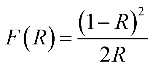 | (1) |
Evaluation of thermoelectric properties of Cu2+xNWs
The synthesized Cu2+xSe NW powders were pressed at 160 MPa for 1 min to form Cu2+xSe NW films at RT for the measurement of thermoelectric properties. The NW structures were maintained even after pressing (Fig. S1†). S was measured by using a ZEM-3 (ADVANCE RIKO) and σ was measured by the van der Pauw method at RT. Carrier concentration and carrier mobility were measured by Hall effect measurement (TOYO Corporation, M91-RTMG05).Results and discussion
Fig. 1a shows the SEM image for the obtained copper selenide NWs. The NW structures were observed and the diameter and length of the NWs were 300 ± 100 nm and 10 ± 5 μm, respectively (Fig. S2†). Since these values were almost the same as those of the Se NWs,40 it is considered that copper selenide was formed directly on the Se NWs by photoreduction. Fig. 1b shows the HRTEM image of the NWs. The lattice spacings of monoclinic α-Cu2Se (400) and (090) were observed, which correspond to the circles in the fast Fourier transformation (FFT) image (Fig. 1c). Analysis results of various regions of NWs indicate that the obtained NWs were composed of polycrystalline α-Cu2Se.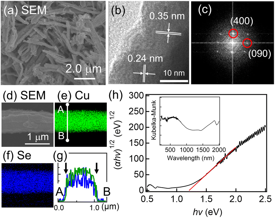 | ||
| Fig. 1 Characterization of copper selenide NWs synthesized using UV light irradiation for 12 hours. (a) A SEM image, (b) a HRTEM image, and (c) a FFT pattern. The arrows in (b) indicate lattice spacings of α-Cu2Se, corresponding to the α-Cu2Se (400) and (090) spots in (c). (d) SEM image and EDX mappings of (e) Cu and (f) Se. (g) Line profiles for a line segment A and B in (e). The green and blue profiles represent Cu and Se, respectively. (h) A plot of (αhν)1/2versus hν calculated from the DR UV-vis spectrum in the inset graph. | ||
Fig. 1d–f show the SEM-EDX mapping images. A bundle of multiple NWs was used for the EDX analysis to obtain a strong signal, as shown in Fig. 1d. From the mapping images, Cu and Se species were observed on NWs. To clarify the uniformity of constituent elements on NWs, line profiles in Fig. 1g were obtained for a line segment A and B in Fig. 1e and f. The intensity of Cu and Se species rose and dropped at the same position indicated by arrows. This indicates that Cu species were uniformly distributed along Se species on NWs.
The DR UV-vis-NIR spectrum of the α-Cu2Se NWs is shown in the inset of Fig. 1h, which indicates that the α-Cu2Se NWs exhibited optical absorption at a wavelength of <1000 nm. The optical absorption near the band edge follows the equation:42
| αhν = A(hν − Eg)n/2 | (2) |
Cu2+xSe NWs were also synthesized with various composition ratios. As shown in Fig. 2a, the composition ratio quantified by EDX (xq) exhibits a monotonically increasing trend in relation to x. This trend suggests the formation of Cu2+xSe NWs with various composition ratios. However, in the range of x > 0.0, the xq values were saturated and were consistently smaller than the corresponding x values. The missing Cu remained unreacted in solution, namely only Cu that can be soluble in Cu2Se reacted. Here, to investigate the presence and amounts of Cu vacancies in Cu2+xSe NWs, we obtained DR UV-vis-NIR spectra of these NWs. Fig. 2b shows the DR UV-vis-NIR spectra normalized by using the Kubelka–Munk values at around a 500 nm wavelength corresponding to band-edge or interband absorption.45 For x ≤ 0.0, additional broad peaks were observed at a longer wavelength than 800 nm, corresponding to intraband absorption.45 Intraband absorption is caused by electron excitation from a lower energy filled state to a higher energy empty state within the valence band, which is formed by the introduction of Cu vacancies.45 The intraband absorption peak (Cu vacancies) decreased on increasing x in Cu2+xSe NWs, as shown in Fig. 2b. Although there are small amounts of Cu vacancies for Cu2.00Se, the Cu vacancies almost disappeared for Cu2.10Se by adding a slight excess of Cu. The saturation of xq (Fig. 2a) was found to be due to the reduction of Cu vacancies brought about by the incorporation of excess Cu. The Cu vacancies affect the carrier concentrations (p) in Cu2+xSe NWs because Cu vacancies work as acceptors in Cu2Se. In fact, the p value of Cu1.95Se NWs (6.1 × 1021 cm−3) measured by Hall effect measurement was higher than that of Cu2.00Se NWs (1.8 × 1021 cm−3). This result also supports the decrease in the amounts of Cu vacancies in Cu2+xSe NWs on increasing x. From these results, Cu2+xSe NWs were precisely synthesized with various composition ratios by the photoreduction method.
 | ||
| Fig. 2 (a) The composition ratio quantified by EDX (xq) as a function of composition ratio (x). The dashed line in (a) indicates the theoretical one when xq is the same as x. (b) DR UV-vis-NIR spectra of Cu2+xSe NWs normalized by using the Kubelka–Munk values at around a 500 nm wavelength corresponding to band-edge or interband absorption. | ||
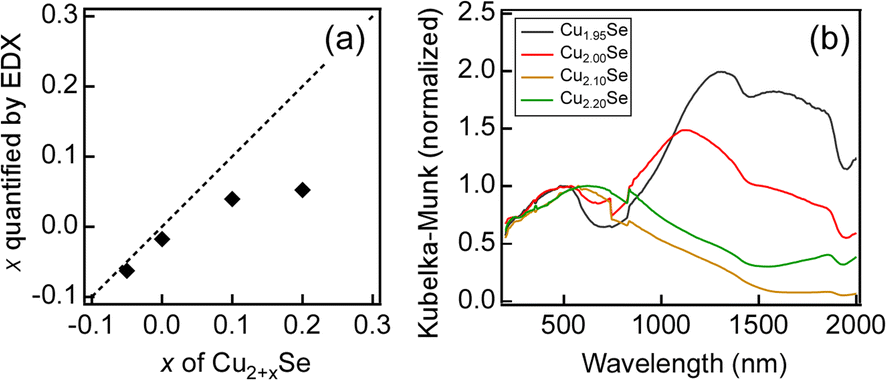
Fig. 3a–c show the composition ratio (x) dependencies of σ, S and S2σ of Cu2+xSe NWs measured at RT, respectively. σ and S of Cu2+xSe NWs monotonically decreased and increased as x increased, respectively. As a result, S2σ was maximized for Cu2.00Se NWs. The dependencies can be explained by the change in p in Cu2+xSe NWs. In general, there is a trade-off relationship between σ and S: σ increases and S decreases with the increase in p, and S2σ is maximized on optimizing p. In the case of Cu2+xSe NWs, S2σ was maximized by precisely synthesizing Cu2+xSe NWs with various composition ratios because p depends on the amounts of Cu vacancies. We abandoned the measurement of κ due to the subtle thickness and surface roughness of the Cu2+xSe NW films. However, κ of our Cu2+xSe NW films might be lower than that of Cu2Se bulks with uniform nanostructures because phonons with various mean free paths can be scattered at two types of interfaces: (1) polycrystalline interfaces and (2) NW/NW interfaces. The actual κ will be evaluated in future study.
 | ||
| Fig. 3 The composition ratio (x) dependencies of (a) σ, (b) S and (c) S2σ of Cu2+xSe NWs measured at RT. The dashed lines in a–c indicate eye-guides. (d) S2σ of Cu2.00Se NWs (solid symbol) as a function of the fabrication temperature. In (d), the data of polycrystalline films (open symbol)48–50 were plotted. | ||
Comparing the thermoelectric properties of Cu2+xSe NWs with those of previously reported bulk samples, S was comparable to that of the bulk samples while carrier mobility μ was lower than that of the bulk samples at the same carrier concentration22,46 (Fig. S3†). In general, the bulk samples synthesized at high temperature by the sintering or melting method exhibit higher carrier mobility due to low concentration of point defects and polycrystalline interfaces.47 In fact, bulk Cu2Se samples exhibit a high S2σ of ∼8 μW cm−1 K−2 at RT.22 To compare our Cu2+xSe NW samples synthesized at near RT with previously reported samples, we plotted S2σ data with thin films fabricated at relatively low temperature as a function of fabrication temperature as shown in Fig. 3d. Cu2+xSe NW samples exhibited comparable S2σ to that of the polycrystalline films fabricated at higher temperature.48–50 The achievement of the high S2σ despite low-temperature fabrication is attributed to the precise synthesis of Cu2+xSe NWs with various amounts of Cu vacancies. The S2σ values also followed the temperature trend of epitaxial films (Fig. S4†).51 Here, we suggest that the reason why Cu2+xSe NWs could be synthesized with various Cu vacancies is due to the precise reaction of Cu2+ and Se nanowires without additional Cu-related precipitates coming from the slow reaction of photoreduction. In the following section, we investigated the reaction process of Cu2.00Se NWs in detail by observing the reaction intermediates.
Reaction time dependences of 2θ-ω scans of XRD for Cu2.00Se NWs were observed as shown in Fig. S5.† To see the reaction time dependence simply, the enlarged graph of 20–35° was used for the analysis, as shown in Fig. 4a. The peaks indicated by star marks (★) for 12 h were found to be assigned to monoclinic α-Cu2Se. Since the observed pattern was entirely different from that for 0 h (as-prepared Se NWs) assigned to hexagonal Se, Se NWs completely reacted with Cu2+ ions for 12 h. No peaks originating from metallic Cu at 43.3°, Cu2O at 36.4° or CuO at 35.5° were observed (JCPDS file no. 5-0667 and 48–1548) (Fig. S5†). Looking at the XRD patterns for 0.5-6 h, various phases (hexagonal Se (●), hexagonal CuSe (▼), tetragonal Cu3Se2 (■), cubic β-Cu2Se (▲), and monoclinic α-Cu2Se (★)) were observed. From these XRD patters, typical peaks originating from CuSe + Se, Cu3Se2 + CuSe + β-Cu2Se, β-Cu2Se + Cu3Se2, α-Cu2Se, and α-Cu2Se were observed for 0.5, 2, 4, 6, and 12 h, respectively (Fig. 4b). Considering that the main peaks for 0.5, 2, 4, and 6 h were assigned to CuSe, Cu3Se2, β-Cu2Se, and α-Cu2Se, respectively, Se NWs were sequentially reacted with Cu2+ ions as follows:
| Se → CuSe → Cu3Se2 → β-Cu2Se → α-Cu2Se | (3) |
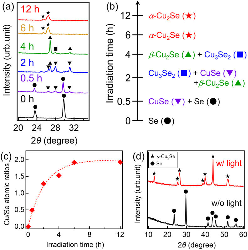 | ||
| Fig. 4 (a) 2θ-ω XRD scans for copper selenide NWs synthesized using UV light irradiation for 0–12 hours. (b) Crystal phases of copper selenide NWs as a function of light irradiation time. (c) Cu/Se atomic ratios obtained by quantitative EDX analysis as a function of light irradiation time. In (c), the dashed curve represents the fitted one to the experimental data with eqn (6). (d) 2θ-ω XRD scans for the samples with and without light irradiation for 12 hours. | ||
As these results show, α-Cu2Se NWs were formed through crystal structure changes by a sequential reaction as indicated by eqn (3). This sequential reaction of copper and selenium was also reported for the synthesis of copper selenides by the electrochemical method.52,53 It was found that similar reaction processes occurred for the synthesis of α-Cu2Se NWs through the photoreduction method. This result indicates that Cu2+ and Se NWs were precisely reacted without additional Cu-related precipitates, leading to the control of the amounts of Cu vacancies. Since the Cu2+xSe NWs used for the evaluations of thermoelectric properties and UV-vis-NIR were synthesized at 12 h, they were probably completely alloyed.
We also synthesized single phase β-Cu2Se or CuSe NWs with the Cu/Se atomic ratios of 1.8 or 1.0 by the photoreduction method, respectively. 2θ-ω XRD scans of these NWs are shown in Fig. S6.† The XRD peaks observed from NWs with a Cu/Se ratio of 1.8 and 1.0 were assigned to only cubic β-Cu2Se and hexagonal CuSe, respectively. This result indicates that targeted phases of copper selenide can be synthesized by adjusting Cu/Se ratios. We also found that S2σ of β-Cu2Se NWs and CuSe NWs was much lower than that of α-Cu2Se NWs (Fig. S7†). Namely, the control of the crystalline phase through the photoreduction method is one of the reasons why α-Cu2Se NWs exhibited a high S2σ in this study.
To elucidate the process of the reaction of Cu2+ ions and Se NWs, the reaction kinetics are discussed below. Cu/Se atomic ratios obtained by quantitative EDX analysis were plotted as a function of reaction time (Fig. 4c). The ratio was almost saturated to be ∼2 at 6 h. This result is consistent with XRD results, where single-phase α-Cu2Se was formed at 6 h. It is obvious that the Cu/Se data can be fitted using the following equation:
| Cu/Se = 2(1 − exp(−kt)) | (4) |
 | (5) |
 | (6) |
To investigate the effect of light irradiation, the same synthesis processes without light irradiation for 12 hours were also conducted. Fig. 4d shows 2θ-ω XRD scans for samples with and without light irradiation for 12 hours. In the sample without light irradiation, XRD patterns of only hexagonal Se were observed while those of other copper selenides such as monoclinic α-Cu2Se were not observed. Thus, Cu2+ ions and Se NWs could not be reacted without light irradiation. Therefore, these results support that photoreduction occurred with Cu+ ions adsorbed on Se NWs, as shown in Fig. 5a. Therefore, Cu2+ ions were sequentially reacted with Se NWs without deficiency. Namely, this photoreduction under the adsorbed conditions realized the control of Cu vacancies in Cu2+xSe NWs (Fig. 5a).
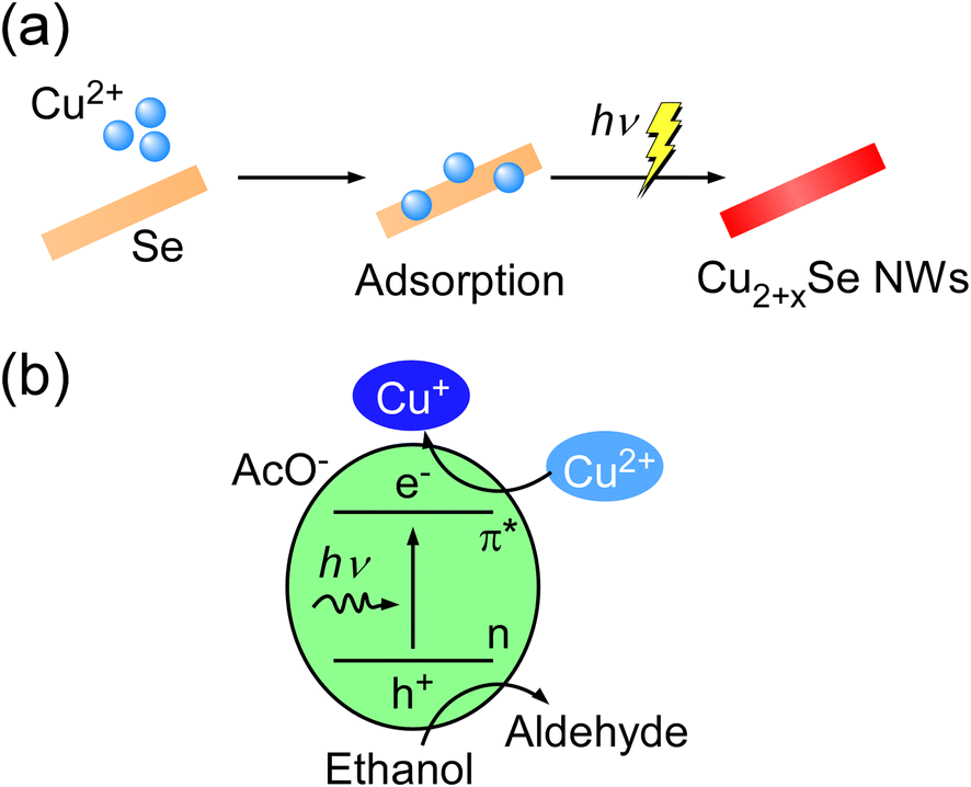 | ||
| Fig. 5 Schematic illustration of (a) the precise synthesis of Cu2+xSe NWs through photoreduction with Cu2+ ions adsorbed on Se NWs and (b) the photoreduction mechanism of Cu2+ ions. | ||
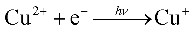
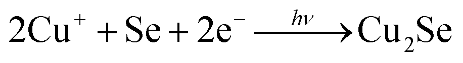
Finally, we show the mechanism of the photoreduction process. In our previous studies, Cu nanoparticles were synthesized by reducing copper ions through the photoreduction method.33 Therein, we consider that photoinduced electrons in acetic acid ions (AcO−) were transferred to copper ions according to the previous studies on the photoredox properties of copper(II)-carboxylate complexes.54–57 Given the consistent use of the same solvent (water and ethanol) and cuprous salt (copper acetate) in this study, the reduction of copper ions comes from the same mechanism observed in Cu nanoparticle formation, as illustrated in Fig. 5b. Notably, considering that the selenium valence in α-Cu2Se is −2,50,58 it is obvious that Se was also reduced by light irradiation.
Conclusions
We synthesized Cu2+xSe NWs with various amounts of Cu vacancies at RT by the photoreduction method and investigated their thermoelectric properties. Cu2+xSe NWs exhibited comparable S2σ to that of the polycrystalline films fabricated at higher temperature. The achievement of the high S2σ despite low-temperature fabrication is attributed to the precise synthesis of Cu2+xSe NWs with various amounts of Cu vacancies. From XRD analysis of the intermediate condition before complete reaction, it was found that Se NWs were consequently reacted with Cu2+ ions, accompanying changes in crystal structures, resulting in the formation of single-phase α-Cu2Se NWs. Furthermore, the discussion of reaction kinetics revealed that photoreduction occurred with Cu2+ ions adsorbed on Se NWs. Therefore, Cu2+ ions were sequentially reacted with Se NWs without deficiency. Namely, this photoreduction under the adsorbed conditions realized the control of Cu vacancies in Cu2+xSe NWs.Author contributions
S. S. conceptualization, methodology, formal analysis, funding acquisition, visualization, writing – original draft, writing – review & editing, T. M. data curation, investigation, K. M. data curation, investigation, Y. M. data curation, investigation, S. M. data curation, investigation, R. Y. data curation, T. S. data curation, A. A. data curation, H. U. writing – review & editing, and H. T. funding acquisition, supervision, writing – review & editing.Conflicts of interest
There are no conflicts to declare.Acknowledgements
This work was supported by Grant-in-Aid for Early-Career Scientists Grant Number 21K14479 and Grant-in-Aid for Scientific Research (C) Grant Number 19K05187 from JSPS KAKENHI, Japan. We are thankful for the assistance of Prof. K. Ohishi and Prof. H. Chang at Chuo University for cold pressing and XRD measurement, respectively.References
- W. Liu, X. Yan, G. Chen and Z. Ren, Recent Advances in Thermoelectric Nanocomposites, Nano Energy, 2012, 1, 42–56 CrossRef CAS.
- S. K. Bux, R. G. Blair, P. K. Gogna, H. Lee, G. Chen, M. S. Dresselhaus, R. B. Kaner and J. P. Fleurial, Nanostructured Bulk Silicon as an Effective Thermoelectric Material, Adv. Funct. Mater., 2009, 19, 2445–2452 CrossRef CAS.
- A. I. Hochbaum, R. Chen, R. D. Delgado, W. Liang, E. C. Garnett, M. Najarian, A. Majumdar and P. Yang, Enhanced Thermoelectric Performance of Rough Silicon Nanowires, Nature, 2008, 451, 163–167 CrossRef CAS PubMed.
- A. I. Boukai, Y. Bunimovich, J. T. Kheli, J. K. Yu, W. A. Goddard and J. R. Heath, Silicon Nanowires as Efficient Thermoelectric Materials, Nature, 2008, 451, 168–171 CrossRef CAS PubMed.
- G. Joshi, H. Lee, Y. Lan, X. Wang, G. Zhu, D. Wang, R. W. Gould, D. C. Cuff, M. Y. Tang, M. S. Dresselhaus, G. Chen and Z. Ren, Enhanced Thermoelectric Figure-of-Merit in Nanostructured p-type Silicon Germanium Bulk Alloys, Nano Lett., 2008, 8, 4670–4674 CrossRef CAS PubMed.
- X. W. Wang, H. Lee, Y. C. Lan, G. H. Zhu, G. Joshi, D. Z. Wang, J. Yang, A. J. Muto, M. Y. Tang, J. Klatsky, S. Song, M. S. Dresselhaus, G. Chen and Z. F. Ren, Enhanced Thermoelectric Figure of Merit in Nanostructured n-type Silicon Germanium Bulk Alloy, Appl. Phys. Lett., 2008, 93, 193121 CrossRef.
- K. Biswas, J. He, I. D. Blum, C. I. Wu, T. P. Hogan, D. N. Seidman, V. P. Dravid and M. G. Kanatzidis, High-performance Bulk Thermoelectrics with All-scale Hierarchical Architectures, Nature, 2012, 489, 414–418 CrossRef CAS PubMed.
- Y. Nakamura, M. Isogawa, T. Ueda, S. Yamasaka, H. Matsui, J. Kikkawa, S. Ikeuchi, T. Oyake, T. Hori, J. Shiomi and A. Sakai, Anomalous Reduction of Thermal Conductivity in Coherent Nanocrystal Architecture for Silicon Thermoelectric Material, Nano Energy, 2015, 12, 845–851 CrossRef CAS.
- Y. Nakamura, Nanostructure Design for Drastic Reduction of Thermal Conductivity While Preserving High Electrical Conductivity, Sci. Technol. Adv. Mater., 2018, 19, 31–43 CrossRef CAS PubMed.
- X. Zianni and D. Narducci, Synergy between Defects, Charge Neutrality and Energy Filtering in Hyper-doped Nanocrystalline Materials for High Thermoelectric Efficiency, Nanoscale, 2019, 11, 7667 RSC.
- K. Biswas, J. He, Q. Zhang, G. Wang, C. Uher, V. P. Dravid and M. G. Kanatzidis, Strained Endotaxial Nanostructures with High Thermoelectric Figure of Merit, Nat. Chem., 2011, 3, 160–166 CrossRef CAS PubMed.
- D. Souda, K. Shimizu, Y. Ohishi, H. Muta, T. Yagi and K. Kurosaki, High Thermoelectric Power Factor of Si–Mg2Si Nanocomposite Ribbons Synthesized by Melt Spinning, ACS Appl. Energy Mater., 2020, 3, 1962–1968 CrossRef CAS.
- M. Nomura, R. Anufriev, Z. Zhang, J. Maire, Y. Guo, R. Yanagisawa and S. Volz, Review of Thermal Transport in Phononic Crystals, Mater. Today Phys., 2022, 22, 100613 CrossRef CAS.
- S. Yamasaka, Y. Nakamura, T. Ueda, S. Takeuchi and A. Sakai, Phonon Transport Control by Nanoarchitecture Including Epitaxial Ge Nanodots for Si-based Thermoelectric Materials, Sci. Rep., 2015, 5, 14490 CrossRef CAS PubMed.
- R. Anufriev, A. Ramiere, J. Maire and M. Nomura, Heat Guiding and Focusing Using Ballistic Phonon Transport in Phononic Nanostructures, Nat. Commun., 2017, 8, 15505 CrossRef CAS PubMed.
- S. Sakane, T. Ishibe, K. Mizuta, M. Kashino, K. Watanabe, T. Fujita, Y. Kamakura, N. Mori and Y. Nakamura, Methodology of Thermoelectric Power Factor Enhancement by Nanoscale Thermal Management in Bulk SiGe Composites, ACS Appl. Energy Mater., 2020, 3, 1235–1241 CrossRef CAS.
- S. Sakane, T. Ishibe, K. Mizuta, T. Fujita, Y. Kiyofuji, J. Ohe, E. Kobayashi and Y. Nakamura, Anomalous Enhancement of Thermoelectric Power Factor by Thermal Management with Resonant Level Effect, J. Mater. Chem. A, 2021, 9, 4851–4857 RSC.
- D. Vashaee and A. Shakouri, Improved Thermoelectric Power Factor in Metal-Based Superlattices, Phys. Rev. Lett., 2004, 92, 106103 CrossRef PubMed.
- T. Ishibe, A. Tomeda, K. Watanabe, Y. Kamakura, N. Mori, N. Naruse, Y. Mera, Y. Yamashita and Y. Nakamura, Methodology of Thermoelectric Power Factor Enhancement by Controlling Nanowire Interface, ACS Appl. Mater. Interfaces, 2018, 10, 37709–37716 CrossRef CAS PubMed.
- S. Sakane, T. Ishibe, T. Taniguchi, N. Naruse, Y. Mera, T. Fujita, M. M. Alam, K. Sawano, N. Mori and Y. Nakamura, Thermoelectric Power Factor Enhancement Based on Carrier Transport Physics in Ultimately Phonon-Controlled Si Nanostructures, Mater. Today Energy, 2019, 13, 56–63 CrossRef.
- S. Sakane, T. Ishibe, Y. Yukawa and Y. Nakamura, Thermoelectric Properties of B-doped Nanostructured Bulk Diamond with Lowered Thermal Conductivity, Diam. Relat. Mater., 2023, 140, 110410 CrossRef CAS.
- J. Y. Tak, W. H. Nam, C. Lee, S. Kim, Y. S. Lim, K. Ko, S. Lee, W. S. Seo, H. K. Cho, J. H. Shim and C. H. Park, Ultralow Lattice Thermal Conductivity and Significantly Enhanced Near-Room-Temperature Thermoelectric Figure of Merit in α-Cu2Se through Suppressed Cu Vacancy Formation by Overstoichiometric Cu Addition, Chem. Mater., 2018, 30, 3276–3284 CrossRef CAS.
- S. D. Kang, S. A. Danilkin, U. Aydemir, M. Avdeev, A. Studer and G. J. Snyder, Apparent Critical Phenomena in the Superionic Phase Transition of Cu2-xSe, New J. Phys., 2016, 18, 013024 CrossRef.
- W. D. Liu, L. Yang, Z. G. Chen and J. Zou, Promising and Eco-Friendly Cu2X-Based Thermoelectric Materials: Progress and Applications, Adv. Mater., 2020, 32, 1905703 CrossRef CAS PubMed.
- Z. Zhang, K. Zhao, T. R. Wei, P. Qiu, L. Chen and X. Shi, Cu2Se-Based Liquid-like Thermoelectric Materials: Looking Back and Stepping Forward, Energy Environ. Sci., 2020, 13, 3307–3329 RSC.
- Y. Qin, L. Yang, J. Wei, S. Yang, M. Zhang, X. Wang and F. Yang, Doping Effect on Cu2Se Thermoelectric Performance: A Review, Materials, 2020, 13, 5704 CrossRef CAS PubMed.
- S. M. K. N. Islam, M. B. Cortie and X. Wang, Grape Juice: an Effective Liquid Additive for Significant Enhancement of Thermoelectric Performance of Cu2Se, J. Mater. Chem. A, 2020, 8, 16913 RSC.
- N. Chen, M. R. Scimeca, S. J. Paul, S. B. Hafiz, Z. Yang, X. Liu, F. Yang, D. K. Ko and A. Sahu, High-performance Thermoelectric Silver Selenide Thin Films Cation Exchanged From a Copper Selenide Template, Nanoscale Adv., 2020, 2, 368 RSC.
- L. Yang, Z. G. Chen, G. Han, M. Hong, Y. Zou and J. Zou, High-Performance Thermoelectric Cu2Se Nanoplates Through Nanostructure Engineering, Nano Energy, 2015, 16, 367–374 CrossRef CAS.
- H. Liu, X. Shi, F. Xu, L. Zhang, W. Zhang, L. Chen, Q. Li, C. Uher, T. Day and G. J. Snyder, Copper Ion Liquid-Like Thermoelectrics, Nat. Mater., 2012, 11, 422–425 CrossRef CAS PubMed.
- B. Yu, W. Liu, S. Chen, H. Wang, H. Wang, G. Chen and Z. Ren, Thermoelectric Properties of Copper Selenide with Ordered Selenium Layer and Disordered Copper Layer, Nano Energy, 2012, 1, 472–478 CrossRef CAS.
- S. Deka, A. Genovese, Y. Zhang, K. Miszta, G. Bertoni, R. Krahne, C. Giannini and L. Manna, Phosphine-Free Synthesis of p-Type Copper(I) Selenide Nanocrystals in Hot Coordinating Solvents, J. Am. Chem. Soc., 2010, 132, 8913 CrossRef PubMed.
- M. Miyagawa, T. Maeda, R. Tokuda, A. Shibusawa, T. Aoki, K. Okumura and H. Tanaka, Precious Metal-like Oxide-Free Copper Nanoparticles: High Oxidation Resistance and Geometric Structure, RSC Adv., 2016, 6, 104560–104565 RSC.
- M. Miyagawa, A. Shibusawa, K. Maeda, A. Tashiro, T. Sugai and H. Tanaka, Diameter-Controlled Cu Nanoparticles on Saponite and Preparation of Film by Using Spontaneous Phase Separation, RSC Adv., 2017, 7, 41896 RSC.
- M. Miyagawa, M. Usui, Y. Imura, S. Kuwahara, T. Sugai and H. Tanaka, Aqueous Synthesis of Protectant-Free Copper Nanocubes by a Disproportionation Reaction of Cu2O on Synthetic Saponite, Chem. Commun., 2018, 54, 8454 RSC.
- M. Miyagawa, Y. Ikeyama, H. Kotake, T. Maeda and H. Tanaka, Environmental-Friendly Degradation of Clay-Hybridized Cu Nanoparticles by Carboxylic Acids, Chem. Phys. Lett., 2020, 753, 137615 CrossRef CAS.
- M. Miyagawa, K. Nishino, A. Shibusawa, H. Kotake and H. Tanaka, Plasmonic Photoluminescence of Cu Nanoparticle Realized by Molecular Optical Antenna Designed on Nanosheets, Chem. Lett., 2022, 51, 500–503 CrossRef CAS.
- S. Sakane, T. Anji, I. Yamagishi, I. Kohara and H. Tanaka, Plasmonic Heating of Copper Nanoparticles with Thermoresponsive Polymers, Chem. Lett., 2023, 52, 582–585 CrossRef CAS.
- S. Sakane, K. Akimoto, K. Konishi, K. Takaoka, H. Iwatsuki, M. Akutsu, T. Sugai and H. Tanaka, Catalytic Activity of Non-aggregating Cu Nanoparticles Supported in Pores of Zeolite for Aerobic Oxidation of Benzyl Alcohol, ACS Omega, 2024, 9, 970–976 CrossRef CAS PubMed.
- S. Sakane, S. Miwa, T. Miura, K. Munakata, T. Ishide, Y. Nakamura and H. Tanaka, Thermoelectric Properties of PEDOT:PSS Containing Connected Copper Selenide Nanowires Synthesized by the Photoreduction Method, ACS Omega, 2022, 7, 32101–32107 CrossRef CAS PubMed.
- Q. Li and V. W. W. Yam, High-yield Synthesis of Selenium Nanowires in Water at Room Temperature, Chem. Commun., 2006, 1006–1008 RSC.
- B. Liu, L. Ning, H. Zhao, C. Zhang, H. Yang and S. Liu, Visible-light Photocatalysis in Cu2Se Nanowires with Exposed {111} Facets and Charge Separation Between (111) and (
![[1 with combining overline]](https://www.rsc.org/images/entities/char_0031_0305.gif) ) Polar Surfaces, Phys. Chem. Chem. Phys., 2015, 17, 13280–13289 RSC.
) Polar Surfaces, Phys. Chem. Chem. Phys., 2015, 17, 13280–13289 RSC. - Y. You, H. Hu and J. H. Choi, Atomic Adsorption on Monolayer Cu2Se: A First-Principles Study, Phys. Chem. Chem. Phys., 2021, 23, 9814–9821 RSC.
- A. P. Sudha, P. Prema, J. Henry, K. Mohanraj and G. Sivakumar, Influence of Trivalent (Bi, Sb) Metal Ions on the Photosensitivity of Doped Cu2Se Thin Films, J. Mater. Sci. Mater. Electron., 2017, 28, 6379–6387 CrossRef CAS.
- M. R. Scimeca, F. Yang, E. Zaia, N. Chen, P. Zhao, M. P. Gordon, J. D. Forster, Y. S. Liu, J. Guo, J. J. Urban and A. Sahu, Rapid Stoichiometry Control in Cu2Se Thin Films for Room-Temperature Power Factor Improvement, ACS Appl. Energy Mater., 2019, 2, 1517–1525 CrossRef CAS.
- J. Yu, K. Zhao, P. Qiu, X. Shi and L. Chen, Thermoelectric Properties of Copper-Deficient Cu2-xSe (0.05 ≤ x ≤ 0.25) Binary Compounds, Ceram. Int., 2017, 43, 11142–11148 CrossRef CAS.
- S. Sakane, T. Ishibe, T. Hinakawa, N. Naruse, Y. Mera, M. M. Alam, K. Sawano and Y. Nakamura, High Thermoelectric Performance in High Crystallinity Epitaxial Si Films Containing Silicide Nanodots with Low Thermal Conductivity, Appl. Phys. Lett., 2019, 115, 182104 CrossRef.
- Y. Li, Y. Zhong, D. Zhang, J. Niu, M. Nisar, M. Wei, G. Liang, P. Fan and Z. Zheng, Enhanced Thermoelectric Properties of Cu2Se Flexible Thin Films by Optimizing Growth Temperature and Elemental Composition, ACS Appl. Energy Mater., 2022, 5, 13964–13970 CrossRef CAS.
- P. Fan, X. Huang, T. Chen, F. Li, Y. Chen, B. Jabar, S. Chen, H. Ma, G. Liang, J. Luo, X. Zhang and Z. Zheng, α-Cu2Se Thermoelectric Thin Films Prepared by Copper Sputtering into Selenium Precursor Layers, Chem. Eng. J., 2021, 410, 128444 CrossRef CAS.
- L. Yang, J. Wei, Y. Qin, L. Wei, P. Song, M. Zhang, F. Yang and X. Wang, Thermoelectric Properties of Cu2Se Nano-Thin Film by Magnetron Sputtering, Materials, 2021, 14, 2075 CrossRef CAS PubMed.
- A. Wang, Y. Xue, J. Wang, X. Yang, J. Wang, Z. Li and S. Wang, High Thermoelectric Performance of Cu2Se-Based Thin Films with Adjustable Element Ratios by Pulsed Laser Deposition, Mater. Today Energy, 2022, 24, 100929 CrossRef CAS.
- C. Dai, L. Hu, H. Chen, X. Jin, Y. Han, Y. Wang, X. Li, X. Zhang, L. Song, M. Xu, H. Cheng, Y. Zhao, Z. Zhang, F. Liu and L. Qu, Enabling Fast-charging Selenium-based Aqueous Batteries via Conversion Reaction with Copper Ions, Nat. Commun., 2022, 13, 1863 CrossRef CAS PubMed.
- S. K. Sandstrom, H. Jiang, M. Lucero, Y. Xu, T. C. Gallagher, M. Cao, Z. Feng and X. Ji, Reversible Electrochemical Conversion from Selenium to Cuprous Selenide, Chem. Commun., 2021, 57, 10703–10706 RSC.
- J. Long, J. Dong, X. Wang, Z. Ding, Z. Zhang, L. Wu, Z. Li and X. Fu, Photochemical Synthesis of Submicron- and Nano-Scale Cu2O Particles, J. Colloid Interface Sci., 2009, 333, 791–799 CrossRef CAS PubMed.
- J. Y. Morimoto and B. A. Degraff, Photochemistry of the Copper(II)-Malonate System. A “Sensitized” Reaction, J. Phys. Chem., 1972, 76, 1387–1388 CrossRef CAS.
- J. Y. Morimoto and B. A. Degraff, Photochemistry of Copper Complexes. Copper(II) Malonate System, J. Phys. Chem., 1975, 79, 326–331 CrossRef CAS.
- P. Natarajan and G. Ferraudi, Photochemical Properties of Copper(II)-Amino Acid Complexes, Inorg. Chem., 1981, 20, 3708–3712 CrossRef CAS.
- S. Liu, Z. Zhang, J. Bao, Y. Lan, W. Tu, M. Han and Z. Dai, Controllable Synthesis of Tetragonal and Cubic Phase Cu2Se Nanowires Assembled by Small Nanocubes and Their Electrocatalytic Performance for Oxygen Reduction Reaction, J. Phys. Chem. C, 2013, 117, 15164–15173 CrossRef CAS.
Footnote |
| † Electronic supplementary information (ESI) available. See DOI: https://doi.org/10.1039/d4na00156g |
| This journal is © The Royal Society of Chemistry 2024 |