
 Open Access Article
 This Open Access Article is licensed under a Creative Commons Attribution-Non Commercial 3.0 Unported Licence
Sub-50 nm patterning of alloy thin films via nanophase separation for hydrogen gas sensing †
Sherjeel Mahmood
Baig
ab,
Satoshi
Ishii
 a and
Hideki
Abe
*ab
a and
Hideki
Abe
*ab
aNational Institute for Materials Science, 1-1 Namiki, 305-0044, Tsukuba, Ibaraki, Japan. E-mail: ABE.Hideki@nims.go.jp
bGraduate School of Science and Technology, Saitama University, 255 Shimookubo, Saitama 338-8570, Japan
First published on 17th April 2024
Abstract
A novel patterning method achieves two-dimensional nano-patterning of metal nanofibers by depositing a platinum–cerium alloy film on a silicon wafer and inducing phase separation in an oxygen–carbon monoxide atmosphere. The resulting nano-patterned thin film, Pt#CeO2/Si, consists of platinum and cerium oxide with an average pattern width of 50 nm and exhibits potential as a hydrogen sensor with sensitive electrical responses to hydrogen ad/desorption. The patterning method introduced herein addresses the challenge of wavelength limitations in traditional optical lithography, offering a scalable approach for sub-50 nm patterns, which are crucial for advanced sensor and electronic applications.
Introduction
Nano-patterned thin films play a pivotal role in optics, electronics, and sensing technologies. They are characterized by nanometre-wide metallic phases arranged in fibrous patterns on solid-state substrates such as silicon (Si) wafers.1 These films exhibit diverse patterns, including stripes, lattices, and networks.2 While several nanostructures have been implemented as a sensor head,3–8 nanonetwork-patterned thin films functioning as sensors for various chemical species capitalize on their high-density metal surfaces. Molecular ad/desorption on these surfaces can be detected in a highly sensitive manner as changes in electrical resistance within the nano-patterned network. This functionality positions network-patterned thin films as effective sensors with the potential to respond to various chemical stimuli across a range of applications.1,9Efforts to enhance the performance of patterned thin films are actively focused on reducing the patterning size. Lithography techniques, particularly those employing visible-light lasers, have been widely used to pattern metal thin films at the nanoscale, achieving patterns of around 100 nm.10 However, a challenge arises when attempting nano-patterning at sizes smaller than 50 nm, referred to as sub-50 nm patterning, as limitations imposed by the wavelength of light are encountered.11,12 Although techniques such as electron beam lithography (EBL) and focused ion beam lithography (FIB) can achieve sub-50 nm patterning, their adoption is limited by their low throughput due to intricate processes required and their use of ultra-fine manufacturing equipment.13 Block copolymer (BCP) lithography is a template-free patterning technique that represents a promising approach for nanolithography; nevertheless, its drawbacks such as material limitation, direct assembly and pattern transferring pose significant challenges for achieving sub-50 nm feature sizes with high fidelity and yield.14
Herein, we report that thin films can be patterned at the nanoscale by taking advantage of the spontaneous nanophase separation of alloys.15–17 Thin films of an alloy of platinum (Pt) and cerium (Ce), Pt–Ce, were deposited on Si substrates at a thickness of 50 nm using vacuum sputtering. Pt–Ce alloy thin films were then subjected to a stream of a gas mixture of carbon monoxide (CO) and oxygen (O2) at elevated temperatures to promote the selective oxidation of Ce (Fig. 1). As a result of the selective oxidation of the Pt–Ce film, a two-dimensional, fibrous nano-network of Pt and cerium dioxide, i.e., Pt#CeO2/Si, emerged, covering the Si surface (Fig. S1 and S2†). A set of gold-titanium (Au–Ti) terminals was finally deposited onto Pt#CeO2/Si, maintaining a gap of 25 μm. Pt#CeO2/Si exhibited a reversible change in two-terminal resistance when exposed to hydrogen (H2) and O2 atmospheres in sequence due to the adsorption of the various chemical species onto the Pt nano-network. The demonstrated chemo-electric function of Pt#CeO2/Si positions it as a potential alternative to traditional palladium (Pd)-based H2 sensors18,19 with the added advantage of reduced material costs (Pt cost: $28 per g compared to Pd cost: $40 per g).
 | ||
| Fig. 1 Schematic diagram illustrating the proposed nanopatterning method. A thin film of Pt–Ce alloy is deposited onto a Si substrate through vacuum sputtering (left). Ce and Pt atoms in the Pt–Ce film are represented by red and green circles, respectively (middle). The Pt–Ce film undergoes treatment in an O2-containing atmosphere, resulting in the formation of a nanonetwork composed of Pt and CeO2, with an average width of 50 nm (right); the maze-like red and green phases correspond to Pt and CeO2, respectively. | ||
Experimental
A sputtering target of Pt2Ce alloy was prepared by melting Pt and Ce metal ingots in an atomic ratio of Pt![[thin space (1/6-em)]](https://www.rsc.org/images/entities/char_2009.gif) :Ce = 2:1 using an arc torch in a pure Ar atmosphere (see powder X-ray diffractometry (pXRD) data in Fig. S3†). Thin films of the Pt–Ce alloy with an approximate thickness of 50 ± 1 nm were deposited onto a Si substrate (Si wafer: 380 μm thick) at room temperature through sputtering of the Pt2Ce target with an (MB-501010) electron-beam evaporator (Fig. S4 and S5†). The as-deposited Pt–Ce film exhibited chemical stability in air at room temperature and/or in a pure argon (Ar) atmosphere up to 600 °C (Fig. S6†). Subsequently, the Pt–Ce film underwent an atmosphere treatment in a stream of a gas mixture of CO, O2, and Ar in a specific volumetric ratio of 2 ml min−1, 1 ml min−1, and 47 ml min−1, respectively, at 600 °C for 1 hour.
:Ce = 2:1 using an arc torch in a pure Ar atmosphere (see powder X-ray diffractometry (pXRD) data in Fig. S3†). Thin films of the Pt–Ce alloy with an approximate thickness of 50 ± 1 nm were deposited onto a Si substrate (Si wafer: 380 μm thick) at room temperature through sputtering of the Pt2Ce target with an (MB-501010) electron-beam evaporator (Fig. S4 and S5†). The as-deposited Pt–Ce film exhibited chemical stability in air at room temperature and/or in a pure argon (Ar) atmosphere up to 600 °C (Fig. S6†). Subsequently, the Pt–Ce film underwent an atmosphere treatment in a stream of a gas mixture of CO, O2, and Ar in a specific volumetric ratio of 2 ml min−1, 1 ml min−1, and 47 ml min−1, respectively, at 600 °C for 1 hour.
Results and discussion
X-ray photoemission spectroscopy (XPS) was conducted to examine the chemical nature of as-deposited and atmosphere-treated Pt–Ce films (Fig. 2). In (a), the black curve represents pure Pt, and the red curve represents the film after atmospheric treatment; in (b), the black, red, and blue curves represent CeO2, the Pt–Ce film after atmospheric treatment, and the Pt–Ce film before treatment, respectively. Peak positions for 4f7/2- and 4f5/2 emissions from the atmosphere-treated Pt–Ce film exhibited a 0.20 eV shift towards deeper binding energies with respect to corresponding peaks from pure Pt (Fig. 2a).20,21 This shift in the Pt 4f emission peaks suggests that Pt atoms are partially deprived of valence electrons by adjacent oxygen (O) atoms, which are more electrophilic than Pt. The XPS spectrum of the atmosphere-treated Pt–Ce film closely resembles that of the control material, CeO2, in terms of the peak positions and intensities (Fig. 2b). Based on the XPS analyses in Pt- and Ce core regions, we conclude that the atmosphere-treated Pt–Ce film is a composite of Pt and CeO2 phases, where the Pt phase maintains atomistic contact with the CeO2 phase through Pt–O bonds.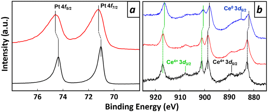 | ||
| Fig. 2 XPS spectra in the Pt 4f region (a) and Ce 3d region (b) for deposited films and the control. In (a), black and red curves represent pure Pt and the atmosphere-treated film, respectively. In (b), black, red, and blue curves correspond to CeO2, the atmosphere-treated Pt–Ce film, and the as-deposited Pt–Ce film, respectively. | ||
In the Ce 3d spectrum of the as-deposited Pt–Ce film, there is a recognizable finite shift in the peak positions towards binding energies 0.61 eV shallower than those for CeO2 or the atmosphere-treated Pt–Ce film (Fig. 2b).22 This shift indicates that Ce atoms in the as-deposited Pt–Ce film exist in a low valence state, as in metals. Note that a peak appears in the Ce 3d spectrum of the as-deposited film, which is attributed to Ce0 atoms in alloys such as CePd3.23 The low-valence Ce atoms in the as-deposited film undergo selective oxidation to CeO2 through the atmosphere treatment. This results in a phase separation to form a composite of the Pt and CeO2 phases. This transformation is accompanied by the formation of the Pt–O bonds, solidifying the interconnected structure of the Pt and CeO2 phases in the film.
Scanning electron microscopy (SEM) showed the uniformity of the as-deposited Pt–Ce film (Fig. 3a). Energy-dispersive X-ray spectroscopy (EDX) mapping confirmed a uniform distribution of Pt and Ce throughout the as-deposited film. The atomic ratio of Pt and Ce was determined to be Pt/Ce = 1.95 ± 0.05, with no traces of other elements present (Fig. S7, S8, and Table S9†). In contrast, nanophase separation became evident in the atmosphere-treated Pt–Ce film (Fig. 3b and c, see also Fig. S10 and S11† for more details on the nanophase separation). Fibrous Pt phases formed an interconnected network with a width of less than 40 nm, developing a two-dimensional nano-network of Pt metal. This metal nano-network allowed the Si substrate to be visible between adjacent Pt phases, resulting in a negative image of Pt distribution (Fig. 3c). Ce and O were mainly concentrated over the Pt phase. The average atomic ratio of Pt and Ce as quantified using EDX was Pt/Ce = 1.86 ± 0.05 (Fig. S12, and Table S13†). Hereafter, the nano-pattern of Pt and CeO2 that is spontaneously formed over the Si surface is denoted as Pt#CeO2/Si.
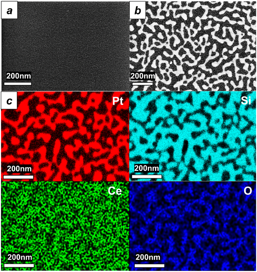 | ||
| Fig. 3 SEM images of the as-deposited Pt–Ce film (a) and atmosphere-treated Pt–Ce film (b). EDX mapping images of the atmosphere-treated Pt–Ce film (c), in which red, cyan, green, and blue images represent the elemental mapping of Pt, Si, Ce, and O, respectively. | ||
Kelvin-force probe microscopy (KFPM)24,25 was employed to investigate the surface potential distribution of Pt#CeO2/Si. A finely pointed platinum needle served as the KFPM probe. In Fig. 4, warm-colored areas indicate low surface potential, while cold-colored areas signify high surface potential. The warm-colored areas were assigned to the surfaces of the Si substrate, while the cold-colored areas correspond to the Pt phase. The Pt nano-network of Pt#CeO2/Si with low surface potential can act as an effective adsorption site for various molecules due to strong molecular dipole-surface dipole interactions. The Pt nano-network develops an interconnected electrical network throughout Pt#CeO2/Si, adding functionality as a sensitive electric probe for different gas species.
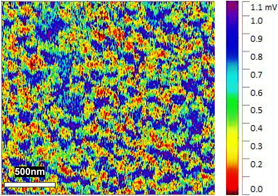 | ||
| Fig. 4 KPFM image of Pt#CeO2/Si, where the contrast from cold to warm colors visualizes the surface potential of the sample relative to the Pt probe surface. | ||
Finally, the Pt#CeO2 film was utilized as a gas-sensing probe. Using an electron-beam evaporator (UEP-3000BS), a pair of gold-titanium (Au–Ti) terminals was deposited onto the film surface, maintaining a terminal gap of 25 μm (Fig. S14†). The electrical resistance between these electrodes on Pt#CeO2/Si was measured through the two-terminal method (Fig. S15†). The resistivity of Pt#CeO2/Si increased as the temperature decreased (Fig. 5a). The trend in the temperature-dependence of the electrical resistance shows that the Pt metal nano-network in Pt#CeO2/Si was not entirely connected across the terminal gap, leading to semiconducting conduction rather than metallic conduction.
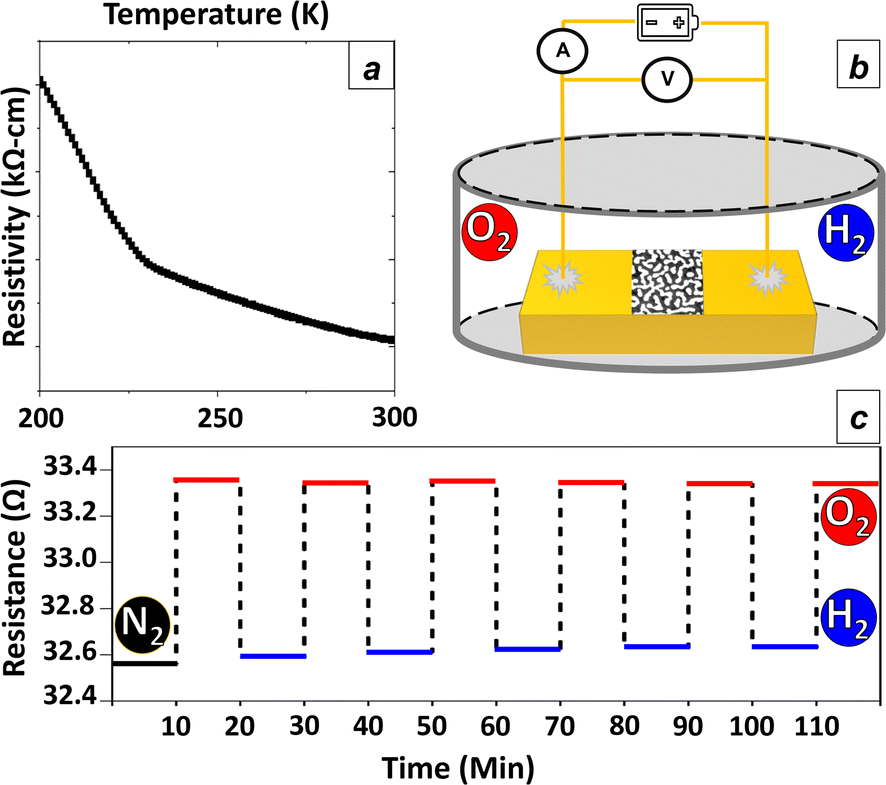 | ||
| Fig. 5 (a) Resistivity of Pt#CeO2/Si at different temperatures. (b) Schematic diagram of the hydrogen sensor setup featuring Pt#CeO2/Si. Pt#CeO2/Si with Au–Ti terminals was placed in a glass chamber with gas ports. Gold wires led electric terminals to an external current source, allowing monitoring of the inter-terminal voltage. (c) Electrical resistance of Pt#CeO2/Si at room temperature in various gas atmospheres, with figure annotations indicating the correspondence between gas type and resistance. | ||
Pt#CeO2/Si was then introduced into a glass chamber equipped with gas ports for inlet and outlet gases, as illustrated in the experimental setup scheme (Fig. 5b). Nitrogen (N2) gas was initially purged into the chamber to clean the surface of Pt#CeO2/Si before gas sensing tests. The electrical resistance of Pt#CeO2/Si was continuously monitored while hydrogen (H2) and oxygen (O2) were alternately injected into the sensing chamber for 5 minutes each (Table S16†). During exposure to the H2 gas atmosphere, the Pt surface of the Pt#CeO2 film adsorbed molecular H2, resulting in reduced electric resistance of the Pt nano-network due to the inhibited electron scattering as shown in Fig. 5c.26
When the hydrogen (H2) atmosphere was replaced by an O2 atmosphere, O2 molecule occupied the Pt surface, displacing physisorbed H2 molecules. The resistance of Pt#CeO2/Si was restored to its initial value during the first O2 purge (Fig. S17†). This cyclic change in electrical resistance was consistently observed each time the H2 and O2 atmospheres were alternated.27,28 Importantly, the switching of the atmospheres induced no irreversible change in resistance, underscoring the reversible nature of terminalized Pt#CeO2/Si as a reliable probe for H2 sensing.
Conclusion
In summary, our work leveraged the nanophase separation phenomenon in alloys to successfully fabricate thin metallic films with a network structure, achieving dimensions below 50 nm, which is challenging using traditional optical lithography methods. By depositing a Pt and Ce alloy thin film onto a Si substrate and subjecting it to an atmosphere containing O2 and CO at elevated temperatures, selective oxidation of Ce to CeO2 occurred, resulting in the emergence of a network-like Pt nano-pattern over the Si surface, denoted as Pt#CeO2/Si. The most appropriate temperature and time required for the formation of the most suitable nano-networks in terms of connectivity and reasonable separation were selected (Fig. S18†). Those Pt nano-patterns were uniformly spaced approximately 50 nm apart. Pt#CeO2/Si exhibited sensitive and repeatable responses in electrical resistance to the alternating cycles of O2 and H2 atmospheres, showcasing its potential as a probe in H2 gas sensors with robust detection at different concentrations of H2 (Table S19† and Fig. S20†) and high selectivity (Table S21† and Fig. S22†). The innovative nano-patterning method reported in this work holds promise as a breakthrough for diverse applications, including catalysts, sensors, optical collectors, and integrated circuits. Its simplicity, avoiding the need for complex and expensive lithography equipment, enables the construction of uniform nanostructures over large areas.Author contributions
S. M. Baig synthesized, characterized, and developed the chemo-electric functionality of the materials. S. Ishii conducted microscopic characterizations with S. M. Baig. H. Abe designed and conducted the research and edited the manuscript.Conflicts of interest
There are no conflicts to declare.Acknowledgements
This work was supported by “Advanced Research Infrastructure for Materials and Nanotechnology in Japan (ARIM)” of the Ministry of Education, Culture, Sports, Science and Technology (MEXT)—proposal number JPMXP1223NM5363.References
- H. Yin, K. Xing, Y. Zhang, D. M. A. S. Dissanayake, Z. Lu, H. Zhao, Z. Zeng, J.-H. Yun, D.-C. Qi and Z. Yin, Chem. Soc. Rev., 2021, 50, 6423–6482 RSC.
- H.-N. Barad, H. Kwon, M. Alarcón-Correa and P. Fischer, ACS Nano, 2021, 15, 5861–5875 CrossRef CAS PubMed.
- C. Hou, G. Tai, Y. Liu and X. Liu, Nano Res., 2022, 15, 2537–2544 CrossRef CAS.
- C. Hou, G. Tai, Y. Liu, R. Liu, X. Liang, Z. Wu and Z. Wu, Nano Energy, 2022, 97, 107189 CrossRef CAS.
- C. Hou, G. Tai, Y. Liu, Z. Wu, X. Liang and X. Liu, Nano Res. Energy, 2023, 2, e9120051 CrossRef.
- C. Hou, G. Tai, B. Liu, Z. Wu and Y. Yin, Nano Res., 2021, 14, 2337–2344 CrossRef CAS.
- C. Hou, G. Tai, Y. Liu, Z. Wu, Z. Wu and X. Liang, J. Mater. Chem. A, 2021, 9, 13100–13108 RSC.
- Z. Wu, G. Tai, R. Liu, W. Shao, C. Hou and X. Liang, J. Mater. Chem. A, 2022, 10, 8218–8226 RSC.
- T. Zhou and T. Zhang, Small Methods, 2021, 5, e2100515 CrossRef PubMed.
- M. Guo, Z. Qu, F. Min, Z. Li, Y. Qiao and Y. Song, InfoMat, 2022, 4, e12323 CrossRef CAS.
- Y. Wu and Z. Xiao, The Recent Progress of Lithography Machine and the State-of-art Facilities, Highlights in Science, Engineering and Technology, 2022 Search PubMed.
- T. Ito and S. Okazaki, Nature, 2000, 406, 1027–1031 CrossRef CAS PubMed.
- I. Kostic, K. Vutova, A. Bencurova, A. Ritomsky and R. Andok, in 2017 40th International Spring Seminar on Electronics Technology (ISSE), IEEE, 2017, pp. 1–6 Search PubMed.
- M. Guo, Z. Qu, F. Min, Z. Li, Y. Qiao and Y. Song, InfoMat, 2022, 4, e12323 CrossRef CAS.
- A. S. B. M. Najib, X. Peng, A. Hashimoto, S. Shoji, T. Iida, Y. Bai and H. Abe, Chem.–Asian J., 2019, 14, 2802–2805 CrossRef CAS PubMed.
- S. Shoji, X. Peng, T. Imai, P. S. Murphin Kumar, K. Higuchi, Y. Yamamoto, T. Tokunaga, S. Arai, S. Ueda, A. Hashimoto, N. Tsubaki, M. Miyauchi, T. Fujita and H. Abe, Chem. Sci., 2019, 10, 3701–3705 RSC.
- Y. Wen, H. Abe, K. Mitsuishi and A. Hashimoto, Nanoscale, 2021, 13, 18987–18995 RSC.
- I. Darmadi, F. A. A. Nugroho and C. Langhammer, ACS Sens., 2020, 5, 3306–3327 CrossRef CAS PubMed.
- K. Arora and N. K. Puri, Mater. Chem. Phys., 2020, 247, 122850 CrossRef CAS.
- C. J. Powell, J. Electron Spectrosc. Relat. Phenom., 2012, 185, 1–3 CrossRef CAS.
- P. Légaré, G. Lindauer, L. Hilaire, G. Maire, J.-J. Ehrhardt, J. Jupille, A. Cassuto, C. Guillot and J. Lecante, Surf. Sci., 1988, 198, 69–78 CrossRef.
- E. Paparazzo, G. M. Ingo and N. Zacchetti, J. Vac. Sci. Technol., A, 1991, 9, 1416–1420 CrossRef CAS.
- J. C. Fuggle, M. Beyss, M. Campagna, F. Steglich and F. Hulliger, X-Ray Photoemission From Ce Core Levels Of Cepd3, Cese, Ceal2 And Cecu2si2, Physica B+C, 1980, 102, 360–366 CrossRef.
- W. Melitz, J. Shen, A. C. Kummel and S. Lee, Surf. Sci. Rep., 2011, 66, 1–27 CrossRef CAS.
- G. Cohen, E. Halpern, S. U. Nanayakkara, J. M. Luther, C. Held, R. Bennewitz, A. Boag and Y. Rosenwaks, Nanotechnology, 2013, 24, 295702 CrossRef CAS PubMed.
- E. H. Sondheimer, Adv. Phys., 1952, 1, 1–42 CrossRef.
- H. W. Yoo, S. Y. Cho, H. J. Jeon and H. T. Jung, Anal. Chem., 2015, 87, 1480–1484 CrossRef CAS PubMed.
- N. Kilinc, J. Mater. Sci.: Mater. Electron., 2021, 32, 5567–5578 CrossRef CAS.
Footnote |
| † Electronic supplementary information (ESI) available. See DOI: https://doi.org/10.1039/d4na00071d |
| This journal is © The Royal Society of Chemistry 2024 |