
 Open Access Article
 This Open Access Article is licensed under a Creative Commons Attribution-Non Commercial 3.0 Unported Licence
Visible–ultraviolet dual-band photodetectors based on an all-inorganic CsPbCl3/p-GaN heterostructure†
Bingjie
Ye
a,
Boxiang
Wang
a,
Yan
Gu
a,
Jiarui
Guo
a,
Xiumei
Zhang
a,
Weiying
Qian
a,
Xiangyang
Zhang
a,
Guofeng
Yang
 *a,
Zhixing
Gan
*b and
Yushen
Liu
*c
*a,
Zhixing
Gan
*b and
Yushen
Liu
*c
aSchool of Internet of Things Engineering, Jiangnan University, Wuxi 214122, China. E-mail: gfyang@jiangnan.edu.cn
bCenter for Future Optoelectronic Functional Materials, School of Computer and Electronic Information/School of Artificial Intelligence, Nanjing Normal University, Nanjing 210023, China. E-mail: zxgan@njnu.edu.cn
cYancheng Polytechnic College, Yancheng 224005, China. E-mail: ysliu@yctei.edu.cn
First published on 22nd April 2024
Abstract
All-inorganic metal halide perovskites (MHPs) have attracted increasing attention because of their high thermal stability and band gap tunability. Among them, CsPbCl3 is considered a promising semiconductor material for visible–ultraviolet dual-band photodetectors because of its excellent photoelectric properties and suitable band gap value. In this work, we fabricated a visible–ultraviolet dual-band photodetector based on a CsPbCl3/p-GaN heterojunction using the spin coating method. The formation of the heterojunction enables the device to exhibit obvious dual-band response behavior at positive and negative bias voltages. At the same time, the dark current of the device can be as low as 2.42 × 10⁻⁹ A, and the corresponding detection rate can reach 5.82 × 10¹⁰ Jones. In addition, through simulation calculations, it was found that the heterojunction has a type II energy band arrangement, and the heterojunction response band light absorption is significantly enhanced. The type II energy band arrangement will separate electron–hole pairs more effectively, which will help improve device performance. The successful implementation of visible–ultraviolet dual-band photodetectors based on a CsPbCl3/p-GaN heterojunction provides guidance for the application of all-inorganic MHPs in the field of multi-band photodetectors.
Introduction
Organic–inorganic hybrid perovskites have been used in optoelectronic devices such as solar cells,1–3 light-emitting diodes,4–6 and photodetectors7–9 because of their large absorption coefficient, long photogenerated carrier lifetime, and high carrier mobility. However, the thermal instability of their organic components hinders their practical application.10 The emergence of all-inorganic metal halide perovskites (MHPs) well compensates for this defect. By substituting inorganic atoms for organic components in hybrid perovskites, all-inorganic MHPs not only have high thermal stability,11–13 but also have certain bandgap tunability.14–16Multi-band photodetectors, which can distinguish the intended target in the clutter and enhance the target signal, have attracted extensive attention. In a complex environment, the detection system uses a single distinguishable spectral response to collect different information in multiple targets for analysis through the multi-band photodetection capability of a single device.17–19 In this case, a monolithic device with excellent multi-wavelength photodetection capability is particularly important for the whole system. The emerging all-inorganic perovskite CsPbCl3 has excellent optoelectronic properties and a suitable bandgap value, and is considered to be a promising semiconductor material for high-performance visible-blind ultraviolet dual-band photodetection.20 As the application fields of multi-band photodetectors continue to expand, including in environmental sensors, optical communications,21,22etc., the performance requirements of photodetectors are also constantly increasing.
Combination with other semiconductor materials to construct heterojunctions is considered to be an effective way to adjust optoelectronic performance and improve light utilization efficiency through energy band engineering.23–25 So far, many all-inorganic MHPs have formed heterojunctions with other materials and significantly improved their photodetection capabilities. Algadi et al.26 significantly improved charge extraction at the heterojunction interface by combining CsPbBr3 with carbon nanodots to form high-band alignment between them. In addition, the carbon nanodots accelerated the extraction of electrons and holes in the CsPbBr3 film, thereby shortening the response time of the photodetector. Lu et al.27 combined CsPbBr3 with In2S3 to form a type II energy band alignment, blocking interlayer carrier coupling and achieving spatial separation of photogenerated carriers through quantum tunneling. At the same time, the heterostructure makes the Pb–Br bond not easy to break, which enhances the environmental stability of the device. Compared with other perovskite photodetectors, CsPbCl3 photodetectors were studied relatively late. In 2017, Liu et al.28 used CsPbCl3 nanocrystals as light absorbers to propose a photoconductive CsPbCl3 photodetector for the first time. Limited by the grain boundaries and recombination loss in the layer, the device did not show excellent performance. A novel sequential evaporation deposition strategy was developed by Zhan et al.29 to introduce a PbS buffer layer. In this process, a PbCl2 precursor layer was first evaporated onto an indium tin oxide (ITO) substrate, and then a CsCl layer of a different thickness was evaporated onto the PbCl2 film, and the phase composition of the resulting CsPbCl3 film was adjusted by adjusting the thickness of CsCl. The PbS buffer layer can not only passivate the surface defects of the CsPbCl3 layer, but also form a type II heterojunction with CsPbCl3 to lower the interfacial energy barrier, thus contributing to a faster hole extraction rate and suppressed dark current level. However, the requirements for evaporative deposition on the environment and equipment, as well as the control of the thickness of the precursor and CsCl during the deposition process are not simple. Therefore, finding suitable semiconductor materials for easy and effective combination with CsPbCl3 and exploring its mechanism of action are very important for the application of CsPbCl3 in high-performance multi-band photodetectors.
GaN is considered to be the most promising candidate material for UV photodetectors because of its wide direct bandgap, high breakdown voltage, large absorption coefficient, and high carrier mobility.30 So far, a variety of materials have been combined with GaN to form heterojunctions and improve the performance of the detector's switching ratio and responsivity through direct evaporation deposition, mechanical exfoliation and other simple experimental methods.31–33 Notably, many of these devices achieved dual-wavelength responses in addition to outperforming single-material devices. Solanke et al.34 achieved a dual-wavelength response of 365 nm and 850 nm by exfoliating α-In2Se3 tape onto a GaN substrate. At a bias voltage of −3 V, the normalized responsivity values at 365 nm and 850 nm were both about 70 mA W−1, the photo-dark current ratio is about 665 and 75 in turn, and the estimated specific detectivity values are about 1011 Jones and 1010 Jones, respectively.
In this work, CsPbCl3 nanocrystals were spin-coated onto GaN substrates to form a CsPbCl3/p-GaN heterojunction for broadband photoresponse. The macroscopic orientation, optical properties and surface morphology of the material were characterized by XRD, PL, the absorption spectrum, SEM, TEM and EDS spectra. In addition, by making the heterojunction a photodetector, the measured dark current of the device is as low as 2.31 × 10⁻⁸ A at −2 V. The device is irradiated with 365 nm and 420 nm light, and the obvious optical gain current curve is obtained. When the voltage was fixed and the wavelength of the irradiated light was changed, an obvious dual-band photoresponse behavior was observed at 365 nm and 420 nm. At the same time, the QuantumATK simulation software was used to simulate the energy band diagram, energy band projection density of states and optical absorption coefficient of the heterojunction to explain the photoresponse behavior of the device at different bias voltages. The successful realization of the device's dual-band photoresponse plays an important guiding role in the exploration of all-inorganic MHPs in the field of dual-band photoresponse photodetectors.
Methods
The p-GaN substrate used in this experiment was epitaxially grown on a sapphire substrate through metal–organic chemical vapor deposition (MOCVD). Fig. 1(a) shows a schematic diagram of the structure of the p-GaN substrate, which consists of a sapphire substrate, a 50 nm-thick AlN buffer layer, a 2.5 μm-thick undoped GaN epitaxial layer and 300 nm-thick p-type GaN formed by Mg doping, in which the Mg doping concentration is 1 × 1019 cm−3. In recent years, the spin coating method has been widely used in the preparation of nanomaterials because of its low cost, easy operation, and excellent uniformity and compactness of nanomaterials.35,36 The experiment in this work applies the spin-coating method for the preparation of a CsPbCl3/p-GaN heterojunction, as shown in Fig. 1(b).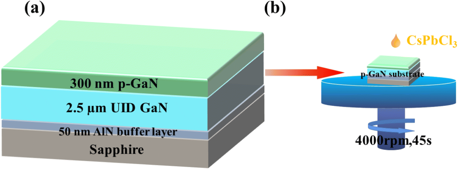 | ||
| Fig. 1 (a) Epitaxial diagram of the p-GaN substrate; (b) spin coating process of CsPbCl3 nanocrystals. | ||
The first step in the spin coating method is to prepare the precursor solution, and CsPbCl3 precursor solution was prepared according to previous reports.16 First, Cs2CO3 (0.814 g, 99.9%) was placed in a 100 mL three-necked flask together with octadecene (ODE) (30 mL, 90%) and oleic acid (OA) (2.5 mL, 90%), and the mixture was dried at 120 °C under N2 for 2 hours. Then the temperature of the solution was reduced to 100 °C. ODE (75 mL), oleylamine (OLA) (7.5 mL, 90%), dried OA (7.5 mL) and PbCl2 (0.675 g, 99.99%) were loaded into a 250 mL three-neck flask and dried under vacuum for 2 h at 120 °C. After the PbCl2 salt was completely dissolved, the temperature was increased to 170 °C, and the Cs-oleate solution prepared as described above was rapidly injected. After 10 seconds, the reaction mixture was cooled in an ice water bath. In this experiment, 1 mL of trioctylphosphine (TOP) (ninety-seven percent) was added to dissolve PbCl2 to synthesize CsPbCl3. Nanocrystals were precipitated from the solution by centrifugation at 7000 rpm for 5 minutes. After centrifugation, the supernatant was discarded, and the nanocrystals were redispersed in anhydrous hexane (99%), and further centrifuged at 3000 rpm for 1 minute to precipitate again to remove impurities. Subsequently, as shown in Fig. 1(a), CsPbCl3 nanocrystals were combined with the p-GaN substrate shown in Fig. 1(b) by using a simple spin-coating method at 4000 rpm for 45 seconds. Finally, the CsPbCl3/p-GaN heterojunction was obtained by thermal annealing. After material characterization, Ni/Au was deposited on CsPbCl3 and GaN by thermal evaporation to make device electrodes.
The optical properties of the materials are characterized by using absorption and photoluminescence (PL) spectra (Renishaw LabRAM Inviamicro-Raman system). In addition, SEM (FE-SEM: JEOL JSM-7000F), TEM (FEI Tecnai F20), XRD (PA Nalytical X'Pert Pro MRD) and EDS mapping were used to characterize the surface morphology, lattice type, crystal plane macro-orientation, element distribution and other material properties of the sample. Meanwhile, the I–V characteristics, photoresponse and transient photoresponse of the CsPbCl3/p-GaN heterojunction photodetector were all measured by using a probe station equipped with a semiconductor parameter analyzer (Keithley 4200-SCS).
In this experiment, the QuantumATK software package was used to construct and optimize the CsPbCl3/GaN heterojunction, followed by its performance simulation. A Pseudo Dojo pseudopotential37 optimization structure was adopted in the process of constructing materials and heterojunctions, and the cutoff energy was set to 95 Hartree. In the material optimization parameters, the maximum interatomic stress was set to 0.01 eV Å−1, and the maximum energy difference convergence limit was set to 10−5 eV. In order to better simulate the electrical and optical properties of layered CsPbCl3 and GaN heterojunctions, multilayer CsPbCl3 was constructed to calculate the energy band, projected density of states, optical absorption coefficient and other material and heterojunction properties during the modeling process. In addition, a vacuum layer of 20 Å was added in the Z direction to avoid the influence of periodic interaction in the current transmission direction.
Results and discussion
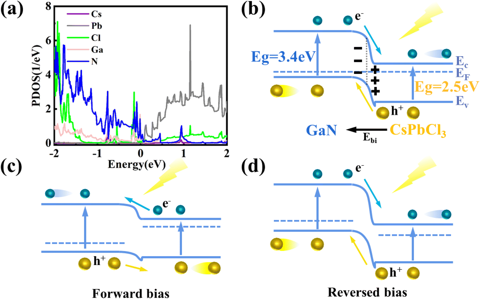
In order to study the substrate quality and optical characteristics, the p-GaN substrate was characterized by PL and XRD. Fig. S1(a)† shows the rocking curves of the (002) and (102) planes, which are consistent with previous reports38,39 after normalization, indicating the high quality of the used substrate. To obtain the macroscopic orientation of p-GaN, the substrate was scanned by ω-2θ XRD. According to the ω-2θ XRD scan shown in Fig. S1(b),† the crystal plane orientation of GaN is (002), while the rest of the peaks are caused by sapphire. As shown in Fig. S1(c),† the characteristic peak of the PL spectrum is at about 365 nm, indicating that the band gap value of the used p-GaN substrate is about 3.4 eV, which is consistent with previous reports.40Besides, the surface morphology of CsPbCl3 spin-coated on the GaN substrate is tested, as shown in Fig. S2.† Fig. S2(a)† shows the SEM image of the sample. From the image, it can be seen that the surface of CsPbCl3 prepared by the spin coating method is relatively flat and forms a continuous large-area crystal with a size of several hundred microns. Large-area uniform CsPbCl3 nanocrystals are not only convenient for device preparation, but also conducive to improving device performance. In addition, it can be observed that there is a certain gap between CsPbCl3 films, which is determined by the surface roughness of the substrate. The rougher the substrate surface, the stronger the bond between CsPbCl3 and the substrate, but the larger the gap between CsPbCl3 nanocrystals, which will affect the device performance. At the same time, in order to further observe the microstructure and transfer quality of CsPbCl3 nanocrystals, the samples were analyzed by TEM, as shown in Fig. S2(b).† It can be seen from the figure that CsPbCl3 nanocrystals have good monodispersity and uniform distribution of quantum dots.
In addition, through further TEM analysis in Fig. 2(a), it is not difficult to find that the stripe of CsPbCl3 is clear, and the lattice type is a cubic lattice, which matches the previous report.41 Subsequently, the ω-2θ XRD scan of CsPbCl3 nanocrystals shows that their diffraction peaks can be well matched with the previously reported diffraction peaks (100), (101), (200), (201) and (220) of CsPbCl3,20,42 while a small number of redundant diffraction peaks are attributed to the influence of the p-GaN substrate, as shown in Fig. 2(d).43,44 Meanwhile, energy dispersive spectroscopy (EDS) analysis of the sample was performed to determine the element composition and distribution of the sample, as shown in Fig. 4(c), (e) and (f). By comparing the EDS mapping diagram of each element with the light microscope diagram of EDS scanning area in Fig. 2(b), different element distribution diagrams show that each element is evenly distributed and the quality of nanocrystalline formation is good. From the figure, the distribution density of Cs and Pb elements is similar, while the distribution of Cl is the densest, which is about 1![[thin space (1/6-em)]](https://www.rsc.org/images/entities/char_2009.gif) :1:3. According to the TEM images, it is further verified that the spin-coating is cubic lattice CsPbCl3 nanocrystals.
:1:3. According to the TEM images, it is further verified that the spin-coating is cubic lattice CsPbCl3 nanocrystals.
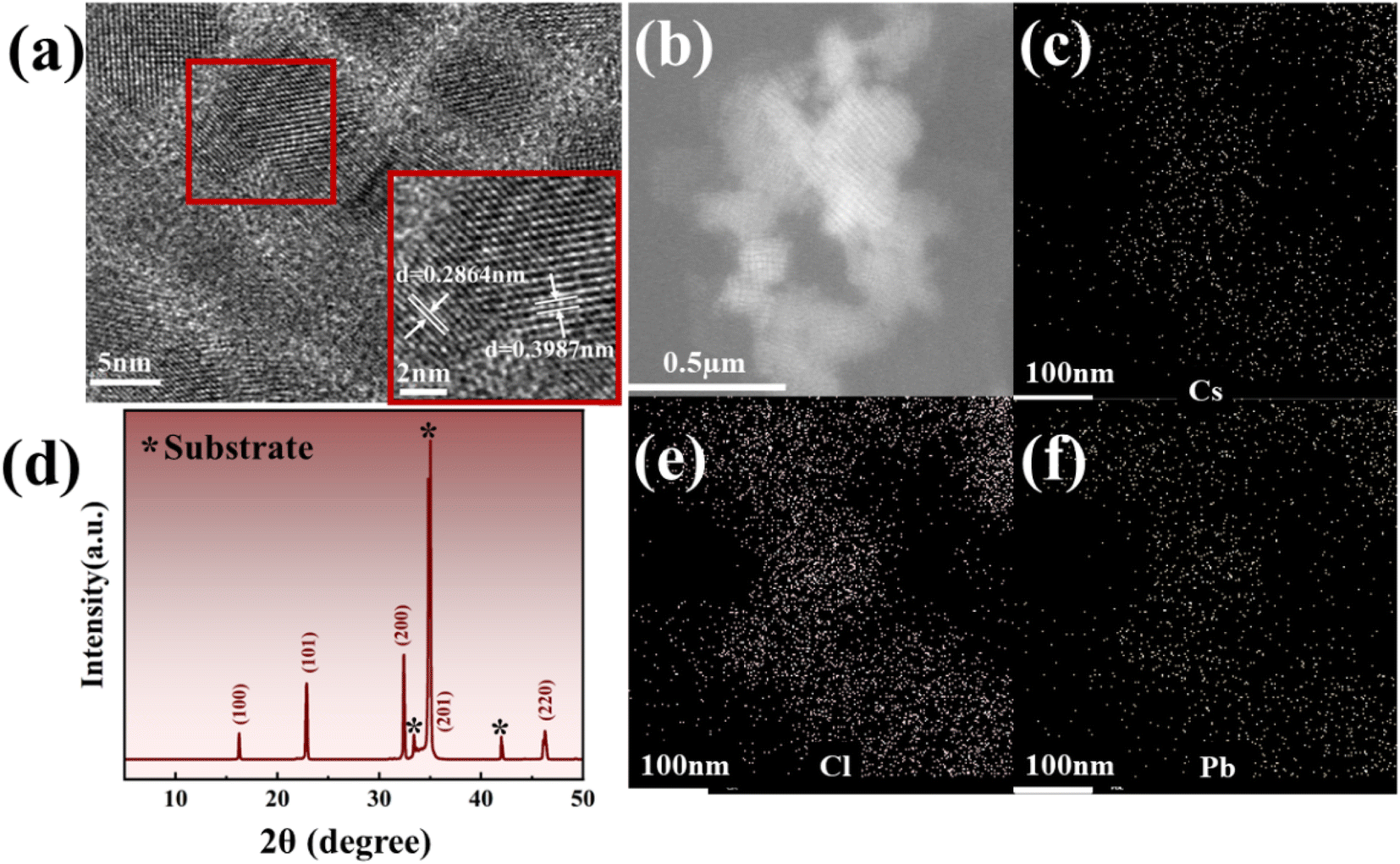 | ||
| Fig. 2 (a) TEM analysis image of CsPbCl3; (b) EDS scanning area; (c), (e) and (f) EDS mapping images of each element of CsPbCl3; (d) ω-2θ XRD scan of CsPbCl3. | ||
In order to obtain the optical properties of CsPbCl3 nanocrystals for the subsequent research and analysis of photoelectric characteristics of devices, PL and absorption spectra were obtained. Fig. S3(a)† shows the PL spectrum of CsPbCl3 nanocrystals, and the characteristic peak is at 420 nm, which is mainly caused by the exciton emission of the CsPbCl3 band. It can be seen from Fig. S3(b)† that the absorption spectrum peak position of CsPbCl3 nanocrystals is at around 420 nm, which is consistent with the PL peak position. Combining the PL characteristic peak with the absorption peak, the band gap value of CsPbCl3 nanocrystals prepared in this experiment is about 2.95 eV.
One of the most important reasons why all-inorganic perovskite has attracted extensive research and attention is its excellent optical properties in the visible–ultraviolet region and adjustable band gap. The schematic diagram of the CsPbCl3/GaN heterojunction device is shown in Fig. 3(a). Ni/Au was evaporated on CsPbCl3 and the GaN substrate to form metal electrodes, respectively. At room temperature, the dark current of the device was tested first, and the applied voltage was −2 V to 2 V. It can be seen that the device has a dark current as low as 2.42 × 10⁻⁹ A at 1 V. Meanwhile, the device shows obvious rectification behavior, which can be attributed to the presence of the CsPbCl3/GaN heterojunction. Subsequently, I–V characteristics of the device were tested under 365 nm and 420 nm illumination, respectively, and the results are shown using the red line and blue line in Fig. 3(b), respectively. The incident light power density used in this experiment was 1.76 μW mm−2. As can be seen from the figure, no matter under the forward bias voltage or the reverse bias voltage, there are obvious photoresponse behaviors under the illumination conditions of 365 nm and 420 nm when compared under dark conditions. As mentioned above, the PL spectral characteristic peaks of GaN and CsPbCl3 are close to 365 nm and 420 nm, for which photons of the wavelength can provide enough energy to make carriers transition to form photocurrent. Responsivity is an important device parameter of a photodetector, which can intuitively show the photoelectric conversion capability of the device. It can be expressed by using the following formula: R = Iph/Pin, where Iph represents the net photocurrent and Pin represents the incident light power. In order to further study the photoresponse behavior of the CsPbCl3/GaN heterojunction at different bias voltages, the responsivity of the device was measured in the range of 300–500 nm at bias voltages of −2 V, −1 V and 1 V respectively, as shown in Fig. 3(c). It can be seen from the figure that the device has obvious broadband photoresponse behavior at both positive and negative bias voltages. The difference is that there is a sudden dip at 365 nm at a positive bias voltage and no such dip at a negative bias voltage. In addition, the detectivity corresponding to the responsivity is calculated by using the formula D* = R/(2qId/A)1/2, which represents the capability of the device to detect weak optical signals. Among them, R is the responsivity, q represents the electron charge, Id represents the dark current, and A is the effective area of the photodetector. At −2 V bias, the responsivity of the device at 365 nm and 420 nm is 15.7 mA W−1 and 15.0 mA W−1, respectively, and the corresponding detectivity is 2.58 × 10¹⁰ Jones and 2.47 × 10¹⁰ Jones, respectively. Finally, the device is subjected to continuous switching modulation to test the response speed of the device. Fig. S4(a) and (b)† show the continuous switching modulation curves of the device under 365 nm and 420 nm light respectively, and the modulation period is 40 seconds. The rise/fall time of the device is 0.56 s/0.52 s, respectively.
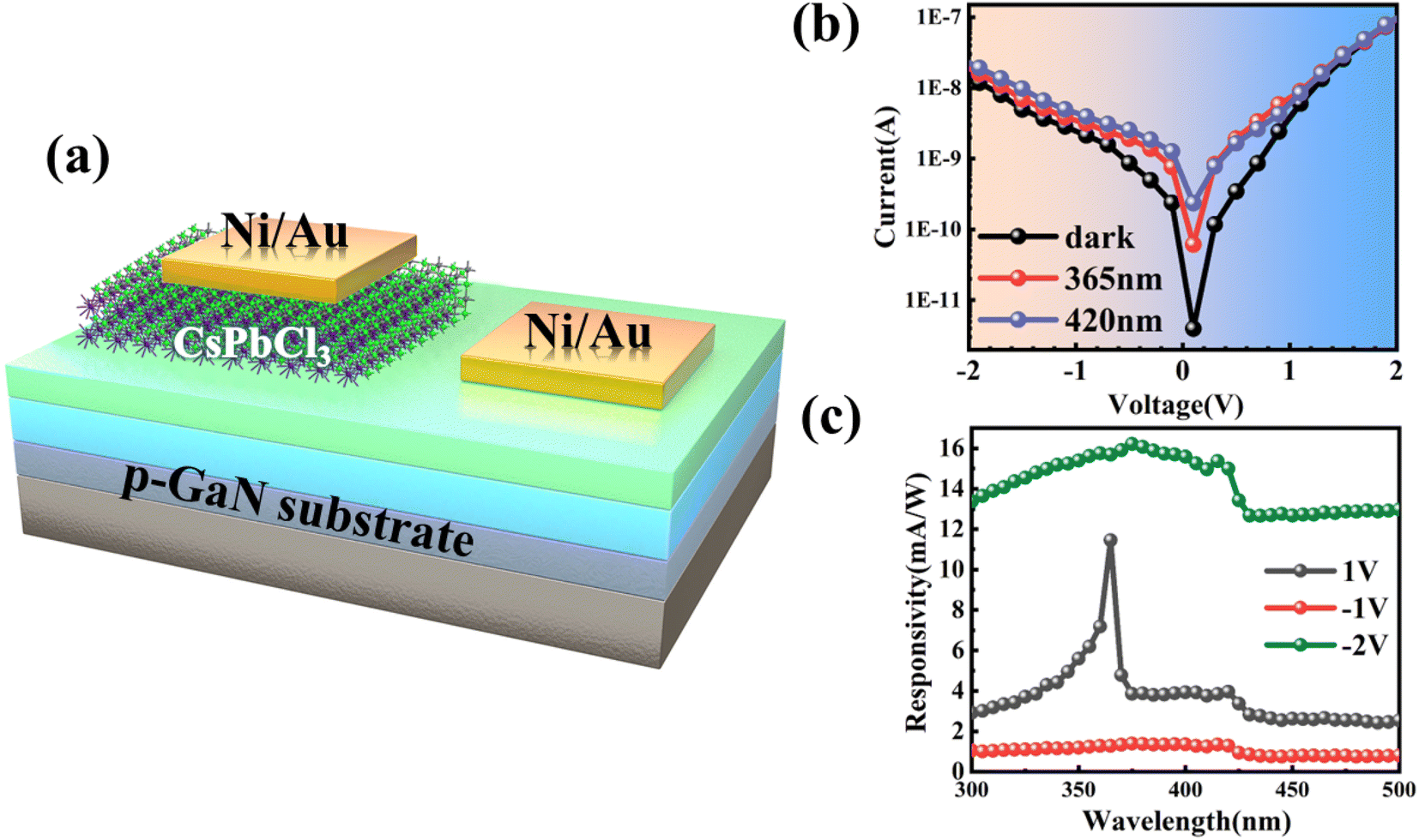 | ||
| Fig. 3 (a) Schematic diagram of the CsPbCl3/GaN heterojunction photodetector; (b) I–V characteristic curves of the device under dark conditions, 365 nm illumination and 420 nm illumination; (c) photoresponse of devices in the visible–ultraviolet range at bias voltages of 1 V, −1 V and −2 V. | ||
To further study the electrical and photoelectric properties of CsPbCl3, GaN and the layered CsPbCl3/GaN heterojunction, and deeply analyze the mechanism of the heterojunction, the first-principles calculation of heterojunction materials was carried out in this experiment. First, model and calculate the energy band of isolated materials. The energy band diagram of CsPbCl3 is shown in Fig. S5(a)†. From the diagram, it can be concluded that CsPbCl3 has a band gap value of 2.5 eV and is a direct band gap semiconductor, of which both the CBM and VBM are at the L point. Although the theoretical band gap value is less than the experimental value of 2.95 eV, the GGA-PBE calculation method usually underestimates the band gap value, which has not affected the subsequent simulation calculation. Besides, compared with the related literature,45 the simulation value of this work is closer to the experimental value than that in the previous work, which shows that the simulation result is reliable. At the same time, the energy band diagram of GaN in Fig. S5(b)† shows that the simulated GaN is a direct bandgap semiconductor with both the CBM and VBM at the G point, which is highly consistent with the experimentally obtained 3.4 eV bandgap value. After optimization, the lattice constants of CsPbCl3 and GaN are 5.751 Å and 3.180 Å, respectively, which match those in the previous work.46,47
After verifying the reliability of the materials, the heterojunction of the two materials is built and optimized, as shown in Fig. 4(a) and (b). In the process of optimization, the minimum stress between heterojunction atoms is set, resulting in a change in the atom position at the interface of the heterojunction. The convergence of optimization results shows that the heterojunction has a stable structure. Fig. 4(c) shows a schematic diagram of the projected energy band of the heterojunction, in which the red line represents CsPbCl3 while the blue line stands for GaN. The thickness in the figure represents the weight of the material in the energy band. Compared with Fig. S5,† the heterojunction energy band structure in Fig. 4(c) is modulated. In order to further analyze the band structure types of the CsPbCl3/GaN heterojunction, the projected density of states (PDOS) of the heterojunction is calculated, and the result is shown in Fig. 5(a). Obviously, the CsPbCl3/GaN heterojunction has a type II energy band arrangement, in which the valence band is mainly contributed by N atoms in GaN, while the conduction band is dominated by Pb atoms in CsPbCl3.
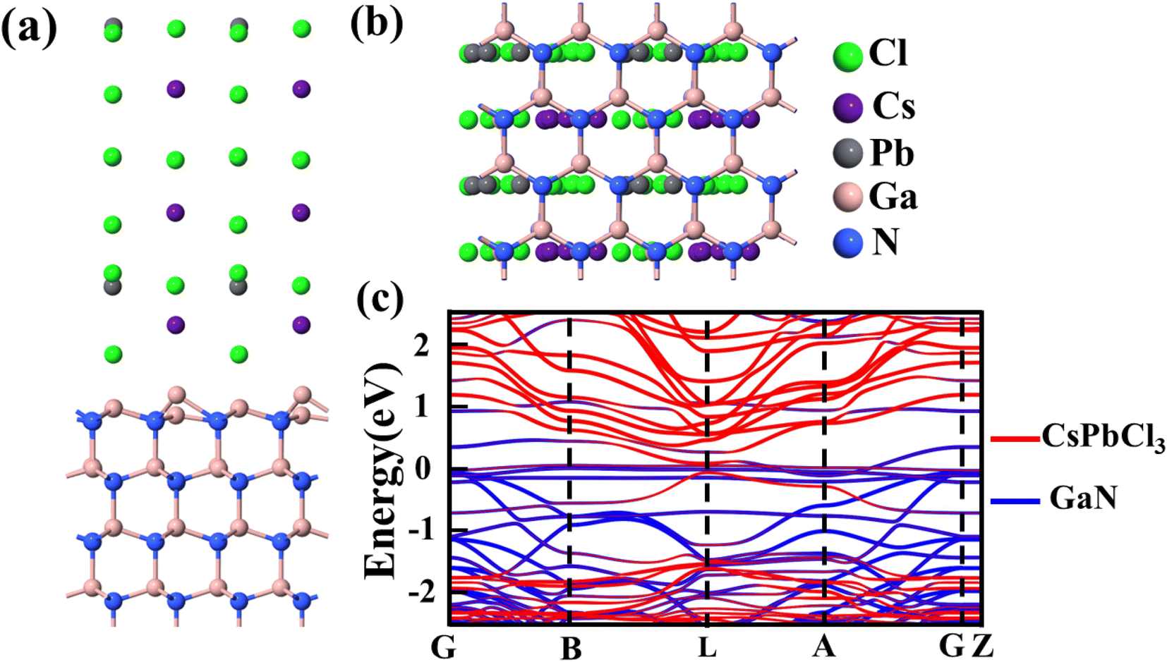 | ||
| Fig. 4 (a) Side view; (b) top view; (c) projected energy band diagram of the CsPbCl3/GaN heterojunction. | ||
 | ||
| Fig. 5 (a) PDOS of the CsPbCl3/GaN heterojunction; (b) schematic diagram of the energy band profile of the CsPbCl3/GaN heterojunction; schematic diagram of the energy band profile under (c) forward bias and (d) reversed bias. | ||
According to the energy band structure diagram and PDOS of the heterojunction, the schematic diagram of the CsPbCl3/GaN heterojunction energy band profile in Fig. 5(b) is obtained. Based on the previous report, CsPbCl3 is considered as an n-type semiconductor in the drawn heterojunction band profile.48 When CsPbCl3 is in contact with GaN, the Fermi energy level reaches an equilibrium state, and there are different barrier heights between the conduction band and the valence band. Fig. S6(a)† shows the electron localization function of the CsPbCl3/GaN heterojunction, which shows the strong electron localization of the heterojunction, indicating that the structure is stable.
In addition to electrical properties, the optical properties of the CsPbCl3/GaN heterojunction are also remarkable. In order to compare the differences in optical properties before and after the formation of a heterojunction, the photon energy-related optical absorption coefficients of isolated GaN, CsPbCl3 and the CsPbCl3/GaN heterojunction are calculated respectively. As shown in Fig. S6(b),† isolated GaN and CsPbCl3 have strong absorption of photons in the near ultraviolet and ultraviolet regions, but weak absorption of photons in the visible region. After the formation of a heterostructure, the absorption of the CsPbCl3/GaN heterostructure in the visible region is greatly increased, and there is still some absorption in the near ultraviolet region. The enhancement of light absorption in the visible region and near ultraviolet region will be beneficial to the photoelectric performance of CsPbCl3/GaN heterojunction devices, since their band gaps correspond to photon energy in visible and near ultraviolet regions, respectively. The stronger light absorption in corresponding bands will be beneficial to the collection of photons and the formation of photocurrent.
Finally, the photoresponse behavior of the device is explained in connection with the drawn energy band profiles in Fig. 5(c) and (d). Combined with the energy band diagram in Fig. 5(b), when the two materials are in contact, CsPbCl3 electrons flow to GaN until the Fermi level is equal. As a result, a built-in electric field is formed, whose direction is from CsPbCl3 to GaN. When a forward bias is applied, the potential barrier decreases since the direction of the voltage is opposite to the direction of the built-in electric field. At the same time, the Fermi level of the heterojunction deviates from the equilibrium position because of the change in the potential barrier.49,50 When 365 nm and 420 nm wavelengths of light are used, the photon energy is sufficient to separate electron–hole pairs on GaN and CsPbCl3. Due to the reduction of the potential barrier, the carriers have the ability to cross the potential barrier to form photocurrent. It can be seen from the energy band profile diagram that the barrier height of the valence band is smaller and lower than that of the conduction band, so the photogenerated carriers at GaN are more likely to cross the barrier to form photocurrent. When a reverse bias is applied, the photogenerated carriers have no potential barrier, forming a photoresponse curve as shown in Fig. 3(c). At the forward bias, due to the presence of the potential barrier, the photogenerated carriers on the CsPbCl3 side are severely blocked, while the band gap value of GaN only allows photons with an energy greater than 3.4 eV to pass through. As a result, the photocurrent after 365 nm decreases sharply. Under reverse bias, the photogenerated carriers of CsPbCl3 and GaN can smoothly reach both ends of the electrode to form a photocurrent due to the absence of a potential barrier. However, the photocurrent of CsPbCl3 after 365 nm is larger, resulting in no obvious sudden drop observed at 365 nm. Overall, CsPbCl3/p-GaN heterojunction photodetectors have successfully achieved visible–ultraviolet dual-band response no matter in forward bias or reverse bias.
Table 1 shows the performance comparison of our CsPbCl3/p-GaN heterostructure dual-band photodetector with other different MHP photodetectors. It can be seen that the performance of photodetectors based on the CsPbCl3/p-GaN heterojunction is comparable to that of other devices, and especially the response wavelength range is better than that of other MHP photodetectors.
| Materials | Dark current (A) | Responsivity (mA W−1) | Detectivity (Jones) | Wavelength (nm) | Rise time/fall time | Reference |
|---|---|---|---|---|---|---|
| CsPbCl3/GaN | 2.42 × 10⁻⁹ (1 V) | 11.5 (365 nm 1 V) | 5.82 × 10¹⁰ | 300–420 | 0.56 s/0.52 s | This work |
| 4.0 (420 nm 1 V) | 2.58 × 10¹⁰ | |||||
| 2.31 × 10⁻⁸ (−2 V) | 15.7 (365 nm to 2 V) | 2.01 × 10¹⁰ | ||||
| 15.0 (420 nm to 2 V) | 2.47 × 10¹⁰ | |||||
| CsPbCl3 microwire networks | 1 × 10⁻¹⁰ (10 V) | 14.3 (405 nm 10 V) | — | 325–420 | 20.9 ms/24.6 ms | 51 |
| Dual-phase CsPbCl3–Cs4PbCl6 films | 9.8 × 10⁻⁷ (−0.5 V) | 61.8 (405 nm 0 V) | 1.35 × 10¹² | 310–420 | 2.1 μs/5.3 μs | 20 |
| CsPbBr3 | 7.98 × 10⁻⁸ (5 V) | 28 (450 nm 5 V) | 1.8 × 10¹¹ | 450 | 90.7 ms/57 ms | 52 |
| (HDA)CsPb2Br7 | 2.34 × 10⁻¹¹ (10 V) | 0.21 (405 nm) | 1.5 × 10⁹ | 405 | 200 μs/300 μs | 53 |
| (2meptH2)CsPb2Br7 | 1.7 × 10⁻¹¹ (10 V) | 100 (266 nm 10 V) | 1 × 10⁹ | 266, 377 | 232 μs/150 μs | 54 |
| CsPbBr3 | 5 × 10⁻¹⁰ (2 V) | 10.04 (532 nm 2 V) | 4.56 × 10⁸ | 532 | 0.2 ms/1.2 ms | 55 |
| CsPbCl3 single crystal | 9 × 10⁻¹⁰ (5 V) | 4.52 (365 nm 5 V) | 3.3 × 10¹⁰ | 365 | 104 ms | 56 |
| Tetragonal phase CsPbCl3 single crystal | 1.3 × 10⁻⁷ (1 V) | 268 (360 nm 1 V) | 1.588 × 10¹⁰ | 280–435 | 28.4 ms/2.7 ms | 45 |
| ZnO/CsPbCl3 nanowires | 8.3 × 10⁻¹¹ (1 V) | 4 × 10³ (380 nm 1 V) | 1.71 × 10⁹ | 380, 760 | 0.42 s/0.63 s | 57 |
| CH3NH3PbCl3 single crystal | 4.15 × 10⁻⁷ (15 V) | 46.9 (365 nm 15 V) | 1.2 × 10¹⁰ | 365 | 24 ms/62 ms | 58 |
| CH3NH3PbCl3 single crystal | 3 × 10⁻⁸ (10 V) | 0.62 (405 nm 10 V) | 5.5 × 10⁹ | 405 | — | 59 |
Conclusion
In summary, the CsPbCl3/p-GaN heterojunction was successfully fabricated by the spin-coating method and used for photodetection. Subsequent XRD, SEM, and EDS mapping proved the successful formation of the heterojunction. From the combination of PL, absorption spectrum and photoelectric test results, it can be known that the dual response bands of the heterojunction correspond to the response bands of CsPbCl3 and GaN. At the same time, the device has obvious photoresponse behavior at small forward and reverse bias voltages. Through the simulation calculation of the heterojunction, it is found that the formation of the heterojunction not only makes the two materials form a type II energy band alignment and effectively separates the electron–hole pairs, but also enhances the light absorption of the material. The successful realization of visible–ultraviolet dual-band photodetectors based on the CsPbCl3/p-GaN heterojunction provides guidance for the application of all-inorganic MHPs in the field of multi-band photodetectors.Conflicts of interest
The authors declare no competing financial interest.Acknowledgements
This work was funded by the National Natural Science Foundation of China (No. 62374075, 61974056, 62375028, 62174016, 62074019, and 32241010), the Key Research and Development Program of Jiangsu Province (No. BE2020756), the Natural Science Foundation of Jiangsu Province (No. BK20190576), the Suzhou Science and Technology Project (No. SZS2020313), the Anhui Provincial Natural Science Foundation (2308085MF205), and the Fundamental Research Funds for Central Universities (No. JUSRP22032).Notes and references
- D. Bi, C. Yi, J. Luo, J. Décoppet, F. Zhang, S. M. Zakeeruddin, X. Li, A. Hagfeldt and M. Grätzel, Nat. Energy, 2016, 1, 16142 CrossRef CAS.
- D. B. Khadka, Y. Shirai, M. Yanagida and K. Miyano, J. Mater. Chem. C, 2019, 7, 8335–8343 RSC.
- J. Zheng, M. Zhang, C. Lau, X. Deng, J. Kim, Q. Ma, C. Chen, M. A. Green, S. Huang and A. Ho-Baillie, Sol. Energy Mater. Sol. Cells, 2017, 168, 165–171 CrossRef CAS.
- R. S. Brandon and H. S. Edward, Nat. Photonics, 2016, 10, 295–302 CrossRef.
- N. Wang, L. Cheng, J. Si, X. Liang, Y. Jin, J. Wang and W. Huang, Appl. Phys. Lett., 2016, 108, 141102 CrossRef.
- H. Cho, S. Jeong, M. Park, Y. Kim, W. Christoph, C. Lee, J. H. Heo, S. Aditya, N. Myoung, S. Yoo, S. H. Im, F. Richard H and T. Lee, Science, 2015, 350, 1222–1225 CrossRef CAS PubMed.
- V. Adinolfi, O. Ouellette, M. I. Saidaminov, G. Walters, A. L. Abdelhady, O. M. Bakr and E. H. Sargent, Adv. Mater., 2016, 28, 7264–7268 CrossRef CAS PubMed.
- J. Ding, H. Fang, Z. Lian, J. Li, Q. Lv, L. Wang, J. Sun and Q. Yan, CrystEngComm, 2016, 18, 4405–4411 RSC.
- J. Yu, X. Chen, Y. Wang, H. Zhou, M. Xue, Y. Xu, Z. Li, C. Ye, J. Zhang and P. van Aken, J. Mater. Chem. C, 2016, 4, 7302–7308 RSC.
- M. Kulbak, D. Cahen and G. Hodes, J. Phys. Chem. Lett., 2015, 6, 2452–2456 CrossRef CAS PubMed.
- C. Li, Z. Zang, W. Chen, Z. Hu, X. Tang, W. Hu, K. Sun, X. Liu and W. Chen, Opt. Express, 2016, 24, 15071–15078 CrossRef CAS PubMed.
- X. Tang, Z. Hu, W. Chen, X. Xing, Z. Zang, W. Hu, J. Qiu, J. Du, Y. Leng and X. Jiang, Nano Energy, 2016, 28, 462–468 CrossRef CAS.
- J. Song, L. Xu, J. Li, J. Xue, Y. Dong, X. Li and H. Zeng, Adv. Mater., 2016, 28, 4861–4869 CrossRef CAS PubMed.
- M. Kovalenko, L. Protesescu and M. Bodnarchuk, Science, 2017, 358, 745–750 CrossRef CAS PubMed.
- Q. Akkerman, G. Rainò, M. Kovalenko and L. Manna, Nat. Mater., 2018, 17, 394–405 CrossRef CAS PubMed.
- L. Protesescu, S. Yakunin, M. Bodnarchuk, F. Krieg, R. Caputo, C. Hendon, R. Yang, A. Walsh and M. Kovalenko, Nano Lett., 2015, 15, 3692–3696 CrossRef CAS PubMed.
- D. Hofstetter, R. Theron, E. Baumann, F. R. Giorgetta, S. Golka, G. Strasser, F. Guillot and E. Monroy, Electron. Lett., 2009, 44, 986–988 CrossRef.
- M. Dai, H. Chen, R. Feng, W. Feng, Y. Hu, H. Yang, G. Liu, X. Chen, J. Zhang and C. Xu, ACS Nano, 2018, 12, 8739–8747 CrossRef CAS PubMed.
- J. Shao, A. Perera, P. Jayaweera and D. He, Chin. Phys. Lett., 2010, 27, 027302 CrossRef.
- W. Zhu, M. Deng, D. Chen, Z. Zhang, W. Chai, D. Chen, H. Xi, J. Zhang, C. Zhang and Y. Hao, ACS Appl. Mater. Interfaces, 2020, 12, 32961–32969 CrossRef CAS PubMed.
- L. Hu, J. Yan, M. Liao, H. Xiang, X. Gong, L. Zhang and X. Fang, Adv. Mater., 2012, 24, 2305–2309 CrossRef CAS PubMed.
- S. Tong, J. Sun, C. Wang, Y. Huang, C. Zhang, J. Shen, H. Xie, D. Niu, S. Xiao and Y. Yuan, Adv. Electron. Mater., 2017, 3, 1700058 CrossRef.
- J. Ma, X. Xia, S. Yan, Y. Li, W. Liang, J. Yan, X. Chen, D. Wu, X. Li and Z. Shi, ACS Appl. Mater. Interfaces, 2021, 13, 15409–15419 CrossRef CAS PubMed.
- Y. Li, Z. Shi, W. Liang, L. Wang, S. Li, F. Zhang, Z. Ma, Y. Wang, Y. Tian, D. Wu, X. Li, Y. Zhang, C. Shan and X. Fang, Mater. Horiz., 2020, 7, 530–540 RSC.
- W. Liang, Z. Shi, Y. Li, J. Ma, S. Yin, X. Chen, D. Wu, Y. Tian, Y. Tian, Y. Zhang, X. Li and C. Shan, ACS Appl. Mater. Interfaces, 2020, 12, 37363–37374 CrossRef CAS PubMed.
- H. Algadi, C. Mahata, J. Woo, M. Lee, M. Kim and T. Lee, Electronics, 2019, 8, 678 CrossRef CAS.
- J. Lu, M. Zhang, J. Yao, Z. Zheng, L. Tao, Y. Zhao and J. Li, ACS Appl. Nano Mater., 2021, 4, 5106–5114 CrossRef CAS.
- J. Zhang, Q. Wang, X. Zhang, J. Jiang, Z. Gao, Z. Jin and S. Liu, RSC Adv., 2017, 7, 36722–36727 RSC.
- X. Zhan, X. Zhang, Z. Liu, C. Chen, L. Kong, S. Jiang, S. Xi, G. Liao and X. Liu, ACS Appl. Mater. Interfaces, 2021, 13, 45744–45757 CrossRef CAS PubMed.
- A. Gundimeda, S. Krishna, N. Aggarwal, A. Sharma, N. D. Sharma, K. K. Maurya, S. Husale and G. Gupta, Appl. Phys. Lett., 2017, 110, 103507 CrossRef.
- X. Zhou, C. Wang, J. Luo, L. Zhang, F. Zhao and Q. Ke, Chem. Eng. J., 2022, 450, 136364 CrossRef CAS.
- Y. Huang, L. Zhang, J. Wang, X. Chu, D. Zhang, X. Zhao, X. Li, L. Xin, Y. Zhao and F. Zhao, J. Alloys Compd., 2019, 802, 70–75 CrossRef CAS.
- R. Zhuo, L. Zeng, H. Yuan, D. Wu, Y. Wang, Z. Shi, T. Xu, Y. Tian, X. Li and Y. Tsang, Nano Res., 2019, 12, 183–189 CrossRef CAS.
- S. Solanke, R. Soman, M. Rangarajan, S. Raghavan and D. Nath, Sens. Actuators, A, 2021, 317, 112455 CrossRef CAS.
- E. Fortunati, S. Mattioli, I. Armentano and J. Kenny, Carbohydr. Polym., 2014, 113, 394–402 CrossRef CAS PubMed.
- R. Nisticò, D. Scalarone and G. Magnacca, Microporous Mesoporous Mater., 2017, 248, 18–29 CrossRef.
- M. J. van Setten, M. Giantomassi, E. Bousquet, M. J. Verstraete, D. R. Hamann, X. Gonze and G. M. Rignanese, Comput. Phys. Commun., 2018, 226, 39–54 CrossRef CAS.
- K. Wang, M. Li, Z. Yang, J. Wu and T. Yu, CrystEngComm, 2019, 21, 4792–4797 RSC.
- Y. Chen, Z. Chen, J. Li, Y. Chen, C. Li, J. Zhan, T. Yu, X. Kang, F. Jiao and S. Li, CrystEngComm, 2018, 20, 6811–6820 RSC.
- K. Zhang, B. Jariwala, J. Li, N. C. Briggs, B. Wang, D. Ruzmetov, R. A. Burke, J. O. Lerach, T. G. Ivanov, M. Haque, R. M. Feenstra and J. A. Robinson, Nanoscale, 2018, 10, 336 RSC.
- M. Gong, R. Sakidja, R. Goul, D. Ewing, M. Casper, A. Stramel, A. Elliot and J. Z. Wu, ACS Nano, 2019, 13, 1772–1783 CrossRef CAS PubMed.
- Z. Zhu, W. Deng, W. Li, F. Chun, C. Luo, M. Xie, B. Pu, N. Lin, B. Gao and W. Yang, Adv. Mater. Interfaces, 2021, 8, 2001812 CrossRef CAS.
- S. Mitra, M. Muhammed and N. Alwadai, RSC Adv., 2020, 10, 6092–6097 RSC.
- X. Liu, D. Cao, Y. Yao, P. Tang, M. Zhang, X. Chen and H. Shu, J. Mater. Chem. C, 2022, 10, 1984–1990 RSC.
- Z. Rao, W. Liang, H. Huang, J. Ge, W. Wang and S. Pan, Opt. Mater. Express, 2020, 10, 1374–1382 CrossRef CAS.
- Y. Li, Q. Liu, X. Liu, J. Feng, L. He, H. Li, C. Li and H. Zhang, J. Phys. Chem. Lett., 2021, 12, 10746–10752 CrossRef CAS PubMed.
- S. K. Jain, M. X. Low, P. D. Taylor, S. A. Tawfik, M. J. Spencer, S. Kuriakose, A. Arash, C. Xu, S. Sriram, G. Gupta, M. Bhaskaran and S. Walia, ACS Appl. Electron. Mater., 2021, 3, 2407–2414 CrossRef CAS.
- Y. Zhang, X. Cheng, D. Tu, Z. Gong, R. Li, Y. Yang, W. Zheng, J. Xu, S. Deng and X. Chen, Angew. Chem., Int. Ed., 2021, 60, 9693–9698 CrossRef CAS PubMed.
- Q. Lv, F. Yan, X. Wei and K. Wang, Adv. Opt. Mater., 2018, 6, 1700490 CrossRef.
- X. Wei, F. Yan, Q. Lv, C. Shen and K. Wang, Nanoscale, 2017, 9, 8388–8392 RSC.
- Y. Li, Z. Shi, L. Lei, Z. Ma, F. Zhang, S. Li, D. Wu, T. Xu, X. Li and C. Shan, ACS Photonics, 2018, 5, 2524–2532 CrossRef CAS.
- J. Ding, S. Du, Z. Zuo, Y. Zhao, H. Cui and X. Zhan, J. Phys. Chem. C, 2017, 121, 4917–4923 CrossRef CAS.
- T. Yang, Y. Li, S. Han, Z. Xu, Y. Liu, X. Zhang, X. Liu, B. Teng, J. Luo and Z. Sun, Small, 2020, 16, 1907020 CrossRef CAS PubMed.
- D. Fu, S. Wu, J. Xin, X. Zhang, G. Han and X. Zhang, Chem. Commun., 2020, 56, 14381–14384 RSC.
- Y. Dong, Y. Gu, Y. Zou, J. Song, L. Xu, J. Li, F. Xue, X. Li and H. Zeng, Small, 2016, 12, 5622–5632 CrossRef CAS PubMed.
- Q. Wang, Z. Gong, S. Wu, S. Pan and J. Pan, J. Cryst. Growth, 2022, 596, 126838 CrossRef CAS.
- T. Gao, Q. Zhang, J. Chen, X. Xiong and T. Zhai, Adv. Opt. Mater., 2017, 5, 1700206 CrossRef.
- G. Maculan, A. D. Sheikh, A. L. Abdelhady, M. I. Saidaminov, M. A. Haque, B. Murali, E. Alarousu, O. F. Mohammed, T. Wu and O. M. Bakr, J. Phys. Chem. Lett., 2015, 6, 3781–3786 CrossRef CAS PubMed.
- X. Cheng, L. Jing, Y. Zhao, S. Du, J. Ding and T. Zhou, J. Mater. Chem. C, 2018, 6, 1579–1586 RSC.
Footnote |
| † Electronic supplementary information (ESI) available: Rocking curve, ω-2θ XRD scanning of the (002) plane and the PL spectrum of the GaN substrate; SEM images and TEM images of CsPbCl3 nanocrystals; PL spectrum and absorption spectrum of the CsPbCl3 nanocrystal; continuous switching modulation curves of devices under 350 nm and 420 nm illumination, with a period of 40 s; energy band diagram of CsPbCl3 and energy band diagram of GaN. See DOI: https://doi.org/10.1039/d3na01009k |
| This journal is © The Royal Society of Chemistry 2024 |