DOI:
10.1039/D3NA00905J
(Paper)
Nanoscale Adv., 2024,
6, 680-689
Optical and thermoelectric properties of new Janus ZnMN2 (M = Ge, Sn, Si and N = S, Se, Te) monolayers: a first-principles study
Received
20th October 2023
, Accepted 26th November 2023
First published on 5th December 2023
Abstract
Thermoelectric materials have received great interest because they directly tap into the vast reserves of currently underused thermal energy, in an environmentally friendly manner. In this work, we investigated the electronic, optical and thermoelectric properties of novel ZnMN2 (M = Ge, Sn, Si and N = S, Se, Te) monolayers by performing density functional theory calculations. The dynamic and thermal stabilities of ZnMN2 (M = Ge, Sn, Si and N = S, Se, Te) monolayers were confirmed by their phonon band structures and ab initio molecular dynamics (AIMD) simulations, which showed that all the studied monolayers are stable. Calculated electronic band structures showed that ZnSiTe2, ZnGeSe2, and ZnSnTe2 have a direct band gap, while the remaining monolayers have an indirect band gap. Optical properties in terms of the imaginary part of the dielectric function have also been investigated, which showed that all the first excitonic peaks lie in the visible region. Transport coefficients, such as the Seebeck coefficient (S), electrical conductivity (σ) and power factor (PF) were calculated using the Boltzmann theory and plotted against chemical potential. The results demonstrated that the peak values of the p-type region for the PF are greater than those of the n-type region. Notably, ZnSiTe2 exhibits a large PF due to its smaller Seebeck coefficient and higher electrical conductivity compared to ZnSnS2, indicating that it is a promising candidate for thermoelectric applications. Our findings reveal that ZnMN2 (M = Ge, Sn, Si and N = S, Se, Te) monolayers open up new possibilities for optoelectronics and thermoelectric device applications.
I. Introduction
A shortage of energy is currently predicted to be a great challenge in the near future for our society.1 It is expected that the world’s energy demands will rise by up to 60% by 2030.1 Currently, about 80% of the world’s energy is generated by heat engines using fossil fuels as an energy source, which has a big drawback of carbon dioxide emission.1 Due to this increasing demand for clean energy, researchers are trying to develop renewable energy sources to resolve energy issues and also to avoid environmental pollution.2,3 Recently, solar cells, wind-driven generators, thermoelectric devices and fuel cells have attracted tremendous attention. Among these resources, thermoelectric devices have gained much attention due to their many applications, including cooling devices, sensors and power generators.4–7 Thermoelectric materials have the ability to directly convert thermal energy, such as solar and waste energy, to electrical energy, which makes them suitable for development into sustainable energy devices.8–10 In comparison with other energy sources, thermoelectric devices have advantages of stability, silent operation and long service life.11–13 The efficiency of thermoelectric materials depends on the Seebeck coefficient (S), electrical conductivity (σ), total conductivity (K) and absolute temperature (T). For efficient thermoelectric materials, the electrical conductivity (σ) and Seebeck coefficient (S) is high and the thermal conductivity is low.14,15
Since the discovery of single-layer graphene in 2004,16 research interest in the field of 2D materials has grown explosively in just a few years. Recently, thanks to developments in synthesis techniques and theoretical simulation, a variety of 2D materials have been theoretically predicted and successfully fabricated, such as hexagonal boron nitride (h-BN),17 transition-metal dichalcogenides (TMDCs),18 group-III metal chalcogenides,20 group-IV and -VI metal monochalcogenides, such as SiO, SiS, GeS and SnS,21 and carbide and nitride semiconductors.22 Lately, a novel class of 2D materials named Janus transition-metal dichalcogenides (JTMDCs) has attracted attention from researchers due to the distinct properties that the materials obtain from their parent transition-metal dichalcogenide monolayers. Lu and co-workers23 confirmed the successful fabrication of JTMDCs by using chemical vapor deposition (CVD). Recently, a group of novel 2D Janus group-III monochalcogenides with the general formula ZnXY2 (X = Si, Ge, Sn and Y = S, Se, Te) and constructed according to their isoelectronic mutation has been investigated, and refers to group-III monochalcogenides,24 which have been attracting much interest due to their higher piezoelectricity, direct band-gaps and large effective mass difference, making them good candidates for applications in optoelectronics, photocatalysis, flexible nanodevices and electromechanical systems.24
Due to their appealing mechanical and electronic properties, 2D materials with layered structures have attracted tremendous attention as efficient thermoelectric materials. In previous decades, thermoelectric properties of 2D materials have been computationally investigated and the materials have also been experimentally fabricated.25–27 In addition, Guo et al.28 reported that the n-type Janus ZrSSe monolayer has excellent thermoelectric performance, which was better than that of a ZrS2 monolayer. According to Bera et al., the HfSSe monolayer was dynamically stable, and gradual increases and decreases in the bandgap were observed with changes in the applied biaxial strain. They also suggested that, due to the SOC effect, the HfSSe monolayer has a higher power factor than the HfSe2 monolayer but lower than that of the HfS2 monolayer.29 These 2D materials exhibit fascinating properties, such as a large potential, when they are used in the fabrication of high-performance thermoelectric devices.
Although interesting research results for both experimental and theoretical prediction of thermoelectric properties have been calculated, a comprehensive study of ZnMN2 (M = Si, Ge, Sn and N = S, Se, Te) monolayers is still missing. So, here in this paper, we investigated the structural, optoelectronic and thermoelectric properties of ZnMN2 (M = Si, Ge, Sn and N = S, Se, Te) monolayers using density functional theory, which is based on first-principles calculations.
II. Computational details
These calculations are based on density functional theory (DFT) techniques and approaches using PWSCF code.30 In the first Brillouin zone (BZ), a Γ-point-centered 12 × 12 × 1 Monkhorst–Pack k-point grid is used with a kinetic energy 450 eV. To avoid the interactions between adjacent layers of atoms, a vacuum layer with thickness of 25 Å is considered. Forces and energies are converged to 10−3 eV Å and 10−6 eV, respectively. The exchange-correlation functional is a key component that accounts for the electron–electron interactions in a system, so we used the GGA approximation.31,32,37 Boltzmann semi-classical theory33 is used to calculate the electrical transport properties, like the Seebeck coefficient (S), electrical conductivities (σ), thermal conductivities (κ) and power factor (PF), using the BoltzTraP software package. This is primarily designed for studying the thermoelectric and electronic transport properties of materials, such as electrical conductivity, the Seebeck coefficient, and the electronic density of states. BoltzTraP uses the Boltzmann transport theory and the constant relaxation time approximation.33 The following equations can be used to express all of these parameters:| |  | (1) |
| |  | (2) |
and the power factor (PF) is
In the equations above, e is the charge on the elementary charge carrier, ε is the energy, KB is the Boltzmann constant, τk is the relaxation time, f0 is the Fermi distribution function, μ denotes the chemical potential, and vk is the group velocity.
III. Results and discussion
Optimized lattice constants of ZnSiS2, ZnSiSe2, ZnSiTe2, ZnGeS2, ZnGeSe2, ZnGeTi2, ZnSnS2, ZnSnSe2 and ZnSnTi2 monolayers are listed in Table 1 and are in agreement with previously reported work.19 The geometrical structure of the ZnMN2 monolayer consists of four sublayers with two middle layers of Zn and M (M = Si, Ge, Sn), and two outer layers of N (N = S, Se, Te). The monolayer has a hexagonal structure and is held together by covalent bonds, as presented in Fig. 1, where the gray spheres represent the Zn atoms, the yellow spheres represent Si, Ge, or Sn, and the blue spheres represent different chalcogen atoms.34,35 One can easily observe that the bond lengths for the bonds containing S atoms are shorter than those containing Se and Te atoms due the difference in electron affinities of S, Se, and Te atoms. The calculated lattice constants, bond lengths and band gaps of the various ZnMN2 monolayers are given in Table 1.
Table 1 Calculated lattice constant (A), bond length (d) and band gap (Eg) values of ZnMN2 (M = Si, Ge and Sn and N = S, Se and Te) monolayers
| ZnMN2 |
A (Å) |
d
z–x (Å) |
d
Zn–y (Å) |
d
x–y (Å) |
E
g PBE (eV) |
E
g HSE (eV) |
| ZnSiS2 |
3.710 |
2.465 |
2.243 |
2.414 |
0.276 |
0.73 |
| ZnSiSe2 |
3.890 |
2.466 |
2.380 |
2.552 |
0.294 |
0.60 |
| ZnSiTe2 |
4.190 |
2.410 |
2.578 |
2.745 |
0.195 |
0.35 |
| ZnGeS2 |
3.790 |
2.661 |
2.235 |
2.494 |
1.950 |
1.90 |
| ZnGeSe2 |
3.960 |
2.633 |
2.365 |
2.635 |
0.950 |
1.39 |
| ZnGeTe2 |
4.250 |
2.547 |
2.561 |
2.820 |
0.750 |
1.03 |
| ZnSnS2 |
3.870 |
2.979 |
2.253 |
2.633 |
1.590 |
2.43 |
| ZnSnSe2 |
4.050 |
2.838 |
2.385 |
2.801 |
1.320 |
2.04 |
| ZnSnTe2 |
4.330 |
2.684 |
2.531 |
2.899 |
0.476 |
1.63 |
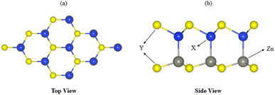 |
| | Fig. 1 Top (a) and side (b) views of ZnMN2 (M = Si, Ge and Sn and N = S, Se and Te) monolayers. | |
To investigate the dynamic stability of ZnMN2 (M = Ge, Sn, Si and N = S, Se, Te) monolayers, phonon band spectra were calculated using the phonopy code, as shown in Fig. 2. There are four atoms in each primitive unit cell, therefore, each phonon band dispersion is composed of three acoustic zero-frequency modes and 12 optical branches. It is clear from Fig. 2 that all phonon modes have positive eigenfrequencies at the Γ-point of the Brillouin zone, indicating that ZnMN2 (M = Ge, Sn, Si and N = S, Se, Te) monolayers are dynamically stable, which confirms that ZnMN2 (M = Ge, Sn, Si and N = S, Se, Te) monolayers can be experimentally synthesized in the laboratory. Furthermore, we investigated the thermal stability of these monolayers using ab initio molecular dynamics calculations. The results are presented in Fig. 3, confirm that there is no bond breaking at room temperature (300 K) to the system, hence these systems are stable at room temperature.36,39
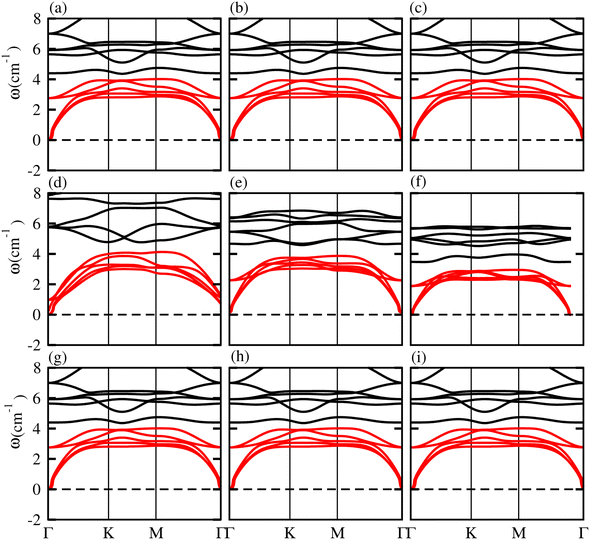 |
| | Fig. 2 Phonon band spectra of (a) ZnSiS2, (b) ZnSiSe2, (c) ZnSiTe2, (d) ZnGeS2, (e) ZnGeSe2, (f) ZnGeTe2, (g) ZnSnS2, (h) ZnSnSe2, (i) ZnSnTe2, monolayers. | |
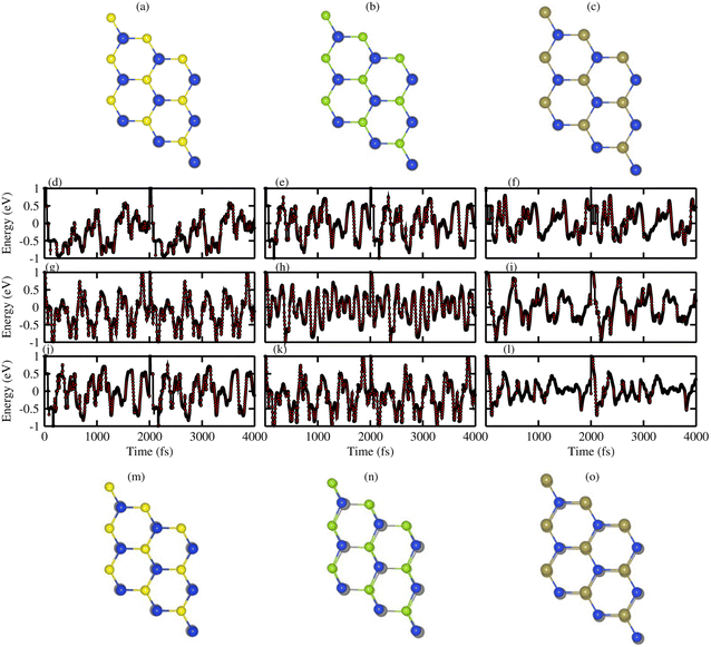 |
| | Fig. 3 AMID calculation of ZnSiN2 (N = S, Se and Te) monolayers, where (a–c) before heating; (m–o) after heating, while ((d)–(l)) is the fluctuation energy of all ZnMN2 (M = Si, Ge and Sn and N = S, Se and Te) monolayers. | |
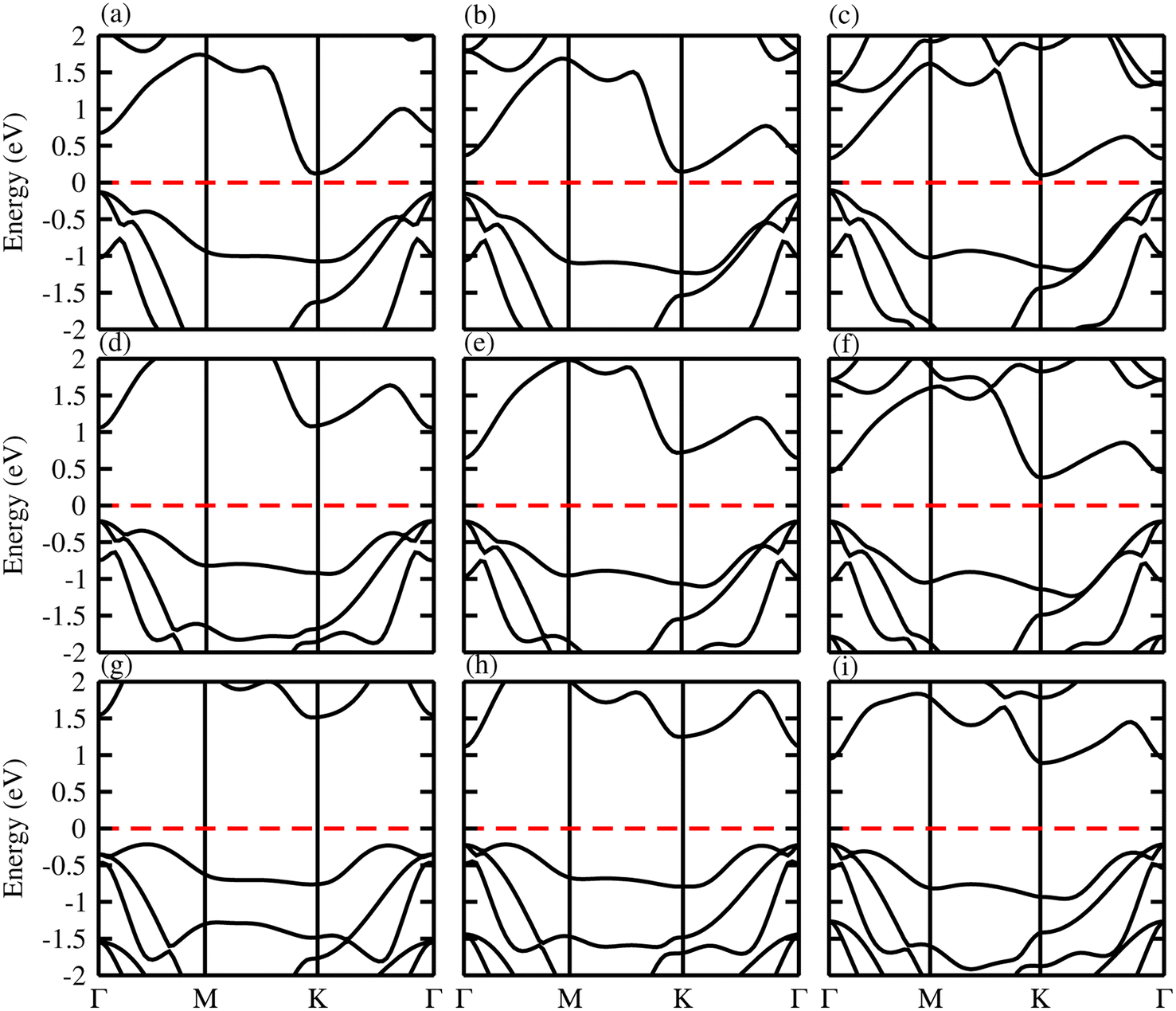
The band structure and band gap values are very sensitive to the choice of exchange correlation function, therefore, we considered both PBE and HSE06 functionals for our calculations. The calculated electronic band structures of ZnMN2 (M = Si, Ge, Sn; N = S, Se, Te) using the PBE37,38 functionals are shown in Fig. 4. One can see from the calculated electronic band structures that all the monolayers are semiconducting with a narrow band gap, and are therefore suitable for thermoelectric applications. One can also observe that ZnGeS2, ZnGeSe2 and ZnSnTe2 have a direct band gap with the CBM and VBM lying at the Γ-point, while the remaining monolayers have an indirect band gap with the VBM and CBM at the Γ- and M–Γ-points, respectively, of the first BZ. It is also observed that due to the chalcogen atom bonded to Zn and Si, the band gap values drop from S to Te. The calculated values are listed in Table 2 and are in good agreement with previous available data.19
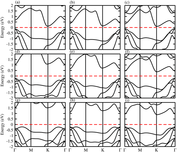 |
| | Fig. 4 Calculated band structure of (a) ZnSiS2, (b) ZnSiSe2, (c) ZnSiTe2, (d) ZnGeS2, (e) ZnGeSe2, (f) ZnGeTe2, (g) ZnSnS2, (h) ZnSnSe2 and (i) ZnSnTe2 monolayers. | |
Table 2 Calculated values of the Seebeck coefficient (S), electrical conductivity (σ) and power factor (PF) at 300 K and 800 K for the p-type doped region of ZnSiS2, ZnSiSe2, ZnSiTe2, ZnGeS2, ZnGeSe2, ZnGeTe2, ZnSnS2, ZnSnSe2 and ZnSnTe2 monolayers.
| Monolayers |
300 K |
800 K |
|
S (μV/K) |
σ (1/Ω ms) |
PF (Wm K2 s) |
S (μV/K) |
σ (1/Ω ms) |
PF (Wm K2 s) |
| ZnSiS2 |
450 |
0.89 × 10²⁰ |
0.59 × 10¹¹ |
230 |
0.8 × 10²⁰ |
1.2 × 10¹¹ |
| ZnSiSe2 |
500 |
0.95 × 10²⁰ |
0.5 × 10¹¹ |
250 |
0.9 × 10²⁰ |
1.4 × 10¹¹ |
| ZnSiTe2 |
200 |
0.9 × 10²⁰ |
0.55 × 10¹¹ |
120 |
0.86 × 10²⁰ |
1.5 × 10¹¹ |
| ZnGeS2 |
500 |
0.90 × 10²⁰ |
1.00 × 10¹¹ |
800 |
0.60 × 10²⁰ |
2.00 × 10¹¹ |
| ZnGeSe2 |
1800 |
1.00 × 10²⁰ |
0.70 × 10¹¹ |
650 |
0.70 × 10²⁰ |
2.50 × 10¹¹ |
| ZnGeTe2 |
1200 |
0.80 × 10²⁰ |
0.50 × 10¹¹ |
400 |
0.70 × 10²⁰ |
2.20 × 10¹¹ |
| ZnSnS2 |
1000 |
0.90 × 10²⁰ |
0.80 × 10¹¹ |
350 |
0.80 × 10²⁰ |
1.40 × 10¹¹ |
| ZnSnSe2 |
2000 |
0.70 × 10²⁰ |
1.30 × 10¹¹ |
800 |
0.60 × 10²⁰ |
2.00 × 10¹¹ |
| ZnSnTe2 |
1400 |
0.40 × 10²⁰ |
0.30 × 10¹¹ |
400 |
0.30 × 10²⁰ |
0.70 × 10¹¹ |
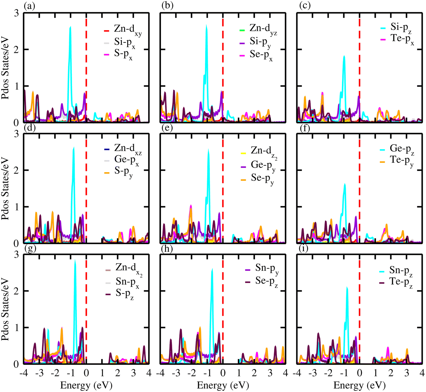
For further verification of the various atomic states of the monolayers, we computed the partial density of states (PDOS) of ZnXY2 monolayers, which are depicted in Fig. 5. The contributions of different states of the atoms are shown by different colors. From the PDOS of the ZnSiS2, ZnSiSe2 and ZnSiTe2 monolayers, it can be clearly seen that in the VBM the major contribution is due to the Te-pz atom, whereas the CBM is generated by the S, Se and Te-pz atoms. In the second row which shows results for the ZnGeS2, ZnGeSe2 and ZnGeTe2 monolayers, the VBM and CBM are due to the Ge and chalcogen pz atoms, respectively. While in the third row, which shows results for ZnSnS2, ZnSnSe2 and ZnSnTe2 monolayers, the VBM and CBM are from the Sn-pz and chalcogen pz states. In all these monolayers, some little contributions are also present due to Zn atoms. High mobility may be favored by this type of partially ionic nature with cross-gap hybridization.40
 |
| | Fig. 5 Partial density of states (PDOS) for (a) ZnSiS2, (b) ZnSiSe2, (c) ZnSiTe2, (d) ZnGeS2, (e) ZnGeSe2, (f) ZnGeTe2, (g) ZnSnS2, (h) ZnSnSe2 and (i) ZnSnTe2 monolayers in which the contributions of different atoms are labelled in the figure. | |
The absorption spectra of systems are measured to investigate the optical properties of materials. They allow the dielectric function ε2(ω)![[thin space (1/6-em)]](https://www.rsc.org/images/entities/char_2009.gif) 46 to be determined, therefore absorption spectra are a fundamental tool for understanding the interaction of electromagnetic radiation with matter. The imaginary part of the dielectric function ε2(ω) was calculated for the different monolayers and the results are shown in Fig. 6. Exciton peaks can clearly be seen for ZnSiS2 (0.96 eV), ZnSiSe2 (0.72 eV), ZnSiTe2 (0.662 eV), ZnGeS2 (0.61 eV), ZnGeSe2 (0.661 eV), ZnGeTe2 (0.64 eV), ZnSnS2 (0.52 eV), ZnSnSe2 (0.63 eV) and ZnSnTe2 (0.67 eV). These values indicate strong modifications in the positions of excitons from the S atom to the Te atom, suggesting that this is promising for controlling the exciton–phonon interactions or coupling at the nanoscale, and for applications in thermal imaging sensors in the future.47
46 to be determined, therefore absorption spectra are a fundamental tool for understanding the interaction of electromagnetic radiation with matter. The imaginary part of the dielectric function ε2(ω) was calculated for the different monolayers and the results are shown in Fig. 6. Exciton peaks can clearly be seen for ZnSiS2 (0.96 eV), ZnSiSe2 (0.72 eV), ZnSiTe2 (0.662 eV), ZnGeS2 (0.61 eV), ZnGeSe2 (0.661 eV), ZnGeTe2 (0.64 eV), ZnSnS2 (0.52 eV), ZnSnSe2 (0.63 eV) and ZnSnTe2 (0.67 eV). These values indicate strong modifications in the positions of excitons from the S atom to the Te atom, suggesting that this is promising for controlling the exciton–phonon interactions or coupling at the nanoscale, and for applications in thermal imaging sensors in the future.47
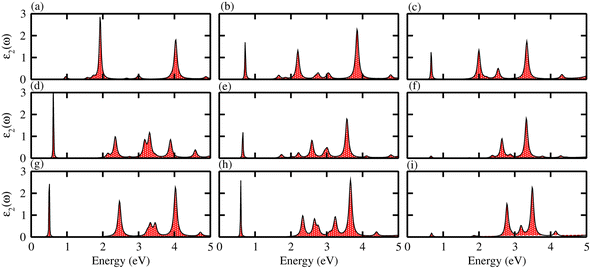 |
| | Fig. 6 Optical spectra of (a) ZnSiS2, (b) ZnSiSe2, (c) ZnSiTe2, (d) ZnGeS2, (e) ZnGeSe2, (f) ZnGeTe2, (g) ZnSnS2, (h) ZnSnSe2 and (i) ZnSnTe2 monolayers. | |
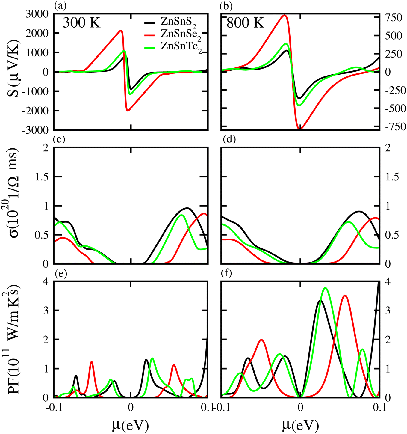
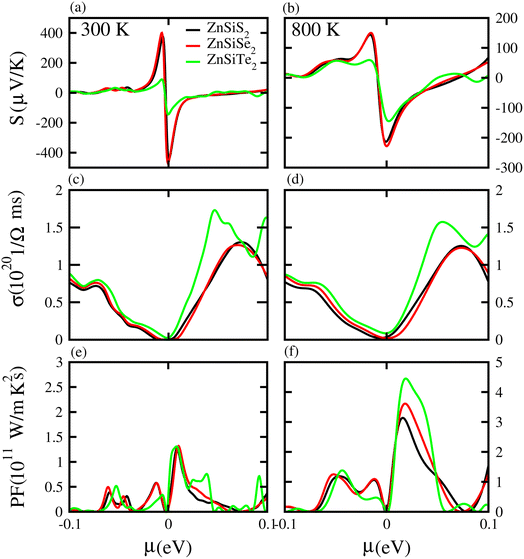
Based on the Boltzmann theory,41 we calculated transport coefficients such as the Seebeck coefficient, electrical conductivity, and power factor against chemical potential. The Seebeck coefficient is a quantified measurement of convinced voltage,42 and the Seebeck coefficient of a material represents the magnitude of the thermoelectric voltage induced by a temperature difference across the material.45 The Seebeck coefficient at (a) 300 K and (b) 800 K for ZnSiS2 (black), ZnSiSe2 (red) and ZnSiTe2 (green) is presented in Fig. 7 plotted against the chemical potential, and the Seebeck coefficient values for the n-type doped region are given in Table 2 and those for the p-type doped region are given in Table 3. The Seebeck coefficient results for ZnGeS2, ZnGeSe2 and ZnGeTe2 are shown in Fig. 8, and the values for the n-type doped region are given in Table 2 and those for the p-type doped region are given in Table 3. The Seebeck coefficient results for ZnSnS2, ZnSnSe2 and ZnSnTe2 are shown in Fig. 9, and the values for the n-type doped region are given in Table 2 and those for the p-type doped region are given in Table 3. From our calculations, it is clear that ZnSnSe2 has a greater value in both the n-type and p-type regions at 300 K and 800 K. According to the preceding discussion, ZnXY2 monolayers are p-type materials, and raising the temperature reduces the Seebeck coefficient, which makes these materials ideal for thermoelectric device applications, and similar results are also reported in ref. 43 and 44. The electrical conductivity (σ) of the materials is due to the holes and electrons in the semiconductors, and values of the electrical conductivity were calculated and plotted against μ for the ZnMN2 (M = Si, Sn and Ge and N = S, Se and Te) monolayers. For good thermoelectric materials, we need high σ values. The calculated values for σ for both n-type and p-type doped regions are given in Tables 2 and 3, respectively, for 300 K and 800 K. Our results show that ZnSiTe2 had a larger value in both the n-type and p-type regions at 300 K and 800 K. According to the preceding discussions, ZnMN2 monolayers are p-type materials, and raising the temperature reduces the Seebeck coefficient. To measure the thermoelectric power of a material, the power factor (PF) is one of the best parameters to describe the efficiency of that material with the general formula PF = σS2, where S represents the Seebeck coefficient and σ is the electrical conductivity of the material. The calculated values of the power factor at 300 K and 800 K are shown in Fig. 7 for monolayers of ZnSiS2, ZnSiSe2, and ZnSiTe2, Fig. 8 for monolayers of ZnGeS2, ZnGeSe2, and ZnGeTe2, and Fig. 9 for monolayers of ZnSnS2, ZnSnSe2 and ZnSnTe2. The values are given in Tables 2 and 3. It is obvious from Fig. 7(e, f), 8(e, f) and 9(e, f) that the peak values of the PF at both 300 K and 800 K in the p-type region are greater than in the n-type region. Furthermore, it can be seen that ZnSnS2 has a large PF at 300 K and 800 K because of its smaller Seebeck coefficient and higher electrical conductivity than ZnSiTe2, making it a promising candidate for thermoelectric applications.48
Table 3 Calculated values of the Seebeck coefficient (S), electrical conductivity (σ) and power factor (PF) at 300 K and 800 K for the n-type doped region of ZnSiS2, ZnSiSe2, ZnSiTe2, ZnGeS2, ZnGeSe2, ZnGeTe2, ZnSnS2, ZnSnSe2 and ZnSnTe2 monolayers.
| Monolayers |
300 K |
800 K |
|
S (μV/K) |
σ (1/Ω ms) |
PF (Wm K2 s) |
S (μV/K) |
σ (1/Ω ms) |
PF (Wm K2 s) |
| ZnSiS2 |
380 |
1.25 × 10²⁰ |
1.25 × 10¹¹ |
140 |
1.26 × 10²⁰ |
3.02 × 10¹¹ |
| ZnSiSe2 |
400 |
1.30 × 10²⁰ |
1.32 × 10¹¹ |
150 |
1.24 × 10²⁰ |
3.80 × 10¹¹ |
| ZnSiTe2 |
100 |
1.75 × 10²⁰ |
1.34 × 10¹¹ |
50 |
1.57 × 10²⁰ |
4.4 × 10¹¹ |
| ZnGeS2 |
500 |
0.9 × 10²⁰ |
1.50 × 10¹¹ |
700 |
1.00 × 10²⁰ |
2.2 × 10¹¹ |
| ZnGeSe2 |
1500 |
1.00 × 10²⁰ |
1.60 × 10¹¹ |
500 |
1.09 × 10²⁰ |
4.00 × 10¹¹ |
| ZnGeTe2 |
1000 |
1.10 × 10²⁰ |
1.50 × 10¹¹ |
1000 |
1.09 × 10²⁰ |
4.00 × 10¹¹ |
| ZnSnS2 |
500 |
1.00 × 10²⁰ |
1.35 × 10¹¹ |
200 |
0.90 × 10²⁰ |
2.20 × 10¹¹ |
| ZnSnSe2 |
2200 |
1.80 × 10²⁰ |
1.10 × 10¹¹ |
800 |
0.80 × 10²⁰ |
2.00 × 10¹¹ |
| ZnSnTe2 |
1000 |
0.09 × 10²⁰ |
1.45 × 10¹¹ |
350 |
0.75 × 10²⁰ |
2.50 × 10¹¹ |
 |
| | Fig. 7 Seebeck coefficient (a, b), electrical conductivity (c, d), and power factor (e, f) results for ZnSiS2, ZnSiSe2 and ZnSiTe2 monolayers at 300 K and 800 K, respectively. | |
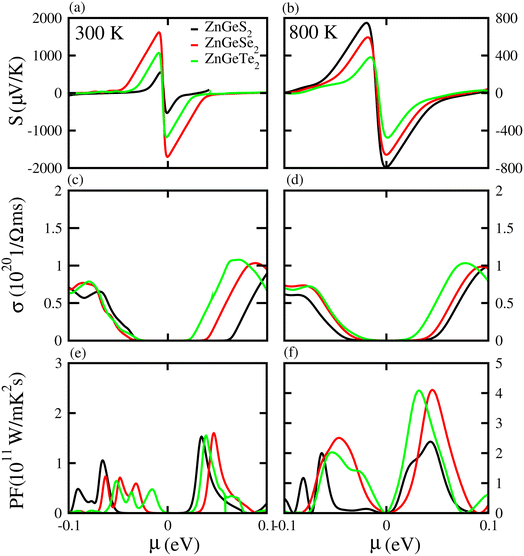 |
| | Fig. 8 Seebeck coefficient (a, b), electrical conductivity (c, d), and power factor (e, f) results for ZnGeS2, ZnGeSe2 and ZnGeTe2 monolayers at 300 K and 800 K, respectively. | |
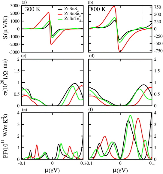 |
| | Fig. 9 Seebeck coefficient (a, b), electrical conductivity (c, d), and power factor (e, f) results for ZnSnS2, ZnSnSe2 and ZnSnTe2 monolayers at 300 K and 800 K, respectively. | |
IV. Conclusions
Using DFT, the structural, electronic, optical and thermoelectric properties of novel 2D Janus ZnMN2 (M = Si, Ge, Sn and N = S, Se, and Te) monolayers constructed according to their isoelectronic mutation have been investigated. Moreover, a direct band gap was observed in ZnSiS2, ZnSiSe2 and ZnSiTe2 monolayers, while ZnGe2, ZnGeSe2, ZnGeTe2, ZnSnS2, ZnSnSe2 and ZnSnTe2 possessed an indirect band gap. The electronic band structures revealed the semiconducting nature of the monolayers. Furthermore, values for the imaginary part of the dielectric function were calculated, which indicated strong modifications in the positions of excitons from the S atom to the Te atom, suggesting that this is promising for controlling the exciton–phonon interactions. Finally, we investigated the thermoelectric properties, including the Seebeck coefficient (S), electrical conductivity (σ), and power factor (PF), at temperatures of 300 K and 800 K, based on Boltzmann theory. The results confirmed that the peak values of the PF at 300 K and 800 K in the n-type region are greater than in the p-type region. Furthermore, it can be seen that ZnSiTe2 has a large PF at 300 K and 800 K because of its smaller Seebeck coefficient and higher electrical conductivity than ZnSnS2, making it a promising candidate for thermoelectric applications.
Conflicts of interest
There are no conflicts to declare.
Acknowledgements
The authors extend their sincere appreciation to Princess Nourah Bint Abdulrahman University Researchers Supporting Project Number (PNURSP2023R71), Princess Nourah Bint Abdulrahman University, Riyadh, Saudi Arabia.
References
- G. Zhang and Y. W. Zhang, Mech. Mater., 2015, 91, 382–398 CrossRef.
- Z. G. Chen, G. Han, L. Yang, L. Cheng and J. Zou, Prog. Nat. Sci.: Mater. Int., 2012, 22(6), 535–549 CrossRef.
- T. Zhu, Y. Liu, C. Fu, J. P. Heremans, J. G. Snyder and X. Zhao, Adv. Mater., 2017, 29(14), 1605884 CrossRef PubMed.
- G. J. Snyder and E. S. Toberer, Nat. Mater., 2008, 7(2), 105–114 CrossRef CAS PubMed.
- M. Rull-Bravo, A. Moure, J. F. Fernandez and M. Martin-Gonzalez, RSC Adv., 2015, 5(52), 41653–41667 RSC.
- P. Sundarraj, D. Maity, S. S. Roy and R. A. Taylor, RSC Adv., 2014, 4(87), 46860–46874 RSC.
- G. Tan, L.-D. Zhao and M. G. Kanatzidis, Chem. Rev., 2016, 116(19), 12123–12149 CrossRef CAS PubMed.
- C. Gayner and K. K. Kar, Prog. Mater. Sci., 2016, 83, 330–382 CrossRef CAS.
- G. Zhang and Y.-W. Zhang, J. Mater. Chem. C, 2017, 5(31), 7684–7698 RSC.
- D. Li, C. Luo, Y. Chen, D. Feng, Y. Gong, C. Pan and J. He, ACS Appl. Energy Mater., 2019, 2(4), 2427–2434 CrossRef CAS.
- Z.-H. Ge, L.-D. Zhao, D. Wu, X. Liu, B.-P. Zhang, J.-F. Li and J. He, Mater. Today, 2016, 19(4), 227–239 CrossRef CAS.
- S. Ortega, M. Ibanez, Y. Liu, Y. Zhang, M. V. Kovalenko, D. Cadavid and A. Cabot, Chem. Soc. Rev., 2017, 46(12), 3510–3528 RSC.
- R. Kroon, D. A. Mengistie, D. Kiefer, J. Hynynen, J. D. Ryan, L. Yu and C. Muller, Chem. Soc. Rev., 2016, 45(22), 6147–6164 RSC.
- A. Betal, J. Bera and S. Sahu, Comput. Mater. Sci., 2021, 186, 109977 CrossRef CAS.
- P. Mishra, D. Singh, Y. Sonvane and R. Ahuja, Sustainable Energy Fuels, 2020, 4, 2363–2369 RSC.
- K. S. Novoselov, A. K. Geim, S. V. Morozov, D. Jiang, Y. Zhang, S. V. Dubonos, I. V. Grigorieva and A. A. Firsov, Sci. Adv., 2004, 306, 666–669 CAS.
- S. Yuan, Q. Zhou and S. Li, Nano Lett., 2018, 18, 3172–3179 CrossRef CAS PubMed.
- Z. Wei, W. Zhu and F. Wang, Small Methods, 2018, 2, 1800094 CrossRef.
- T. T. Zhang, Y. Liang, H. Guo, H. Fan and X. Tian, Appl. Surf. Sci., 2022, 579, 152017 CrossRef CAS.
- S. S. Demirci, N. Avazlı, E. Durgun and S. Cahangirov, Phys. Rev. B, 2017, 95, 115409 CrossRef.
- Z. Hu, Y. Ding, X. Hu, W. Zhou, X. Yu and S. Zhang, Nanotechnology, 2019, 30, 252001 CrossRef CAS PubMed.
- M. Naguib, O. Mashtalir, M. R. Lukatskaya, B. Dyatkin, C. Zhang, V. Presser, Y. Gogotsi and M. W. Barsoum, Chem. Commun., 2014, 50, 7420–7423 RSC.
- A.-Y. Lu, H. Zhu, J. Xiao, C.-P. Chuu, Y. Han, M.-H. Chiu, C.-C. Cheng, C.-W. Yang, K.-H. Wei and Y. Yang, Nat. Nanotechnol., 2017, 12, 744 CrossRef CAS PubMed.
- T. Zhang, Y. Liang, H. Guo, H. Fan and X. Tian, Appl. Surf. Sci., 2022, 579, 152017 CrossRef CAS.
- L.-D. Zhao, S.-H. Lo, Y. Zhang, H. Sun, G. Tan, C. Uher, C. Wolverton, V. P. Dravid and M. G. Kanatzidis, Nature, 2014, 508(7496), 373–377 CrossRef CAS PubMed.
- C. Chang, M. Wu, D. He, Y. Pei and C.-F. Wu,
et al.
, Science, 2018, 360(6390), 778 CrossRef CAS PubMed.
- H. Babaei, J. M. Khodadadi and S. Sinha, Appl. Phys. Lett., 2014, 105(19), 193901 CrossRef.
- S.-D. Guo, Y.-F. Li and X.-S. Guo, Comput. Mater. Sci., 2019, 161, 16–23 CrossRef CAS.
- J. Bera, A. Betal and S. Sahu, J. Alloys Compd., 2021, 872, 159704 CrossRef CAS.
- P. Giannozzi, S. Baroni, N. Bonini, M. Calandra, R. Car, C. Cavazzoni, D. Ceresoli, G. L. Chiarotti, M. Cococcioni, I. Dabo, A. Dal Corso, S. de Gironcoli, S. Fabris, G. Fratesi, R. Gebauer, U. Gerstmann, C. Gougoussis, A. Kokalj, M. Lazzeri, L. Martin-Samos, N. Marzari, F. Mauri, R. Mazzarello, S. Paolini, A. Pasquarello, L. Paulatto, C. Sbraccia, S. Scandolo, G. Sclauzero, A. P. Seitsonen, A. Smogunov, P. Umari and R. M. Wentzcovitch, J. Phys.: Condens. Matter, 2009, 21, 395502 CrossRef PubMed.
- J. P. Perdew, K. Burke and M. Ernzerhof, Phys. Rev. Lett., 1996, 77, 3865 CrossRef CAS PubMed.
- J. P. Perdew, K. Burke and M. Ernzerhof, Phys. Rev. Lett., 1998, 80, 891 CrossRef CAS.
- S. Yousuf and D. C. Gupta, Results Phys., 2019, 12, 1382–1386 CrossRef.
- I. Ahmad, S. A. Khan, M. Idrees, M. Haneef, I. Shahid, H. U. Din, S. A. Khan and B. Amin, Phys. B, 2018, 545, 113–118 CrossRef CAS.
- B. Amin, T. P. Kaloni and U. Schwingenschlögl, RSC Adv., 2014, 4, 34561–34565 RSC.
- Q. Alam, S. Muhammad, M. Idrees, N. V. Hieu, N. T. T. Binh, C. Nguyen and B. Amin, RSC Adv., 2021, 11, 14263–14268 RSC.
- J. P. Perdew, K. Burke and M. Ernzerhof, Phys. Rev. Lett., 1996, 77, 3865 CrossRef CAS PubMed.
- J. Heyd, G. E. Scuseria and M. Ernzerhof, J. Chem. Phys., 2003, 118, 8207–8215 CrossRef CAS.
- H. U. Din, M. Idrees, Q. Alam and B. Amin, Appl. Surf. Sci., 2021, 568, 150846 CrossRef CAS.
- X. He, D. J. Singh, P. Boon-On, M.-W. Lee and L. Zhang, J. Am. Chem. Soc., 2018, 140, 18058–18065 CrossRef CAS PubMed.
- X. He and L.-S. Luo, Phys. Rev. E: Stat., Nonlinear, Soft Matter Phys., 1997, 56, 6811 CrossRef CAS.
- Q. Zhu, H. S. Kim and Z. Ren, Rev. Sci. Instrum., 2017, 88, 094902 CrossRef PubMed.
- F. Khan, H. U. Din, S. A. Khan, G. Rehman, M. Bilal, C. V. Nguyen, I. Ahmad, L.-Y. Gan and B. Amin, J. Phys. Chem. Solids, 2019, 126, 304–309 CrossRef CAS.
- K. Bashir, M. Bilal, B. Amin, Y. Chen and M. Idrees, RSC Adv., 2023, 13, 9624–9635 RSC.
- Z. Zhou and C. Uher, Rev. Sci. Instrum., 2005, 76, 023901 CrossRef.
- R. L. Olmon, B. Slovick, T. W. Johnson, D. Shelton, S.-H. Oh, G. D. Boreman and M. B. Raschke, Phys. Rev. B: Condens. Matter Mater. Phys., 2012, 86, 235147 CrossRef.
- M. Müller, W. Budde, R. Gottfried-Gottfried, A. Hübel, R. Jähne and H. Kück, Sens. Actuators, A, 1996, 54, 601–605 CrossRef.
- H. Y. Lv, W. J. Lu, D. F. Shao, H. Y. Lu and Y. P. Sun, J. Mater. Chem. C, 2016, 4, 4538–4545 RSC.
|
| This journal is © The Royal Society of Chemistry 2024 |
Click here to see how this site uses Cookies. View our privacy policy here. 
 Open Access Article
 This Open Access Article is licensed under a
  a,
Tahani A.
Alrebdi
b,
Bin
Amin
a,
Tahani A.
Alrebdi
b,
Bin
Amin