
 Open Access Article
 This Open Access Article is licensed under a Creative Commons Attribution-Non Commercial 3.0 Unported Licence
Optoelectronic synapses based on a triple cation perovskite and Al/MoO3 interface for neuromorphic information processing†
Haoliang
Sun
 ab,
Haoliang
Wang
b,
Shaohua
Dong
*a,
Shijie
Dai
b,
Xiaoguo
Li
b,
Xin
Zhang
b,
Liangliang
Deng
b,
Kai
Liu
b,
Fengcai
Liu
b,
Hua
Tan
b,
Kun
Xue
a,
Chao
Peng
ad,
Jiao
Wang
b,
Yi
Li
ac,
Anran
Yu
*b,
Hongyi
Zhu
*ac and
Yiqiang
Zhan
*b
ab,
Haoliang
Wang
b,
Shaohua
Dong
*a,
Shijie
Dai
b,
Xiaoguo
Li
b,
Xin
Zhang
b,
Liangliang
Deng
b,
Kai
Liu
b,
Fengcai
Liu
b,
Hua
Tan
b,
Kun
Xue
a,
Chao
Peng
ad,
Jiao
Wang
b,
Yi
Li
ac,
Anran
Yu
*b,
Hongyi
Zhu
*ac and
Yiqiang
Zhan
*b
aPeng Cheng Laboratory, Shenzhen 518055, China. E-mail: lightdong@yeah.net; hyzhu@bnc.org.cn
bCenter for Micro Nano Systems, School of Information Science and Technology (SIST), Fudan University, Shanghai 200433, China. E-mail: aryu@fudan.edu.cn; yqzhan@fudan.edu.cn
cShanghai Engineering Research Center for Broadband Technologies and Applications, Shanghai 200436, China
dState Key Laboratory of Advanced Optical Communication Systems and Networks, Department of Electronics and Frontiers Science Center for Nano-optoelectronics, Peking University, Beijing 100080, China
First published on 6th December 2023
Abstract
Optoelectronic synaptic transistors are attractive for applications in next-generation brain-like computation systems, especially for their visible-light operation and in-sensor computing capabilities. However, from a material perspective, it is difficult to build a device that meets expectations in terms of both its functions and power consumption, prompting the call for greater innovation in materials and device construction. In this study, we innovatively combined a novel perovskite carrier supply layer with an Al/MoO3 interface carrier regulatory layer to fabricate optoelectronic synaptic devices, namely Al/MoO3/CsFAMA/ITO transistors. The device could mimic a variety of biological synaptic functions and required ultralow-power consumption during operation with an ultrafast speed of >0.1 μs under an optical stimulus of about 3 fJ, which is equivalent to biological synapses. Moreover, Pavlovian conditioning and visual perception tasks could be implemented using the spike-number-dependent plasticity (SNDP) and spike-rate-dependent plasticity (SRDP). This study suggests that the proposed CsFAMA synapse with an Al/MoO3 interface has the potential for ultralow-power neuromorphic information processing.
1. Introduction
As a simulation of the real human brain neural networks, artificial neural networks (ANNs) have been widely used in various fields and have become the most mainstream artificial intelligence models, which are usually implemented in the form of software algorithms on electronic computers.1–3 Traditional electronic computers, which are based on von Neumann architecture, significantly outperform human beings in terms of logical computing tasks. However, in the field of artificial vision, such as pattern recognition and target detection, traditional computers, which are rooted in the compute-storage separation architecture, are not only significantly incompetent but also energy-wasteful compared with human beings.4,5 Owing to the progress in bionics and micro/nano electronics, memristor-type electronic devices have now been developed for simultaneously storing and processing data.6–9 Memristor-type devices, called artificial synaptic devices, have been widely studied because they can effectively simulate the working mechanism of human neurons and synapses.10–12 This is usually considered as the underlying device for implementing brain-like sensing and computing.13–15 Unlike pure electronic synaptic devices, which are limited by the transmission bandwidth and energy consumption, optoelectronic synaptic devices have the advantages of both photics and electrics, such as the reception and transmission of photics and the storage and processing of electrics.16–19Therefore, significant efforts have been made to simulate synaptic plasticity using micro/nano-optoelectronic synaptic devices. Zhou's team developed an optoelectronic resistive random-access memory (ORRAM) for 365 nm light based on Pd/MoOx/ITO.20 Hu's research team fabricated a photoelectric memristive synapse based on an ITO/ZnO1−x/AlOy/Al device structure that could work under UV-light illumination.21 However, in these previous studies, most photosensitive phase transitions occurred in the high-energy region of the spectrum (such as ultraviolet or above), which means that they could not effectively respond in the visible-light range. Thus, an artificial vision response mechanism cannot be constructed in the visible-light range. The inability to operate in the visible-light range fundamentally restricts the development of optoelectronic synaptic devices for matching human vision. Recently, Cheng's team reported a novel neuromorphic–photoelectric device of vertical van der Waals heterojunction phototransistors based on a colloidal 0D-CsPbBr3-quantum-dot/2D-MoS2 heterojunction channel, which displayed photoelectric plasticity and synaptic functions.22 Reservoir computing (RC) is a simple and efficient brain-like algorithm for processing temporal signals. In RC systems, a dynamic “reservoir” of synapses with short-range plasticity are used to map complex temporal signals to a new space, represented by the states of the nodes in the reservoir. More recently, studies have shown that devices based on optoelectronic synapses can support RC and consequently, have been successful used in the field of artificial vision.23–27 These studies are noteworthy. However, compared with the functional layer materials and device structures used in traditional perovskite batteries, some materials and device structures that are not commonly in perovskite batteries suffer from material mismatch, perovskite toxicity, and a difficulty of preparation.28 Therefore, on the premise of meeting the requirements of visible-light work, a more universal device structure paradigm is also needed to provide fabrication guidance and simplify the difficulty of device fabrication.
In this work, we incorporated perovskite as a photosensitive material and combined it with an Al/MoO3 heterojunction into an optoelectronic synaptic device that could operate in the visible-light range and effectively simulate a variety of synaptic functions at an ultralow energy consumption, such as excitatory postsynaptic current (EPSC), paired-pulse facilitation (PPF), short-term plasticity (STP), long-term plasticity (LTP), and forgetting behavior. Notably, the material and structural composition of this synaptic device were based on materials and structures common to perovskite solar cell devices. Furthermore, we demonstrated both the applications of classical Pavlovian conditioning and image signal encoding processing, where the former showed the value of the device in associative learning and the latter could support the use of in-sensor RC in visual perception.
2. Results and discussion
Organic–inorganic halide perovskites (OIHPs) are widely used in optoelectronic devices because of their excellent photoelectric conversion efficiency, high stability, and controllable bandgap compared with non-hybrid perovskites.29 Among them, triple cation perovskites with excellent thermal and structural stability, especially CsFAMA, can be prepared by optimizing the ratio of the cationic and halogen ion elements in perovskite.30 Based on this, we explored and optimized the preparation protocol for CsFAMA perovskite and introduced it as a photonic electron supply layer in our optoelectronic synapse. In addition, molybdenum oxide, a metal oxide material commonly used in optoelectronic devices, has been applied to optoelectronic synaptic devices because of its oxygen defect characteristics.20 Inspired by this, we attempted to simulate the synaptic function in synaptic devices by introducing an Al/MoO3 layer to obtain sufficient oxygen defects in the optoelectronic devices to control the dynamic behavior of carriers.2.1. Device structure, photoresponse, and energy consumption
The human visual system can directly receive and send rudimentarily processed optical signals into the brain. Synapses between the eyes and brain act as important links that take charge of information reception, simple processing, and transmission (Fig. 1a). To simulate and integrate the functions of synapses in the human visual system, we remodeled the photoreceptors based on two-terminal CsFAMA perovskite transistors with an oxygen-defect-abundant layer, making the device both capable of responding and processing optical signals into a couplable EPSC. As illustrated in Fig. 1a, our designed two-terminal optoelectronic synaptic device demonstrated a stacking structure, with Al on the top, MoO3 and CsFAMA perovskite successively in the middle, and ITO at the bottom. Fig. 1b shows a cross-section scanning electron microscopy (SEM) image and illustrates the order and thickness of the individual layers, with CsFAMA 500 nm thick, MoO3 40 nm, and Al 80 nm. From the SEM image, it can be seen that each layer was well prepared, and the perovskite layer showed the characteristics of compactness and uniformity. To explore the resistive switching and photoresponse character of this device, typical current–voltage (I–V) curves of the Al/MoO3/CsFAMA/ITO device were measured in the darkness and under visible-light illumination, as shown in Fig. S1 in the ESI.† In the high-resistance state (HRS), it was clear that different resistive switching behaviors existed between the darkness (Fig. 1c black) and under illumination (Fig. 1c red) conditions. This measurement shows that the conductivity of the device was raised by several times in the HRS part, indicating the device was affected by light stimulation and could respond to light signals.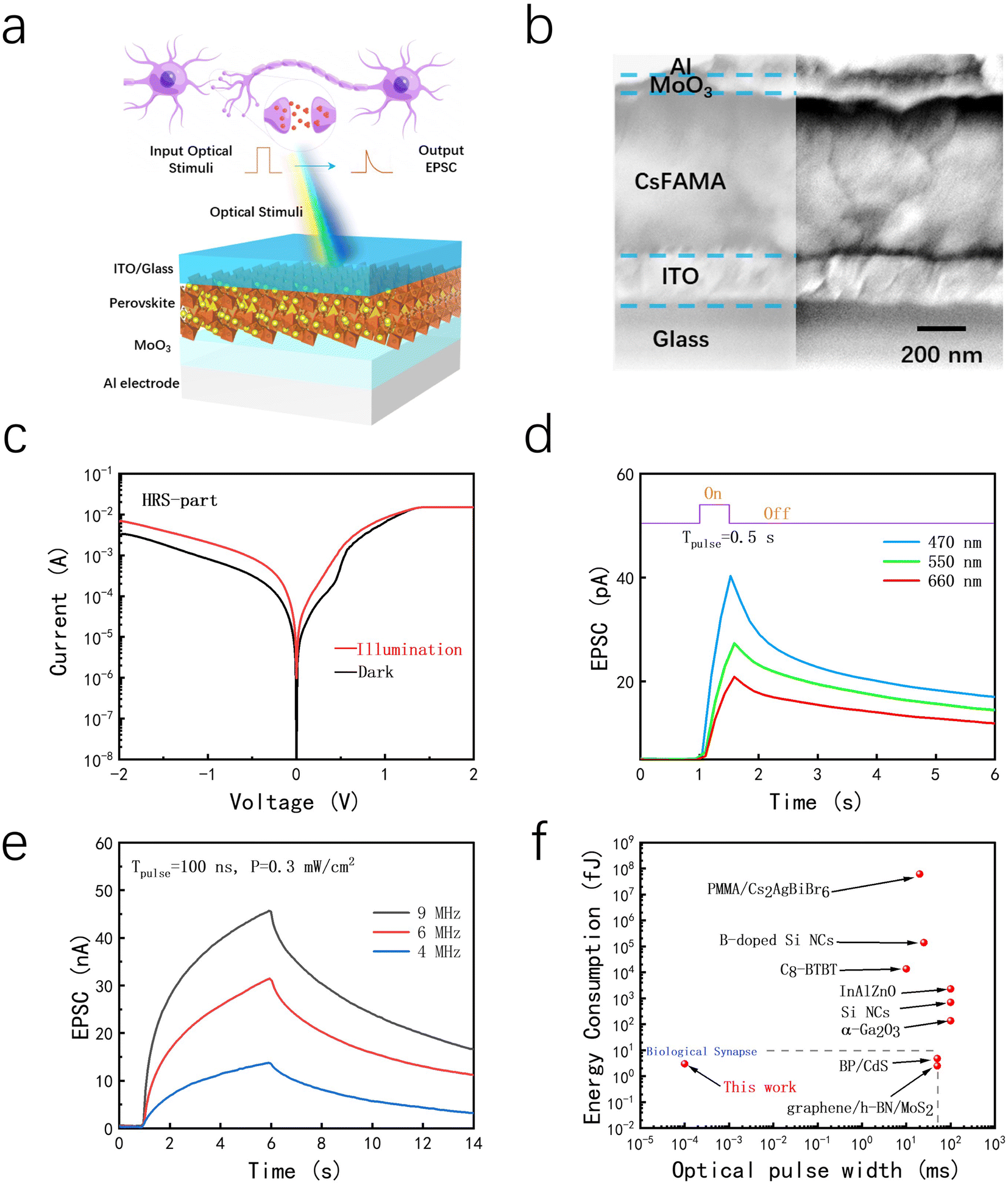 | ||
| Fig. 1 Device structure, photoresponse, and energy consumption of the CsFAMA optoelectronic synaptic transistor. (a) Schematic of biological synapses and the corresponding synaptic transistors. (b) Cross-sectional scanning electron microscopy (SEM) image of the device. (c) I–V curves (HRS part) of the synaptic transistor in the dark (black line) and under light illumination (red line). (d) Photoresponse with different wavelengths. (e) Minimum pulse widths (Tpulse = 100 ns, P = 0.3 mW cm−2) of the light response at different frequencies. (f) Comparison of the single optical pulse width and power consumption among some optoelectronic synaptic devices. Measurements of (d) and (e) were performed at 0 V bias. | ||
In order to further explore how the device responds to optical signals and take full advantage of the wide spectral characteristics of perovskite in the visible range (Fig. S2, ESI†),31 light with the same power and width, but different wavelengths (470, 550, and 660 nm) was used to stimulate the device (Fig. 1b). The bias voltage (V) of 0 V was applied for all the following measurements. According to Fig. 1b, the CsFAMA synapse showed a typical synaptic property; that is, the effects after the stimulation (EPSC) did not disappear immediately with the disappearance of the stimulus. Moreover, the strength of the effects (i.e., the intensity and duration of EPSC) was correlated with the wavelength, and this phenomenon may be the reason for the linearly decreasing absorptive capacity of CsFAMA perovskite.
In our CsFAMA optoelectronic synapses, an extreme response time was demonstrated by light stimulation at different frequencies (4, 6, and 9 MHz, λ = 470 nm, P = 0.3 mW cm−2), as shown in Fig. 1e. As is well known, the most essential feature of a synapse is the PPF effect, whereby continuous stimulation leads to a continuous increase in synaptic weight. In Fig. 1e, it could be obviously found that the strength of the EPSC was affected by all three different frequencies of light, meaning that a light pulse with a fix width of 0.1 μs would be enough to trigger the plasticity of the device. The time of 0.1 μs was ultrafast compared to even the instantaneous information transmission in biological synapses, which is typically considered to be 50 ms and relies on neurotransmitters to transmit information.32 The ultrafast transmission speed of our synaptic transistors was due to the ultrafast photoelectron conversion speed of the perovskite and the relatively short relaxation time of the charge carriers. In general, the energy consumption of one synaptic event can be estimated by the following equation:14,33,34
| E = Ipeak × Vread × t, | (1) |
2.2. Tunable EPSC and the working mechanism of the CsFAMA optoelectronic synapses
As shown in Fig. 1, the Al/MoO3/CsFAMA/ITO device exhibited typical synaptic properties, and the amplitude of the EPSC continually increased with the frequency of light pulses. In contrast, without the MoO3 layer, the Al/CsFAMA/ITO device exhibited a transient photocurrent following the light pulses, and the amplitude was not enhanced with an increase in the pulse number (Fig. S3, ESI†). From this comparative test, we can see that the MoO3 layer plays a crucial role in the Al/MoO3/CsFAMA/ITO synaptic transistor.To discover the working mechanism of our optoelectronic synapses, XPS was performed to confirm the stoichiometry variation of the Al/MoO3 interface. Fig. 2a and b shows the core-level scan XPS data for Al 2p and Mo 3d, respectively. It can be fairly recognizable from the Al 2p spectrum that there were mainly two types of element peaks (Fig. 1c), with one peak at 73.0 eV representing metallic Al, and another peak with a higher band energy (around 75.0 eV) originating from the oxidation state of Al.46 In addition, the 75.0 eV peak showed a characteristic of being wide and short (crossing from 72.0 eV to 78.0 eV), indicating that the oxidized Al was not concentrated in a fixed valence state (such as Al2O3), but was non-stoichiometric AlOy.21 In Fig. 1d, the Mo 3d region displayed two pairs of peaks (blue and orange), representing the typical spin–orbit splitting states of 3d5/2 and 3d3/2 in Mo 3d. The blue pair of peaks for Mo 3d3/2 (236.0 eV) and Mo 3d5/2 (233.0 eV) fitted the Mo6+ states well, which originated from the MoO3 layer.47 There also existed another much stronger pair of orange peaks for Mo 3d3/2 (233.0 eV) and Mo 3d5/2 (230.0 eV), which suggested the formation of large Mo4+ ions induced by a reduction reaction. Overall, the Al 2p and Mo 3d XPS data clearly indicated that redox reactions occurred at the Al/MoO3 interface, resulting in the presence of non-stoichiometric AlOy and MoOx. Combining this knowledge with the band energies of Al, MoO3, CsFAMA, and ITO materials obtained from the literature,48,49 we were able to draw the energy band diagram for the Al/MoO3/CsFAMA/ITO device under optical stimulus (Fig. 2c). According to the literature, the work function of Al is 4.3 eV, but due to the action of MoO3, Al and MoO3 will form a mixture alloy at the interface, and the mixture AlOy/MoOx has been shown to have a work function of 5.3 eV. This alloy (5.3 eV) electrode and ITO electrode (4.7 eV) constitute an internal electric field pointing out from ITO to Al. With the assistance of the internal electric field, the photogenerated holes in the perovskite will move toward the Al electrode.50 As shown in Fig. 2d, due to the existence of a large number of oxygen vacancies at the Al/MoO3 interface, an energy potential well will be provided for the hole carriers. These hole carriers will be bound by the potential well and cannot quickly move to the metal Al interface to compound with electrons. When the light source disappears, the holes bound by the defects will continue to move to the Al electrode under the action of the internal electric field until all the bound hole carriers are released.37,51 This process greatly prolongs the relaxation time of the photocurrent and makes the device have short/long-range optical pulse plasticity. It is worth mentioning that in the research into perovskite solar cells, the molybdenum oxide layer is often used as a hole-extracting layer/electron-reflecting layer, which has very good carrier selectivity at the interface with perovskite. Therefore, the MoO3 layer here can also block electrons and regulate the direction of electron motion.
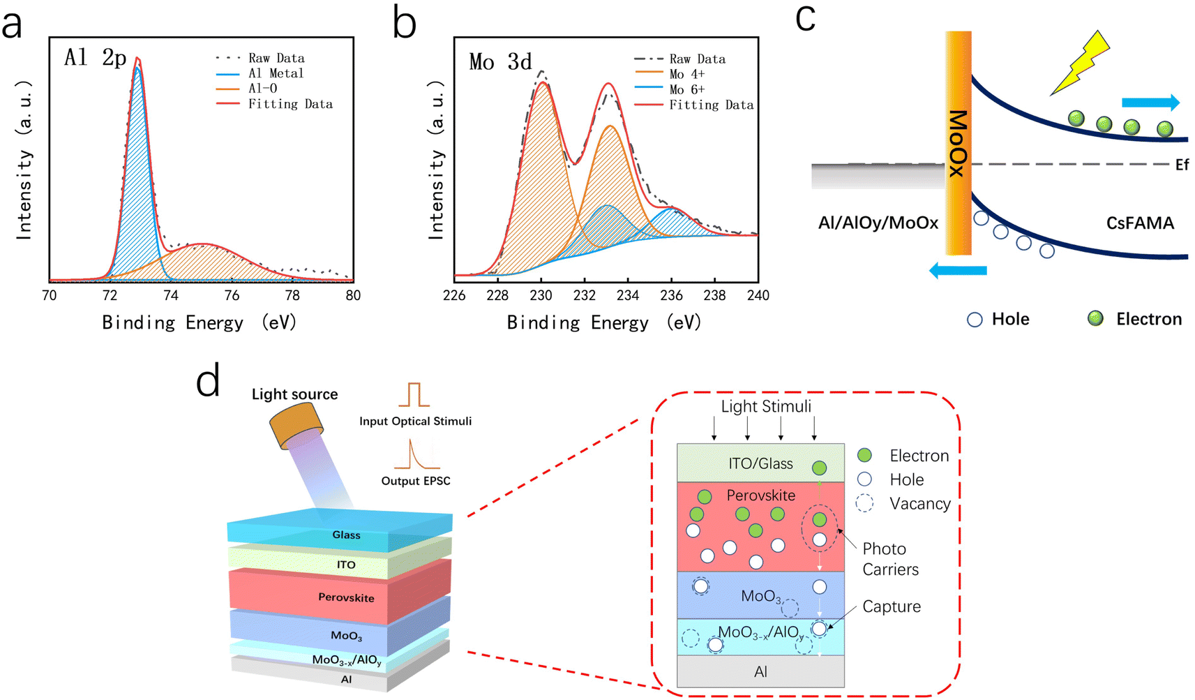 | ||
| Fig. 2 XPS studies and mechanisms of CsFAMA optoelectronic synapses. XPS spectra of (a) Al 2p and (b) Mo 3d. (c) Energy band diagram of the Al/MoO3/CsFAMA/ITO device under an optical stimulus. (d) Schematic of the device and the microscopic operation mechanism. | ||
If the captured carriers in the defects are not completely released, and another excitation light is applied to the device again, the defects will repeat the previous process on the basis of the existing captured carriers, and the device will thus exhibit an increase in photocurrent intensity and a longer release time after light removal. Here, the superposition of the previous behavior indicates that the photocurrent can be coupled; that is, the coupling of the input optical signal. This tunable EPSC behavior of the device is very similar to the behavior of biological synapses; therefore, devices based on Al/MoO3/CsFAMA/ITO can fully complete the simulation of biological synaptic behavior.
2.3. Optoelectronic synaptic functions in CsFAMA synapses
The basic neuromorphic functions in biological synapses for learning and memory are based on synaptic plasticity, which can be modulated by the number, frequency, and duration of the input signal. Neurobiologically, synaptic plasticity is divided into STP and LTP, in which the former is closely related to neuronal coding and signaling, while the latter is the basis of learning and memory.22 PPF is one of the most characteristic manifestations of STP and is often used as the basic condition to verify whether as-prepared transistors have synaptic functions. As shown in Fig. 3a, PPF could be stimulated by two successive optical pulses (P = 184 μW cm−2, width = 50 ms, Δt = 50 ms, λ = 470 nm), and the later EPSC (A2) is always higher than the former one (A1) for the EPSC coupling. The PPF ratio was calculated by the formula A2/A1 × 100%, and the magnitude of the ratio is directly affected by the interval time (Δt) between the pair of optical pulses.52Fig. 3b shows that the PPF ratio decreased from 170% to 105% as Δt increases from 16 ms to 9.9 s. The inverse relation between the PPF ratio and Δt is basically similar to what happens in biological synapses, where the weight between the anterior and posterior synapses is related to the rate of learning. The decay of the PPF index (blue dots) depending on Δt could be well fitted by the following double-exponential equation:52,53PPF = c1![[thin space (1/6-em)]](https://www.rsc.org/images/entities/char_2009.gif) exp(–Δt/τ1) + c2exp(–Δt/τ2) + 1, exp(–Δt/τ1) + c2exp(–Δt/τ2) + 1, | (2) |
We then investigated the synaptic plastic response to the pulse number and frequency; in which all the applied read voltages were 0 V. Fig. 3c shows the EPSC stimulated by the same optical pulse with different numbers of pulses of 2, 5, 8, 12, and 16, respectively. As the number of pulses increased, the EPSC showed a nonlinear growth trend from 150 pA to 250 pA. Fig. 3d meticulously shows the EPSC curves following strict coupling with the number of pulses and the capability of our optoelectronic synapse with spike-number-dependent plasticity (SNDP).54Fig. 3e shows the EPSC stimulated by different frequencies (0.5, 1, 2, 10 Hz) and the higher spike-rate stimulated the larger EPSC. Similar to spike-number stimulation, all the curves showed a trend of nonlinear growth and decay; this behavior is also referred to as spike-rate-dependent plasticity (SRDP).55 In order to find the attenuation law of the EPSC, we applied pulses of different frequencies (2, 5, 10 Hz) for a period of 1 s to the device (Fig. 3f). The decay curves of the EPSC could be extracted in Fig. 3g and well fitted by using the well-known Kohlrausch function:56
| I = I0 + A × exp[−(x/τ)β], | (3) |
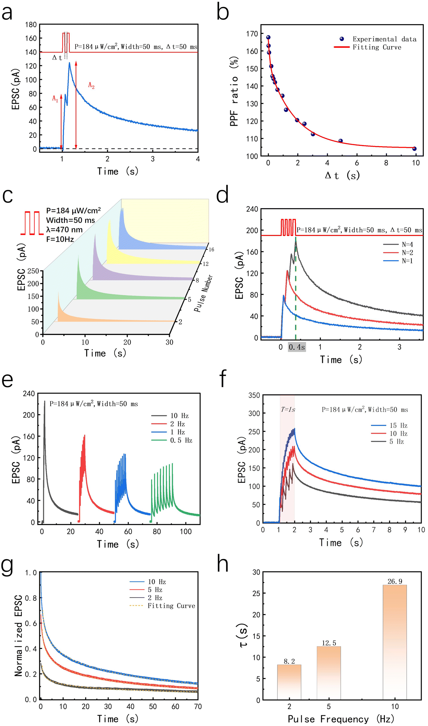 | ||
| Fig. 3 Optoelectronic synaptic functions in Al/MoO3/CsFAMA/ITO synapses. (a) Photonic PPF stimulated by a pair of optical pulses (P = 184 μW cm−2, width = 50 ms, Δt = 50 ms, λ = 470 nm). (b) PPF index (defined as A2/A1) depending on a series of time intervals (Δt). The EPSC stimulated by different (c) optical spikes, (d) numbers, (e) frequencies (10 spikes), and (f) a fixed time of T = 1 s. (g) and (h) Decay curves and time (τ) depending on different frequencies in (f). All the read voltages applied above were 0 V. | ||
2.4. Associative learning and visual perception
Associative learning in animal behavior is any learning process in which a new response is associated with a particular stimulus. In the broadest sense, the term has been used to describe virtually all learning, except for simple habituation. In a more restricted sense, it has been limited to the learning that occurs through classical and instrumental conditioning. Pavlovian conditioning is considered a signature feature of associative learning, which can be verified by the famous Pavlov's dog experiment. As shown in Fig. 4a, dogs are naturally interested in meat and salivation is induced in response to an unconditioned stimulus. When the meat changes into a bell, the dog will not salivate, as the bell is an ineffective stimulus relative to the dog's natural ability. To establish a connection between the meat and the bell, the meat and bell signals should be matched together. After training in associative learning, the dog's nervous system forms the dog's conditioned response to the bell; whereby salivation can be caused by both meat and the bell. In Fig. 4b, different rates of light pulses were applied to work as the stimulate signals. With the same light intensity and duration (1 s), 5 Hz light pulse represents the meat signal, meanwhile the 2 Hz light pulse represents the bell signal. In addition, the 100 pA EPSC was stipulated as the threshold for the dog's excitement. That is, if the value of EPSC exceeds 100 pA, stimulated by light signals, the dog (the CsFAMA synaptic transistor) responds to the signal; otherwise, the signal is ineffective. Without training, combined with the previous results (Fig. 3f), the EPSC by a 5 Hz light pulse signal could easily exceed the excitability threshold, but could not be achieved by a 2 Hz signal. In Fig. 4c, the combined 5 Hz and 2 Hz spikes were applied as training signals, and the resulting EPSC was obviously higher than the original values. Owing to the character of coupling, a higher EPSC indicates a higher overall value of the decay curve. Then, after a duration of 80 s, if the 2 Hz light pulses are applied to the transistor with different retardation times, the EPSC will show different values. Which means that after training 80 s, the bell signal could be applied as an effective stimulus (EPSC > 100 pA); after 140 s, the stimulus became weaker but was still effective (EPSC ≈ 100 pA); then after 200 s, the stimulus lost its efficacy (EPSC < 100 pA). The smaller the interval between training and stimulation, the higher decay curve it is based on, thus the first two EPSC values exceeded the threshold (100 pA), indicating that the bell became a conditioned stimulus. A conditioned response was thus successfully established between the dog and bell. However, remarkably, due to the continuous decay of the overall value in the training decay curve, the third input signal did not trigger an excitatory response in the device. This quite appropriately showed that conditioning was based on continuous training; once too long, conditioning will continue to weaken until it disappears, or it can be called forgetting. Furthermore, the pulse number effect on the Pavlovian associative learning could also be examined using the values N = 1, 4, and 5, and a rate of 10 Hz, as shown in Fig. 4d. This series of experiments revealed that Pavlovian associative learning behaviors could be successfully mimicked by the CsFAMA synaptic transistors.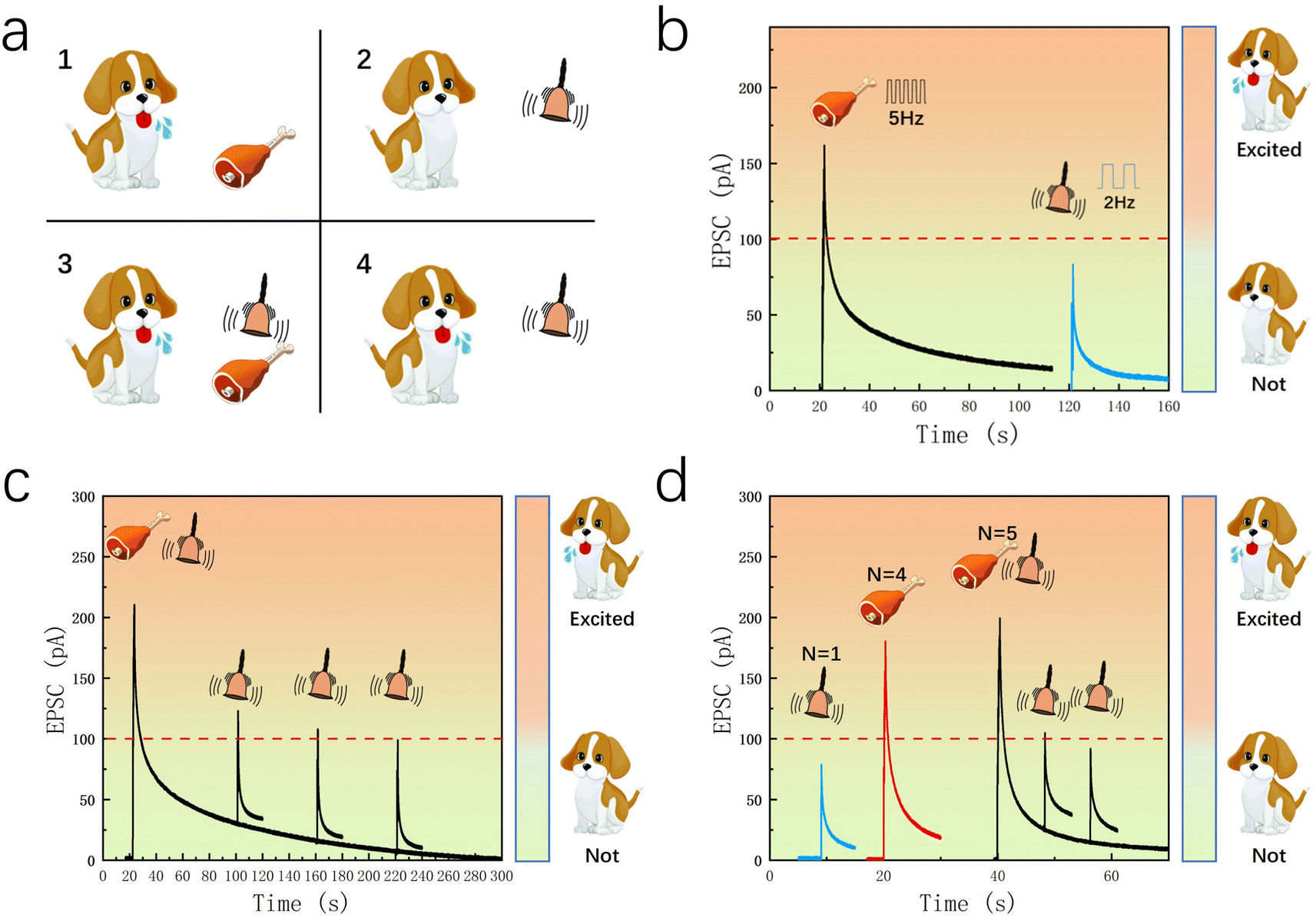 | ||
| Fig. 4 Associative learning was verified by Pavlov's dog experiment in the CsFAMA synaptic transistor. (a) Schematic illustration of Pavlov's dog experiment. (b) In the rate-based experiment, light pulses with frequencies of 5 and 2 Hz represent the stimulations of the meat and bell, respectively. (c) Training and verification of the rate-based experiment, “bell signals” applied after training for 80 s, 140 s, and 200 s. (d) Pulse number-based Pavlov's dog experiment, in which the number pulses (N = 1, 4, and 5; rate = 10 Hz) represents the bell, meat, and training. | ||
RC, also known as the echo state network, is considered a brain-like algorithm of the neural network. As shown in Fig. 5a, an RC system consists of three parts: the input, middle, and output layers.58 In the middle layer (reservoir), there is a dynamic spiking neural network that preprocesses the image pattern that comes from the input layer. The preprocessed new pattern is then sent to the output layer. Finally, the output layer uses existing machine-learning methods to learn this new pattern and obtain pattern recognition or classification. The reservoir part of RC has two requirements: it must be made up of individual nonlinear units and must be able to store information, which maps the inputs into a higher-dimensional computing space and then conducts pattern analysis in a readout section.59 Thus, the key step to implement the RC is how to build a dynamic “reservoir,” which can map complex timing signals into a new space, and reduce the difficulty of subsequent calculations. Recent studies have shown that the combination of optical synaptic devices can realize RC image-processing systems, streamline network structures, and reduce energy consumption.27,60 In the process of human eye recognition (Fig. 5a), the human eye is equivalent to the input and reservoir layers in RC, first perceiving and pretreating image information; then, the information of interest (pretreated) is transmitted to the brain to analyze or store it.
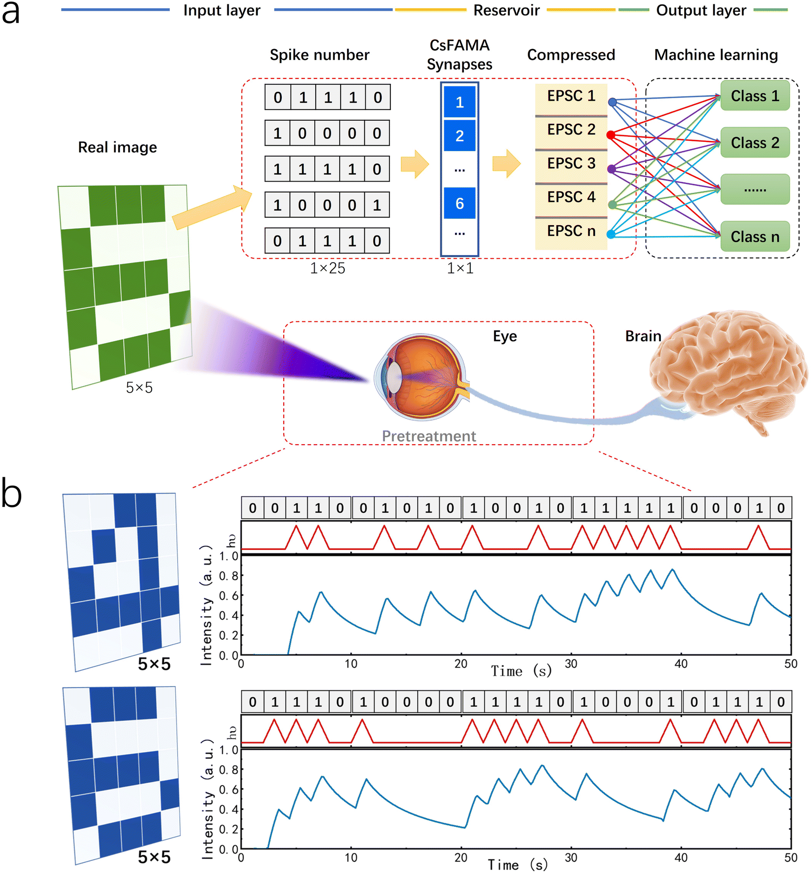 | ||
| Fig. 5 Visual perception process and reservoir computing system based on CsMAFA synapses. (a) Schematic of the neuromorphic image-processing system, including input, reservoir, and output layers. (b) Nonlinear EPSC coupling evolutions of binary digital pictures of “4” and “6”. In the binary digital picture, there is no pulse if there is no pixel, otherwise there is a pulse of 1 Hz (width = 0.5 s, Δt = 0.5 s). The pictures of “4” and “6” are represented by a series of pulses (hν) and corresponding photoexcitation current (EPSC). All the read voltage applied above were 0 V. | ||
To demonstrate the application in the built RC system, corresponding to the functions of the input layer and reservoir layer in RC, a neuromorphic image-processing system was conceptually built, based on the SNDP characteristics of the CsMAFA synaptic devices (Fig. 5b). In this neuromorphic image-processing system, the digital images of 4 and 6 were a 5 × 5 pixels image, and the gray level of 4 and 6 was transformed into “0” and “1.” For example, all the pixels of image 4 could be transformed into “0011 … 0010”, in which “1” means the optical pulse worked and “0” means that it did not. In this study, an optical pulse of 1 Hz (width = 0.5 s, Δt = 0.5 s) was chosen as the signal source because its decay intensity and time were sufficient for the experiment. Under this rule, the information of “0011 … 0010” could be represented by a series of optical pulses, as shown by the red curves in Fig. 5b. Then, the CsMAFA synapse was stimulated by the series of optical pulses and generated a coupled EPSC 1, which handled the 25 pixels information (1 × 25) into an EPSC value (1 × 1), represented by the blue curves in Fig. 5b. Referring to the above process, the image of 6 for 25 pixels (5 × 5) could also be compressed to another one for EPSC values (1 × 1). Due to the excellent nonlinear coupling ability of this synaptic device to EPSC, each EPSC value contained spatiotemporally linked characteristics. That is, the information in the image was perceptually compressed, thus reducing the dimension of the image. Subsequently, the compressed “image” was used as a new input to the following machine-learning network for the classification task. This nonlinear coupling processing is an efficient method for improving the machine-learning efficiency and reducing the computing energy consumption. During the entire process of image processing, the CsMAFA synapse array successfully imitated the role of human eyes in preprocessing (see red box in Fig. 5) and the functions of the input layer and reservoir layer in RC; therefore, the CsMAFA synapse array can be used in the application of visual perception.
3. Conclusion
In this work, we innovatively designed and constructed an optoelectronic synapse device based on an Al/MoO3/CsFAMA/ITO structure that can directly respond to visible-light signals. Owing to the excellent photoelectric conversion ability of CsMAFA perovskite and carrier regulation ability of the Al/MoO3 interface layer, the device showed a good ability of synaptic plasticity, such as EPSC, PPF, STP/LTP, and forgetting behavior. This study demonstrated a universal device structure paradigm to fabricate optoelectronic synaptic transistors that may be suitable for many photosensitive materials with little optimization cost. Meanwhile, our optoelectronic synapses can work in an ultralow-power condition due to their photovoltaic character that needs no bias voltage. Under visible-light stimulation, we demonstrated SNDP and SRDP synaptic plasticity in our devices. Also, based on the two synaptic plasticities, Pavlov's dog experiment was carried out, showing the device could be applied in associative learning. Overall, the CsMAFA synapse device exhibited great potential in a neuromorphic image-processing system by pretreating images and reducing energy consumption.4. Experimental section
4.1. Materials
DMSO (99.8%), N,N-dimethylformamide (DMF, 99.8%), chlorobenzene (CB anhydrous, 99.8%), and cesium iodide (CsI) were purchased from Sigma-Aldrich. Methylamine hydrobromide (MABr), formamidinium iodide (FAI), lead iodide (PbI2), and lead bromide (PbBr2) were purchased from Alfa Aesar. Al (99.999%) and MoO3 (99.99%) were purchased from ZhongNuo Advanced Material (Beijing) Technology Co. Ltd, China. All materials were used as received without further modifications.4.2. Film formation and device fabrication
ITO substrates were consecutively cleaned in detergent, acetone, isopropyl alcohol, and deionized water with ultrasonication for 30 min. Then, the substrates were blown dry by N2 flux and then treated with UV-ozone for 15 min just before the perovskite layer deposition. The perovskite precursor solution (I) was prepared by mixing 171.97 mg FAI, 22.79 mg MABr, 87.74 mg PbBr2, and 507.11 mg PbI2 with 800 μL DMF and 200 μL DMSO. The perovskite precursor solution (II) was prepared by mixing 194.86 mg CsI with 500 μL DMSO. Then, 45 μL precursor solution (II) was added into precursor solution (I) with continuous dissolving and heating for 5 h. After cooling down to room temperature, the perovskite precursor solution was filtered by a 0.22 μm membrane filter. The perovskite layer was fabricated by spin-coating 50 μL perovskite precursor solution on top of the ITO substrate at a speed of 5000 rpm for 30 s, inside a N2-filled glove box. At the time of 7 s to the end, 250 μL CB was quickly dropped as an antisolvent and applied to passivate the perovskite. Then the as spin-coated film was annealed at 100 °C for 1 h. After cooling down to room temperature, MoO3 (40 nm, 0.5 nm s−1) and Al (80 nm, 0.5 nm s−1) were deposited on top of the perovskite by thermal evaporation (Kurt).4.3. Material characterization
X-Ray photoelectron spectroscopy (XPS) was carried out in the laboratory using monochromatic Al Kα radiation (hν = 1486.6 eV), and the photoelectrons were collected at normal emission with a Specs electron analyzer (Phoibos 100). The photon energy was calibrated against the Au 4f7/2 core level and the metal's Fermi level, respectively. SEM images were obtained using field-emission SEM (ZEISS Sigma HD) with an accelerated electron beam at 8 kV. The absorption spectra were obtained between 300 and 1100 nm wavelength range using an F20-UV thin-film analyzer (FILMETRICS).4.4. Device characterization
The optoelectronic current responses of the device were recorded under illumination of 470 nm light (THORLABS-M470L3). The light sources with different kinds of wavelength were purchased from THORLABS. The light pulses were modulated by using an arbitrary function generator (Tektronix-AFG2021). The photoelectric measurements of the device were performed in air using a semiconductor characterization system (B1500A, Keysight Technologies) at room temperature.Conflicts of interest
The authors declare no conflicts of interest.Acknowledgements
This work was supported by the National Key R&D Program of China (No. 2020YFB1806405), Shanghai Science and Technology Innovation Action Plan (No. 23QB1400100), National Natural Science Foundation of China (No. 12004258) and the Major Key Project of PCL (No. PCL2023A04, PCL2021A17). The author thanks Dr Zhang Huan from Instrumentation and Service Center for Physical Sciences at Westlake University for the assistance supporting in XPS measurements and data interpretation.References
- S. Hochreiter and J. Schmidhuber, Long short-term memory, Neural Computation, 1997, 9(8), 1735–1780 CrossRef CAS PubMed.
- Y. Lecun, Y. Bengio and G. Hinton, Deep learning, Nature, 2015, 521(7553), 436–444 CrossRef CAS PubMed.
- J. Schmidhuber, Deep learning in neural networks: an overview, Neural Networks, 2015, 61, 85–117 CrossRef PubMed.
- P. A. Merolla, J. V. Arthur and R. Alvarez-Icaza, et al., A million spiking-neuron integrated circuit with a scalable communication network and interface, Science, 2014, 345(6197), 668–673 CrossRef CAS PubMed.
- K. Roy, A. Jaiswal and P. Panda, Towards spike-based machine intelligence with neuromorphic computing, Nature, 2019, 575(7784), 607–617 CrossRef CAS PubMed.
- D. B. Strukov, G. S. Snider and D. R. Stewart, et al., The missing memristor found, Nature, 2008, 453(7191), 80–83 CrossRef CAS PubMed.
- J. J. S. Yang, D. B. Strukov and D. R. Stewart, Memristive devices for computing, Nat. Nanotechnol., 2013, 8(1), 13–24 CrossRef CAS PubMed.
- W. Wang, S. Gao and Y. Li, et al., Artificial Optoelectronic Synapses Based on TiNxO2–x/MoS2 Heterojunction for Neuromorphic Computing and Visual System, Adv. Funct. Mater., 2021, 31(34), 2101201 CrossRef CAS.
- Y. C. Mi, C. H. Yang and L. C. Shih, et al., All-Optical-Controlled Excitatory and Inhibitory Synaptic Signaling through Bipolar Photoresponse of an Oxide-Based Phototransistor, Adv. Opt. Mater., 2023, 11(14), 2300089 CrossRef CAS.
- G. Q. Bi and M. M. Poo, Synaptic modifications in cultured hippocampal neurons: dependence on spike timing, synaptic strength, and postsynaptic cell type, J. Neurosci., 1998, 18(24), 10464–10472 CrossRef CAS PubMed.
- L. F. Abbott and S. B. Nelson, Synaptic plasticity: taming the beast, Nat. Neurosci., 2000, 3(11), 1178–1183 CrossRef CAS PubMed.
- T. Guo, K. Pan and Y. Jiao, et al., Versatile memristor for memory and neuromorphic computing, Nanoscale Horiz., 2022, 7(3), 299–310 RSC.
- S. M. Yu, Y. Wu and R. Jeyasingh, et al., An Electronic Synapse Device Based on Metal Oxide Resistive Switching Memory for Neuromorphic Computation, IEEE Trans. Electron Devices, 2011, 58(8), 2729–2737 CAS.
- Y. Van De Burgt, E. Lubberman and E. J. Fuller, et al., A non-volatile organic electrochemical device as a low-voltage artificial synapse for neuromorphic computing, Nat. Mater., 2017, 16(4), 414–418 CrossRef CAS PubMed.
- K. Yang, S. Yuan and Y. Huan, et al., Tunable flexible artificial synapses: a new path toward a wearable electronic system, npj Flexible Electron., 2018, 2(1), 20 CrossRef.
- S. M. Kwon, S. W. Cho and M. Kim, et al., Environment-Adaptable Artificial Visual Perception Behaviors Using a Light-Adjustable Optoelectronic Neuromorphic Device Array, Adv. Mater., 2019, 31(52), e1906433 CrossRef PubMed.
- S. Khan, B. A. Primavera and J. Chiles, et al., Superconducting optoelectronic single-photon synapses, Nat. Electron., 2022, 5(10), 650–659 CrossRef.
- R. Li, W. Wang and Y. Li, et al., Multi-modulated optoelectronic memristor based on Ga2O3/MoS2 heterojunction for bionic synapses and artificial visual system, Nano Energy, 2023, 111, 108398 CrossRef CAS.
- W. Liu, X. Yang and Z. Wang, et al., Self-powered and broadband opto-sensor with bionic visual adaptation function based on multilayer gamma-InSe flakes, Light: Sci. Appl., 2023, 12(1), 180 CrossRef CAS PubMed.
- F. Zhou, Z. Zhou and J. Chen, et al., Optoelectronic resistive random access memory for neuromorphic vision sensors, Nat. Nanotechnol., 2019, 14(8), 776–782 CrossRef CAS PubMed.
- D. C. Hu, R. Yang and L. Jiang, et al., Memristive Synapses with Photoelectric Plasticity Realized in ZnO1-x/AlOy Heterojunction, ACS Appl. Mater. Interfaces, 2018, 10(7), 6463–6470 CrossRef CAS PubMed.
- Y. Cheng, H. Li and B. Liu, et al., Vertical 0D-Perovskite/2D-MoS2 van der Waals Heterojunction Phototransistor for Emulating Photoelectric-Synergistically Classical Pavlovian Conditioning and Neural Coding Dynamics, Small, 2020, 16(45), 2005217 CrossRef CAS PubMed.
- C. Du, F. Cai and M. A. Zidan, et al., Reservoir computing using dynamic memristors for temporal information processing, Nat. Commun., 2017, 8(1), 2204 CrossRef PubMed.
- J. Moon, W. Ma and J. H. Shin, et al., Temporal data classification and forecasting using a memristor-based reservoir computing system, Nat. Electron., 2019, 2(10), 480–487 CrossRef.
- L. Mennel, J. Symonowicz and S. Wachter, et al., Ultrafast machine vision with 2D material neural network image sensors, Nature, 2020, 579(7797), 62–66 CrossRef CAS PubMed.
- Y. Chai, In-sensor computing for machine vision, Nature, 2020, 579(7797), 32–33 CrossRef CAS PubMed.
- J. Lao, M. Yan and B. Tian, et al., Ultralow-Power Machine Vision with Self-Powered Sensor Reservoir, Advanced Science, 2022, 9(15), 2106092 CrossRef PubMed.
- J. Kuang, K. Liu and M. Liu, et al., Interface Defects Tuning in Polymer-Perovskite Phototransistors for Visual Synapse and Adaptation Functions, Adv. Funct. Mater., 2022, 33(5), 2209502 CrossRef.
- J. Huang, Y. Yuan and Y. Shao, et al., Understanding the physical properties of hybrid perovskites for photovoltaic applications, Nat. Rev. Mater., 2017, 2(7), 17042 CrossRef CAS.
- M. Saliba, T. Matsui and J. Y. Seo, et al., Cesium-containing triple cation perovskite solar cells: improved stability, reproducibility and high efficiency, Energy Environ. Sci., 2016, 9(6), 1989–1997 RSC.
- R. K. Gunasekaran, J. A. Jung and S. W. Yang, et al., High-throughput compositional mapping of triple-cation tin-lead perovskites for high-efficiency solar cells, Infomat, 2023, 5(4), e12393 CrossRef CAS.
- A. Jonsson, T. A. Sjöström and K. Tybrandt, et al., Chemical delivery array with millisecond neurotransmitter release, Sci. Adv., 2016, 2(11), e1601340 CrossRef PubMed.
- M. T. Sharbati, Y. H. Du and J. Torres, et al., Low-Power, Electrochemically Tunable Graphene Synapses for Neuromorphic Computing, Adv. Mater., 2018, 30(36), e1802353 CrossRef PubMed.
- C. Zhang, S. Y. Wang and X. L. Zhao, et al., Sub-Femtojoule-Energy-Consumption Conformable Synaptic Transistors Based on Organic Single-Crystalline Nanoribbons, Adv. Funct. Mater., 2021, 31(7), 2007894 CrossRef CAS.
- M. Cui, P. Zhao and C. Jiang, et al., Self-Powered Optoelectronic Device with Depression-Related Synaptic Functions, ACS Appl. Electron. Mater., 2023, 5(6), 3403–3409 CrossRef CAS.
- P. Zhao, M. Cui and Y. Li, et al., Self-powered optoelectronic artificial synapses based on a lead-free perovskite film for artificial visual perception systems, J. Mater. Chem. C, 2023, 11(18), 6212–6219 RSC.
- H. Tan, Z. Y. Ni and W. B. Peng, et al., Broadband optoelectronic synaptic devices based on silicon nanocrystals for neuromorphic computing, Nano Energy, 2018, 52, 422–430 CrossRef CAS.
- L. Yin, C. Han and Q. Zhang, et al., Synaptic silicon-nanocrystal phototransistors for neuromorphic computing, Nano Energy, 2019, 63, 103859 CrossRef CAS.
- T.-Y. Wang, J.-L. Meng and Z.-Y. He, et al., Ultralow Power Wearable Heterosynapse with Photoelectric Synergistic Modulation, Advanced Science, 2020, 7(8), 1903480 CrossRef CAS PubMed.
- L. Sun, Y. Zhang and G. Hwang, et al., Synaptic Computation Enabled by Joule Heating of Single-Layered Semiconductors for Sound Localization, Nano Lett., 2018, 18(5), 3229–3234 CrossRef CAS PubMed.
- Y. Sun, M. Li and Y. Ding, et al., Programmable van-der-Waals heterostructure-enabled optoelectronic synaptic floating-gate transistors with ultra-low energy consumption, InfoMat, 2022, 4(10), e12317 CrossRef CAS.
- R. Zhu, H. L. Hang and S. G. Hu, et al., Amorphous-Ga2O3 Optoelectronic Synapses with Ultra-low Energy Consumption, Adv. Electron. Mater., 2022, 8(1), 2100741 CrossRef CAS.
- C. Zhu, H. Liu and W. Wang, et al., Optical synaptic devices with ultra-low power consumption for neuromorphic computing, Light: Sci. Appl., 2022, 11(1), 337 CrossRef CAS PubMed.
- C. Yang, J. Qian and S. Jiang, et al., An Optically Modulated Organic Schottky-Barrier Planar-Diode-Based Artificial Synapse, Adv. Opt. Mater., 2020, 8(13), 2000153 CrossRef CAS.
- R. Yang, L. Yin and J. Lu, et al., Optoelectronic Artificial Synaptic Device Based on Amorphous InAlZnO Films for Learning Simulations, ACS Appl. Mater. Interfaces, 2022, 14(41), 46866–46875 CrossRef CAS PubMed.
- X. Wang, H. Liu and L. Zhao, et al., Improved resistive switching characteristics of atomic layer deposited Al2O3/La2O3/Al2O3 multi-stacked films with Al+ implantation, J. Mater. Sci.: Mater. Electron., 2019, 30(13), 12577–12583 CrossRef CAS.
- H. Sun, H. Zhang and X. Jing, et al., One-step synthesis of centimeter-size alpha-MoO3 with single crystallinity, Appl. Surf. Sci., 2019, 476, 789–795 CrossRef CAS.
- A. F. Qasrawi and H. K. Khanfar, Al/MoO3/ZnPc/Al Broken Gap Tunneling Hybrid Devices Design for IR Laser Sensing and Microwave Filtering, IEEE Sens. J., 2020, 20, 14772–14779 CAS.
- K. Ma, H. R. Atapattu and Q. Zhao, et al., Multifunctional Conjugated Ligand Engineering for Stable and Efficient Perovskite Solar Cells, Adv. Mater., 2021, 33(32), 2100791 CrossRef CAS PubMed.
- A. Marchioro, J. Teuscher and D. Friedrich, et al., Unravelling the mechanism of photoinduced charge transfer processes in lead iodide perovskite solar cells, Nat. Photonics, 2014, 8(3), 250–255 CrossRef CAS.
- K. Pilarczyk, A. Podborska and M. Lis, et al., Synaptic Behavior in an Optoelectronic Device Based on Semiconductor-Nanotube Hybrid, Adv. Electron. Mater., 2016, 2(6), 1500471 CrossRef.
- Y. H. Liu, L. Q. Zhu and P. Feng, et al., Freestanding Artificial Synapses Based on Laterally Proton-Coupled Transistors on Chitosan Membranes, Adv. Mater., 2015, 27(37), 5599–5604 CrossRef CAS PubMed.
- P. P. Atluri and W. G. Regehr, Determinants of the time course of facilitation at the granule cell to Purkinje cell synapse, J. Neurosci., 1996, 16(18), 5661–5671 CrossRef CAS PubMed.
- Y. R. Wang, W. H. Huang and Z. W. Zhang, et al., Ultralow-power flexible transparent carbon nanotube synaptic transistors for emotional memory, Nanoscale, 2021, 13(26), 11360–11369 RSC.
- Z. Y. Ren, L. Q. Zhu and Y. B. Guo, et al., Threshold-Tunable, Spike-Rate-Dependent Plasticity Originating from Interfacial Proton Gating for Pattern Learning and Memory, ACS Appl. Mater. Interfaces, 2020, 12(6), 7833–7839 CrossRef CAS PubMed.
- J. Kakalios, R. A. Street and W. B. Jackson, Stretched-Exponential Relaxation Arising from Dispersive Diffusion of Hydrogen in Amorphous-Silicon, Phys. Rev. Lett., 1987, 59(9), 1037–1040 CrossRef CAS PubMed.
- J. M. J. Murre and J. Dros, Replication and Analysis of Ebbinghaus' Forgetting Curve, PLoS One, 2015, 10(7), e0120644 CrossRef PubMed.
- L. Appeltant, M. C. Soriano and G. Van Der Sande, et al., Information processing using a single dynamical node as complex system, Nat. Commun., 2011, 2, 468 CrossRef CAS PubMed.
- N. J. Tye, S. Hofmann and P. Stanley-Marbell, Materials and devices as solutions to computational problems in machine learning, Nat. Electron., 2023, 6(7), 479–490 CrossRef.
- Y. Sun, Q. Li and X. Zhu, et al., In-Sensor Reservoir Computing Based on Optoelectronic Synapse, Advanced Intelligent Systems, 2023, 5(1), 2200196 CrossRef.
Footnote |
| † Electronic supplementary information (ESI) available. See DOI: https://doi.org/10.1039/d3na00677h |
| This journal is © The Royal Society of Chemistry 2024 |