
 Open Access Article
 This Open Access Article is licensed under a Creative Commons Attribution-Non Commercial 3.0 Unported Licence
Towards graphene-based asymmetric diodes: a density functional tight-binding study
Elaheh
Mohebbi
a,
Eleonora
Pavoni
 a,
Luca
Pierantoni
b,
Pierluigi
Stipa
a,
Andreas
Hemmetter
c,
Emiliano
Laudadio
*a and
Davide
Mencarelli
b
a,
Luca
Pierantoni
b,
Pierluigi
Stipa
a,
Andreas
Hemmetter
c,
Emiliano
Laudadio
*a and
Davide
Mencarelli
b
aDepartment of Science and Engineering of Matter, Environment and Urban Planning (SIMAU), Marche Polytechnic University, 60131 Ancona, Italy. E-mail: e.laudadio@staff.univpm.it
bInformation Engineering Department, Marche Polytechnic University, 60131 Ancona, Italy
cAdvanced Microelectronic Center Aachen (AMICA), AMO GmbH, 52074 Aachen, Germany
First published on 19th February 2024
Abstract
Self-consistent charge density functional tight-binding (DFTB) calculations have been performed to investigate the electrical properties and transport behavior of asymmetric graphene devices (AGDs). Three different nanodevices constructed of different necks of 8 nm, 6 nm and 4 nm, named Graphene-N8, Graphene-N6 and Graphene-N4, respectively, have been proposed. All devices have been tested under two conditions of zero gate voltage and an applied gate voltage of +20 V using a dielectric medium of 3.9 epsilon interposed between the graphene and the metallic gate. As expected, the results of AGD diodes exhibited strong asymmetric I(V) characteristic curves in good agreement with the available experimental data. Our predictions implied that Graphene-N4 would achieve great asymmetry (A) of 1.40 at |VDS| = 0.2 V with maximum transmittance (T) of 6.72 in the energy range 1.30 eV. More importantly, while the A of Graphene-N4 was slightly changed by applying the gate voltage, Graphene-N6/Graphene-N8 showed a significant effect with their A increased from 1.20/1.03 under no gate voltage (NGV) to 1.30/1.16 under gate voltage (WGV) conditions. Our results open up unprecedented numerical prospects for designing tailored geometric diodes.
Introduction
Since its discovery, graphene1 has shown outstanding features for the design and implementation of various devices with excellent carrier mobility,2 mechanical properties,3 thermal conductivity,4 and optoelectronic properties.5,6 The unique structure and intriguing mechanical and electronic properties of graphene have made it the subject of ever-growing research interest all over the world. This material consists of a planar, monatomic carbon layer arranged in a regular hexagonal structure with intermediate sp3–sp2 orbital hybridization of all atoms required to exhibit aromatic behavior. The C–C bonds in graphene have an intermediate length between C–C sp3 and C–C sp2 bonds.7 Graphene is a perfect two-dimensional crystal with conductivity mediated by electrons with zero effective mass. These features make graphene a promising material for a new generation of solid-state electronics,8 especially for applications in radio frequency electronics,9 optoelectronics,10 and sensor systems.11,12Recent developments in fabrication techniques increased the carrier mobility of graphene to ∼200![[thin space (1/6-em)]](https://www.rsc.org/images/entities/char_2009.gif) 000 cm2 V−1 s−1 at room temperature13 with a long carrier mean free path length (MFPL) exceeding 28 μm.2 An MFPL of the order of the critical dimension of conventional lithography techniques enables the realization of asymmetric graphene devices (AGDs),14 which in recent years have received a great deal of attention. These devices can present ballistic transport properties in different geometries, e.g., in two-terminal geometric diodes15,16 and in three- or four-terminal graphene ballistic rectifiers.17 Unlike conventional diodes and transistors, AGDs do not require a sizable band gap to exhibit current–voltage asymmetry. They instead rely on ballistic charge transport across a geometrically defined, asymmetric junction with dimensions of the same order as, or less than the MFPL.18 To exhibit ballistic transport, scattering must be limited to the edges of the graphene device.19
000 cm2 V−1 s−1 at room temperature13 with a long carrier mean free path length (MFPL) exceeding 28 μm.2 An MFPL of the order of the critical dimension of conventional lithography techniques enables the realization of asymmetric graphene devices (AGDs),14 which in recent years have received a great deal of attention. These devices can present ballistic transport properties in different geometries, e.g., in two-terminal geometric diodes15,16 and in three- or four-terminal graphene ballistic rectifiers.17 Unlike conventional diodes and transistors, AGDs do not require a sizable band gap to exhibit current–voltage asymmetry. They instead rely on ballistic charge transport across a geometrically defined, asymmetric junction with dimensions of the same order as, or less than the MFPL.18 To exhibit ballistic transport, scattering must be limited to the edges of the graphene device.19
Due to the lack of a bandgap, low turn-on voltages make ballistic graphene diodes prime candidates in energy harvesting and microwave detection applications at low received signal levels.20,21 The combination of a high-frequency rectifier and an antenna is referred to as a rectenna in the literature. Rectennas have been successfully employed for energy harvesting at low frequencies in the microwave range and have recently attracted considerable research interest for their application to higher frequencies in the mm-wave, terahertz,22–24 and infrared25,26 spectral regions. Unlike photovoltaic cells, whose frequency response is determined by the semiconductor's bandgap, a rectenna's frequency response can be defined by the antenna, allowing high rectification efficiencies and responsivities across a wide spectral region.17,27,28
The rectification of solar electromagnetic radiation was first proposed in 1972, recognizing however the technical limitations of the time in realizing a rectifier that could operate at optical frequencies, in which the concept had the potential to achieve a maximum power conversion efficiency of 93%.29 The proposed structure consists of patterned monolayer graphene, and the critical region of the diode is the neck (N) of graphene (Fig. 1). Scattering at the device edges allows motion of charge carriers preferentially in a direction defined by its geometry: charge transport occurs from right to left electrodes, which correspond to drain and source, respectively, through the neck channel.
 | ||
| Fig. 1 Schematic representation of the graphene device with the presence of the ballistic graphene monolayer; the metallic gate and dielectric. The grey sticks are C atoms. | ||
So far, some experimental measurements and Monte Carlo simulations have been carried out to assess the physical properties of AGDs such as current (voltage) I(V) characteristics, responsivity, resistivity, and symmetry (A) as a method to evaluate the transport characteristics of diodes and consequently their rectification efficiency.30,31 These findings suggest that the neck of graphene influences electron transport in the ballistic regime. In an experimental and theoretical study conducted by Zhu et al.,20 a rectenna solar cell was fabricated from a geometric graphene diode to improve the rectifier efficiency with respect to the rectennas used in metal-insulator-metal (MIM) diodes which have been shown to be limited in their RC response time and poor impedance. While the results obtained from measured and Drude model simulations revealed asymmetric I(V) curves for the diode, the Monte Carlo simulation indicated that a smaller neck size yields lower current values with a greater A. In another work, Zhu et al.15 demonstrated the rectification at an AGD at 28 THz with potential rectification at optical frequencies. To investigate the effect of the geometry on I(V) properties, they fabricated another device with a symmetric graphene diode. The results demonstrated an asymmetric graphene diode with an A of 1.16 possessed better rectifier efficiency than a symmetric device with an A of 0.5. Nguyen32 evaluated four AGD structures by mechanical changes in their geometry, including neck length and the direction of the current. In a study based on experimental observation and numerical simulations, they reported different A values for different types of ballistic device. This research proposed that a device with the typical shape of a ballistic rectifier provides a wide area for passing current in forward and backward directions, resulting in greater spreading of charges and higher A. In another study by Moddel et al.,25 using a 1 μm asymmetric thin graphene film diode, an A of 1.31 was obtained by applying a constant gate voltage (Vg = +18 V).
From these foundations and the lack of knowledge about the atomistic behavior of geometric graphene diodes, we were persuaded to investigate the I(V) characteristics and corresponding A and transmittance (T) properties of AGDs. Herein, we propose three geometric graphene diodes investigated by density functional tight binding (DFTB) for the first time. DFTB, driven by its remarkable predictive power using the most accurate functionals, could operate as a pioneering tool in this field. DFTB is an approximation of density functional theory (DFT) with reduction of Kohn–Sham equations in the form of tight binding (TB). The original33,34 formalism limits interactions to a non-self-consistent two-center Hamiltonian between confined atomic states. Later, a second-order expansion of the Kohn–Sham energy enabled charge self-consistent treatment of systems.35
Together with the high level of fabrication technology that has been reached experimentally, computer simulation at the nanoscale has become an indispensable tool for understanding the properties of devices that meet ever-increasing performance demands. Since the size of modern electronic and optoelectronic devices continues to be scaled down, quantum mechanics approaches based on atomistic simulations are inevitable to account for quantum mechanical phenomena that affect the transport and optical properties of nanoscale devices. In this regard, we modelled and simulated three graphene devices with a square area (length L = width W = 15 nm) with different neck widths (Fig. 1). Graphene-N8, Graphene-N6, and Graphene-N4 correspond to devices with neck widths of 8 nm, 6 nm and 4 nm and angles of 63°, 58° and 52°, respectively, keeping all other parameters fixed. Finally, a dielectric medium and a gate region were added to atomistic systems to better reproduce experimental conditions. In our recent work,36 we introduced a novel concept of the transport properties of geometric graphene diodes based on only one angle and an edge width (E) (instead of the neck), and the results showed a nonlinear electrical property with great transport characteristics. These studies allow us to investigate the responses of these diodes to an external electric field; the approach represents an important milestone in terms of atomistic simulations for optimizing graphene diodes for use in potential applications for energy harvesting devices.
Computational methods
To better understand graphene-based devices, a preliminary study on the selection of a supercell was performed, in which graphene was investigated as a monolayer. We studied in detail the short-range phenomena that lead to the peculiar properties of graphene. In this context, a DFT approach on the basis of the Perdew–Burke–Ernzerhof (PBE) exchange correlation (xc) functional37,38 was used. The band structure of graphene around the Fermi level is a perfect example of the TB model using just a single pz-orbital (z ⊥ graphene) per carbon atom and nearest-neighbor interactions. Therefore, it can be easily reproduced by a linear combination of atomic orbitals (LCAO) with a single orbital per valence state for each carbon atom, corresponding to one s and three p orbitals. For this description, an LCAO basis set was adopted.39,40 Norm-conserving Pseudo Dojo pseudopotentials41 were used to describe the 1s2 orbitals of C atoms. The energy cut-off was fixed at 900 eV and Brillouin-zone integration was performed over a 50 × 50 × 1 k-point grid. These parameters were obtained with total energy convergence of 1 × 10⁻⁶ eV and force convergence of 5 × 10⁻⁵ eV per atom. QuantumATK (QATK) software42 was utilized for all calculations.Then, the semiempirical (SE) method43 implemented by TB calculation was adopted for the simulation of geometric graphene diodes. The total energy of the TB method from a system of M electrons in a field of N nuclei was determined with the following equation,
 | (1) |
 | (2) |
The non-self-consistent field (nscf) part of the TB Hamiltonian was parametrized using a Slater–Koster model in which the distance-dependence of matrix elements is given by a numerical function.45 The electronic transport properties were calculated using the non-equilibrium Green's function (NEGF) formalism.35,46–48 Then, the coherent transport of electrons was assumed to occur between source and drain through the central region.
Once the self-consistent non-equilibrium density matrix had been determined, we evaluated the transport property and current amount using the transmission coefficient T at electron energy E determined from the retarded Landauer formula,49
 | (3) |
| μR = ERF − eVR | (4) |
| μL = ELF − eVL | (5) |
| μR = μL − eVbias | (6) |
| Vbias = VL − VR | (7) |
This approach suggests that a quantitative computationally inexpensive description of coherent transport in solid-state physics is readily achievable, enabling a new understanding of and control over charge transport properties of atomistic-scale interfaces at large bias voltages.
The simulated I(V) dependencies refer to the specific transversal width of modelled devices using different boundary conditions (BCs). For simulation of the graphene monolayer, periodic BCs were used along x and z axes. Then, the y axis was increased to interrupt the periodicity to ensure the simulation of a unique monolayer. For diode simulations, the periodicity was interrupted along x and y directions since the real dimensions of the devices (15 nm × 15 nm) were simulated by changing the neck size. Then, a fixed potential was generated along the z axis using the Dirichlet condition. A Dirichlet BC means that the potential has been fixed to a certain potential (V0) at the boundary, for a facet S of the simulation cell,
| VH(r) = V0, r ∈ S | (8) |
To specify metallic and dielectric regions in combination with device systems, we need to find a solution for calculating the Hartree energy. This effect can be solved with the Poisson equation. For a metallic region denoted Ω, the electrostatic potential is fixed to a constant potential value (V0) within this region, i.e., the Poisson equation is solved with the constraint,
| VH(r) = V0, r ∈ Ω | (9) |
For a dielectric region denoted ϒ, the right-hand side of the Poisson equation will be modified as follows:
 | (10) |
 | (11) |
Results and discussion
2D graphene characterization
To calculate the single monolayer properties of graphene and to compare our results with literature validating the reliability of the computational method, a 4 × 20 nm system was modelled as a starting structure along x and z axes, respectively. Then, we increased the y axis to interrupt the periodicity to ensure the simulation of a unique monolayer (Fig. 2). Structural optimization revealed the precise displacements of atoms in the monolayer space. We confirmed that the final structure had the thickness of a C atom; moreover, bond angles and dihedral values found were always in line with a system based on planar hexagonal condensed rings. The bond length was always 1.42 Å, perfectly in agreement with the hybrid state of C–C bonds that favors the delocalization of the electrons among rings.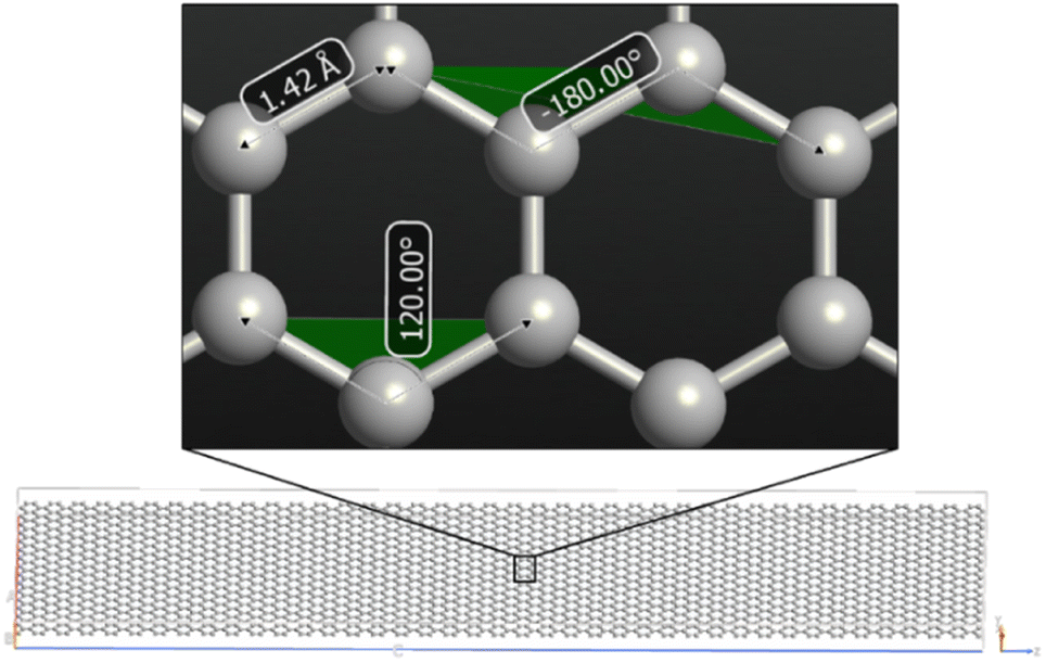 | ||
| Fig. 2 Graphene monolayer with a focus on two rings. | ||
While the bond length is intermediate between a single and a double C–C bond, we found a perfectly conjugated system which allows the electron cloud to be delocalized over ring structures, giving graphene the already known outstanding property of electron mobility and conductivity.
Graphene possesses a zero-band gap and a linear dispersion relation due to massless electrons, and computations confirmed this behavior. In the calculation of the graphene band structure (Fig. 3(A)), seven bands have been reported with different colors in relation to the lowest and highest energy values. The effective mass was calculated considering each band, and values of 0.0008, 0.0009, 0.0011, 0.0021, 0.0016, 0.0009, 0.0039 and 0.0012 were obtained. Moreover, contacts between conduction bands and valences bands were detected in K-points in the Brillouin zone, where we can also observe the Dirac cones (see Fig. 3(A)). Following the Brillouin zone of graphene, six crossing points in the K-points can be detected, which means that we have six Dirac cones, and all of them appear in the six corners of the aromatic ring (Fig. 3(B)).50
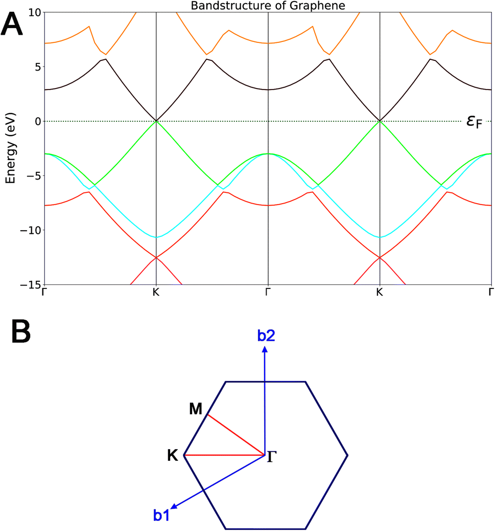 | ||
| Fig. 3 Bandgap structures (A) and Brillouin zone of graphene (B). | ||
In terms of energy, these bands intersect exactly at EF (the Fermi level), which corresponds to the special K-point in the reciprocal space of the hexagonal lattice. In the density of states, the Dirac-cone-like energy bands result in a V-shaped structure with vanishing carrier density at EF; thus, monolayer graphene is a kind of zero-gap semimetal.51
I(V) characteristics of graphene diodes
Next, after the validation step, diodes with dimensions of 15 nm2 along x and z axes were modelled, then three different necks were generated. I(V) property calculations were carried out for these geometrical graphene devices consisting of Graphene-N8, Graphene-N6, and Graphene-N4 at zero gate voltage. The computed results in Fig. 4(A) reveal the non-linear I(V) shapes of all cases in excellent consistency with the experimental measurements of Zhu et al.20 According to the data presented in Fig. 4(A) and Table 1, by decreasing the neck width of the graphene devices from 8 nm to 4 nm, the current values were reduced at positive and negative voltages. Moreover, the amount of current at voltage 0.5 V reduces from 42 μA for Graphene-N8 to 33 μA for Graphene-N6 and 27 μA for Graphene-N4. Similarly, the current values at voltage −0.5 V dropped from 41 μA for Graphene-N8 to 29 μA for Graphene-N6 and 22 μA for Graphene-N4. These values obtained from our quantum simulations for Graphene-N6 are in excellent agreement with experimental outcomes20 (see Table 1) with 35 μA and 30 μA at −0.5 V and 0.5 V, respectively. Conversely, our results follow the same trend as the Monte Carlo simulation in ref. 52 for large-scale geometric graphene diodes with neck widths of 50 nm, 200 nm and 600 nm.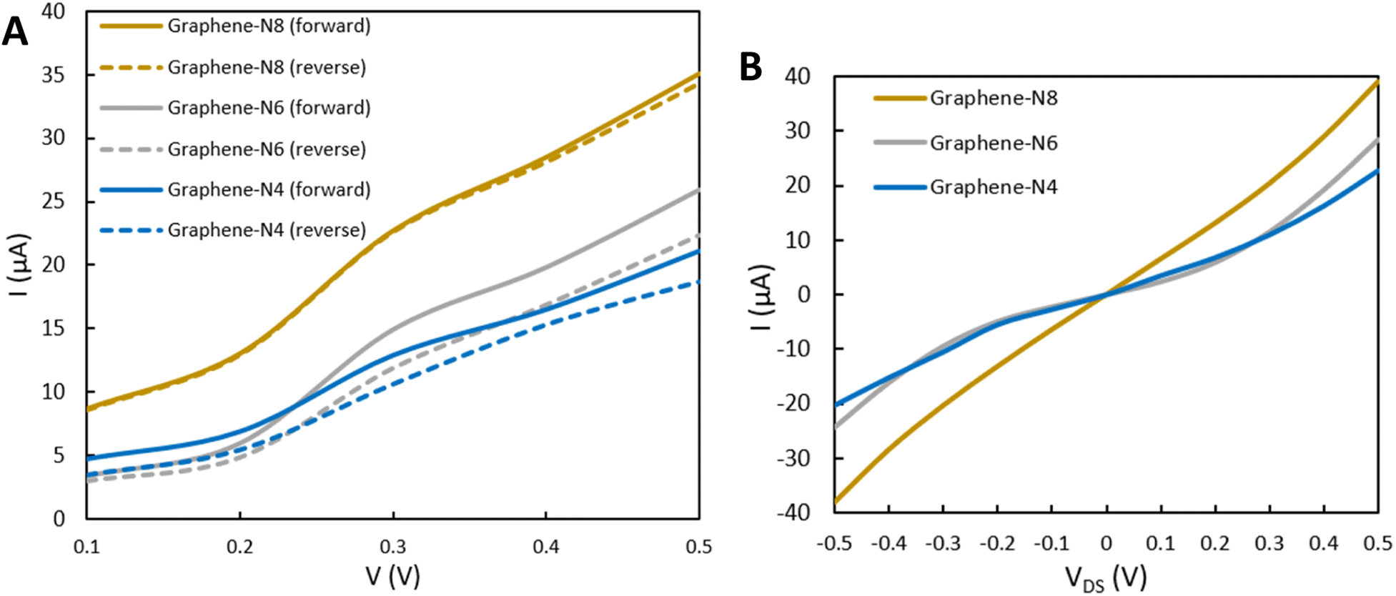 | ||
| Fig. 4 I(V) characteristics of Graphene-N8, Graphene-N6, and Graphene-N4 diodes without applying a gate voltage (A) and with applying a gate voltage at Vg = 20 V and ε = 3.9 (B). VDS refers to the voltage from drain to source and N is the neck of the graphene. | ||
| 1 V | −0.5 V | Device | 0.5 V | −1 V |
|---|---|---|---|---|
| 100 μA | 41 μA | Graphene-N8 | 42 μA | 99 μA |
| 86 μA | 29 μA | Graphene-N6 | 33 μA | 84 μA |
| 72 μA | 22 μA | Graphene-N4 | 27 μA | 60 μA |
| — | 30 μA | Exp.20 | 35 μA | — |
In the next step, we performed quantum simulations for the effect of applying a gate voltage (Vg) of 20 V to the three graphene devices in the presence of the dielectric (ε) in the zone between graphene diodes and the metallic gate (Fig. 1), to observe how an electric field passing from different ε can affect the I(V) characteristic and transport behavior of the graphene diodes. Consistent with experiments,20,25,53Fig. 4(B) reveals asymmetric I(V) properties calculated for Graphene-N8, Graphene-N6, and Graphene-N4 devices with majority charge carriers of electrons and holes at Vg = 20 V and ε = 3.9. Inspection of Table 2 reveals that at higher voltages, Graphene-N8 with high current values of 177 μA and 174 μA slightly overestimates the experimental values of 155 μA and 115 μA at 1.5 V and −1.5 V, respectively, whereas Graphene-N6 gave us a very close current value of 153 μA at voltage 1.5 V with good consistency between experiment and theory. Further, the I(V) characteristics of Graphene-N4 with 111 μA at −1.5 V is in very good agreement with the experimental and theoretical values of 115 μA and 107 μA, respectively. The results reveal that at lower voltages a graphene device with neck width 8 nm showed greater similarity to experiments for the current values, whereas by increasing the bias those devices with shorter necks (Graphene-N6 and Graphene-N4) showed better agreement with measurements in forward and reverse directions of voltage, respectively.
Asymmetry (A)
It is worth mentioning that efficient rectification requires a large forward-to-backward current ratio. This ratio is referred to as the “A ratio” of the diode and some other figures of merit (such as the responsivity) also depend on the A of the I(V) behaviour. More importantly, to confirm the effect of the geometry of graphene on the I(V) curves, as an important difference in the characteristics of geometrically asymmetric graphene diodes with respect to symmetric ones, we quantified the I(V) A ratio for different diodes.54 To analyze the A property of the I(V) characteristics for different diodes, we considered the ratio of the current absolute value at positive (+V) and negative (−V) voltages using the formula asymmetry ratio = |I(+V)/I(−V)|. If A > 1, electron transport is dominant, whereas in the case when A < 1, hole transport is dominant. The data obtained from A are presented in Fig. 5, calculated from the I(V) characteristics of different AGDs under no gate voltage (NGV) and with gate voltage (WGV) conditions. As the results show in the NGV, Graphene-N4 with a smaller neck size achieved the greatest A of 1.39 at voltage |0.1 V|, while Graphene-N6 and Graphene-N8 have their maximum A of 1.20 and 1.03 at higher voltages of |0.22 V| and |0.4 V|, respectively. As shown in Fig. 5, A in lower voltages indicates higher values while by raising the voltage we observed lower amounts of A and some graph convergency.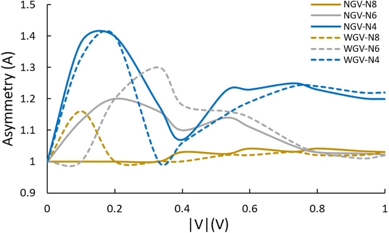 | ||
| Fig. 5 Calculated asymmetry (A) values of graphene devices with different necks of Graphene-N8, Graphene-N6, Graphene-N4 with no gate voltage (NGV (solid lines)) and with gate voltage (WGV (dashed lines)) of 20 V. | ||
By applying a gate voltage (WGV) of +20 V, the A of Graphene-N4 showed a slight increase to 1.40 (Fig. 5, blue dashed line) that was calculated for |V| = 0.2 V. However, the corresponding A for Graphene-N6 and Graphene-N8 were raised to 1.30 and 1.16 at |V| = 0.3 V and |V| = 0.1 V with respect to the NGV system. The results of the AR trend in this study are very consistent with the Monte Carlo simulations in Zhu et al.20 and experimental measurements of Passi et al.20,55 in which the smallest neck device yields a higher A.
Transmission spectra (T)
Modeling of T spectra was performed to compare the ballistic efficiencies of geometric graphene devices as a function of optical properties, quantitively and qualitatively. For a 2D graphene structure, the T spectrum in principle represents just a sum over available modes in the band structure at each energy. As can be seen in Fig. 6, we estimated T spectra for different geometrical graphene devices at bias energies ranging from −2 to +2 eV using a Dirac self-energy calculator, while we fixed the difference in chemical potential between the right and left electrodes at 5 eV. The simulation results from Fig. 6 and Table 3 show that the maximum value of T increases with a decrease in the neck of graphene in various devices, among which Graphene-N4 shows at higher value of T = 6.72 in the energy range 1.30. This simulation indicates that the overall trend of T is in agreement with the A properties of graphene devices, as confirmed by some previous studies.32,56 It is worth noting that the harvesting efficiency of antennas has been discussed by several authors in recent years. While Midrio et al.57 referred to receiving efficiency in antennas, some previously published papers focused on transmission and reflection efficiencies. Recently, in a study by Ma et al.58 the optical efficiency of nano-antenna systems for solar energy harvesting was considered. The maximum upper bounds were found to be in the order of 60–70%. Moreover, Zhao et al.,59 investigated the collection of solar energy by a broad-band antenna to overcome the low efficiency of a solar rectenna based on conventional nano-antennas. The antenna impedance, radiation, polarization and effective area are all considered in efficiency calculations using the finite integral technique. The wavelength range investigated is 300–3000 nm, which corresponds to more than 98% of solar radiation energy. Recently Mencarelli et al.,60 using Monte Carlo simulations, studied the charge transmittivity of geometric diodes based on graphene patterned with spatial asymmetry for a voltage difference of 1.76 V. With fixed external voltage, charge direction is not relevant for transmittivity, owing to reciprocity. However, when a voltage with the opposite sign is considered, the transmittivity changes due to superposition between voltage and asymmetric geometry, so that I(V) asymmetry follows. Clearly, different methodologies from atomistic DFTB to Monte Carlo and experiments cannot calculate the same T property for geometrical graphene diodes; however, each of them can satisfy effective implementation of the concept of a geometric diode for harvesting applications.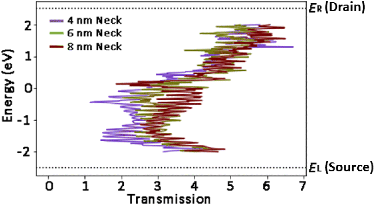 | ||
| Fig. 6 Simulated transmission spectra of Graphene-N8, Graphene-N6, and Graphene-N4 devices. | ||
| Device | Energy (eV) | Max transmittance |
|---|---|---|
| Graphene-N8 | 1.56 | 6.44 |
| Graphene-N6 | 1.52 | 6.16 |
| Graphene-N4 | 1.30 | 6.72 |
Conclusions
In this study, geometric graphene diodes were investigated from the atomic perspective using the first principles DFTB-NEGF method. To this end, three different AGDs consisting of Graphene-N8, Graphene-N6, and Graphene-N4, in the shape of ballistic diodes were modelled with different neck widths. The atomic behavior of the graphene devices was explored through I(V) characteristics, A properties and T spectra. Whereas all simulated AGDs exhibited asymmetric I(V) characteristics in excellent agreement with experimental measurements and Monte Carlo simulation, Graphene-N8 delivers the highest current values at lower and higher voltages under no gate voltage (NGV) and with gate voltage (WGV) conditions. By applying a gate voltage of +20 V, Graphene-N6 and Graphene-N4 showed better agreement with the experimental data for forward and reverse directions of voltage, respectively. The best A was found for Graphene-N4 with a value of 1.40 at a corresponding voltage of |V| = 0.2 with maximum T = 6.72 in an energy range of 1.30 eV. This computational study for optimizing geometrical graphene devices offers a new insight into the development of energy harvesting devices. Furthermore, the accuracy demonstrated by the atomistic approach allowed us to highlight in detail phenomena that could be difficult to interpret with a purely experimental approach, thus suggesting points of focus for the production of promising graphene rectifiers, enabling the realization of optical rectennas.Author contributions
Conceptualization, E. M., E. L. and P. S.; methodology, E. M. and E. L.; validation, E. M., E. L., P. S., L. P. and D. M; investigation, E. M.; data curation, E. M.; writing—original draft preparation, E. M.; writing—review and editing, E. M., E. L., E. P., P. S., L. P., A. H., and D. M.; visualization, E. M.; supervision, P. S.; project administration, E. M., E. L., E. P., P. S., A. H., L. P. and D. M. All authors have read and agreed to the published version of the manuscript.Conflicts of interest
There are no conflicts to declare.Acknowledgements
This work is part of the research of “Wideband optical antennae for use in energy harvesting applications” (GreEnergy) (grant agreement no. 101006963).References
- J. Y. Huang, F. Ding, B. I. Yakobson, P. Lu, L. Qi and J. Li, Proc. Natl. Acad. Sci. U. S. A., 2009, 106(25), 10103–10108 CrossRef CAS PubMed.
- L. Banszerus, M. Schmitz, S. Engels, J. Dauber, M. Oellers, F. Haupt, K. Watanabe, T. Taniguchi, B. Beschoten and C. Stampfer, Sci. Adv., 2015, 1(6), e1500222 CrossRef PubMed.
- C. Lee, X. Wei, J. W. Kysar and J. Hone, Science, 2008, 321, 385–388 CrossRef CAS PubMed.
- A. A. Balandin, S. Ghosh, W. Bao, I. Calizo, D. Teweldebrhan, F. Miao and C. N. Lau, Nano Lett., 2008, 8, 902–907 CrossRef CAS PubMed.
- F. Withers, M. Dubois and A. K. Savchenko, Phys. Rev. B, 2010, 82, 073403 CrossRef.
- M. Liu, X. Yin, E. Ulin-Avila, B. Geng, T. Zentgraf, L. Ju, F. Wang and X. Zhang, Nature, 2011, 474, 64–67 CrossRef CAS PubMed.
- M. Pérez, J. Elías, M. Sosa and M. Vallejo, Eur. J. Phys., 2022, 43, 045401 CrossRef.
- L. Pierantoni, D. Mencarelli and F. Coccetti, in 2013 7th European Conference on Antennas and Propagation (EuCAP), IEEE, 2013, pp. 712–715 Search PubMed.
- Z. X. Wang, Z. Y. Zhang and L. M. Peng, Chin. Sci. Bull., 2012, 57, 2956–2970 CrossRef CAS.
- P. Avouris and C. Dimitrakopoulos, Graphene: Synthesis and Applications, 2012 Search PubMed.
- Y. Qiao, X. Li, T. Hirtz, G. Deng, Y. Wei, M. Li, S. Ji, Q. Wu, J. Jian and F. Wu, Nanoscale, 2019, 11, 18923–18945 RSC.
- A. Nag, A. Mitra and S. C. Mukhopadhyay, Sens. Actuators, A, 2018, 270, 177–194 CrossRef CAS.
- K. I. Bolotin, K. J. Sikes, Z. Jiang, M. Klima, G. Fudenberg, J. Hone, P. Kim and H. L. Stormer, Solid State Commun., 2008, 146, 351–355 CrossRef CAS.
- L. Wang, I. Meric, P. Y. Huang, Q. Gao, Y. Gao, H. Tran, T. Taniguchi, K. Watanabe, L. M. Campos and D. A. Muller, Science, 2013, 342, 614–617 CrossRef CAS PubMed.
- Z. Zhu, S. Joshi, S. Grover and G. Moddel, J. Phys. D: Appl. Phys., 2013, 46, 185101 CrossRef.
- D. Dragoman and M. Dragoman, J. Phys. D: Appl. Phys., 2013, 46, 055306 CrossRef.
- G. Auton, J. Zhang, R. K. Kumar, H. Wang, X. Zhang, Q. Wang, E. Hill and A. Song, Nat. Commun., 2016, 7, 11670 CrossRef CAS PubMed.
- C. W. J. Beenakker and H. Van Houten, Solid State Phys., 1991, 44, 1–228 Search PubMed.
- A. S. Mayorov, R. V. Gorbachev, S. V. Morozov, L. Britnell, R. Jalil, L. A. Ponomarenko, P. Blake, K. S. Novoselov, K. Watanabe, T. Taniguchi and A. K. Geim, Nano Lett., 2011, 11, 2396–2399 CrossRef CAS PubMed.
- Z. Zhu, S. Grover, K. Krueger and G. Moddel, in Conference Record of the IEEE Photovoltaic Specialists Conference, 2011, pp. 002120–002122 Search PubMed.
- D. Mencarelli, G. M. Zampa and L. Pierantoni, IEEE Access, 2022, 10, 123251–123258 Search PubMed.
- A. Hemmetter, X. Yang, Z. Wang, M. Otto, B. Uzlu, M. Andree, U. Pfeiffer, A. Vorobiev, J. Stake and M. C. Lemme, ACS Appl. Electron. Mater., 2021, 3, 3747–3753 CrossRef CAS.
- M. Dragoman and M. Aldrigo, Appl. Phys. Lett., 2016, 109, 113105 CrossRef.
- A. Rogalski, Prog. Quantum Electron., 2003, 27, 59–210 CrossRef CAS.
- G. Moddel, Z. Zhu, S. Grover and S. Joshi, Solid State Commun., 2012, 152, 1842–1845 CrossRef CAS.
- M. N. Gadalla, M. Abdel-Rahman and A. Shamim, Sci. Rep., 2014, 4, 1–9 Search PubMed.
- J. Brownless, J. Zhang and A. Song, Carbon, 2020, 168, 201–208 CrossRef CAS.
- A. K. Singh, G. Auton, E. Hill and A. Song, Carbon, 2015, 84, 124–129 CrossRef CAS.
- P. T. Landsberg and G. Tonge, J. Phys. A: Math. Gen., 1979, 12, 551 CrossRef.
- M. Buttiker, J. Phys.: Condens. Matter, 1993, 5, 9361 CrossRef CAS.
- T. Christen and M. Büttiker, Europhys. Lett., 1996, 35, 523 CrossRef CAS.
- V. H. Nguyen, D. C. Nguyen, S. Kumar, M. Kim, D. Kang, Y. Lee, N. Nasir, M. A. Rehman, T. P. A. Bach, J. Jung and Y. Seo, npj 2D Mater. Appl., 2021, 5, 89 CrossRef CAS.
- G. Seifert, H. Eschrig and W. Bieger, Zeitschrift Fur Physikalische Chemie-Leipzig, 1986, 267, 529–539 CAS.
- W. M. C. Foulkes and R. Haydock, Phys. Rev. B, 1989, 39, 12520 CrossRef PubMed.
- M. Elstner, D. Porezag, G. Jungnickel, J. Elsner, M. Haugk, T. Frauenheim, S. Suhai and G. Seifert, Phys. Rev. B, 1998, 58, 7260 CrossRef CAS.
- E. Mohebbi, E. Pavoni, L. Pierantoni, P. Stipa, E. Laudadio and D. Mencarelli, in 2023 IEEE 23rd International Conference on Nanotechnology (NANO), IEEE, 2023, pp. 238–242 Search PubMed.
- Z. Wan, Q. De Wang, D. Liu and J. Liang, Comput. Mater. Sci., 2021, 198, 110699 CrossRef CAS.
- E. Mohebbi, E. Pavoni, D. Mencarelli, P. Stipa, E. Laudadio and L. Pierantoni, Front. Mater., 2023, 10, 1145822 CrossRef.
- N. R. Papior, G. Calogero and M. Brandbyge, J. Phys.: Condens. Matter, 2018, 30, 25LT01 CrossRef PubMed.
- E. Mohebbi, E. Pavoni, D. Mencarelli, P. Stipa, L. Pierantoni and E. Laudadio, Nanoscale Adv., 2022, 4, 3634–3646 RSC.
- M. J. van Setten, M. Giantomassi, E. Bousquet, M. J. Verstraete, D. R. Hamann, X. Gonze and G. M. Rignanese, Comput. Phys. Commun., 2018, 226, 39–54 CrossRef CAS.
- S. Smidstrup, T. Markussen, P. Vancraeyveld, J. Wellendorff, J. Schneider, T. Gunst, B. Verstichel, D. Stradi, P. A. Khomyakov, U. G. Vej-Hansen, M. E. Lee, S. T. Chill, F. Rasmussen, G. Penazzi, F. Corsetti, A. Ojanperä, K. Jensen, M. L. N. Palsgaard, U. Martinez, A. Blom, M. Brandbyge and K. Stokbro, J. Phys.: Condens. Matter, 2020, 32, 015901 CrossRef CAS PubMed.
- J. H. Ammeter, H.-B. Bürgi, J. C. Thibeault and R. Hoffmann, J. Am. Chem. Soc., 1978, 100(12), 3686–3692 CrossRef CAS.
- H. Eschrig, Optimized LCAO Method and the Electronic Structure of Extended Systems, Walter de Gruyter GmbH & Co KG, 2022 Search PubMed.
- K. Stokbro, D. E. Petersen, S. Smidstrup, A. Blom, M. Ipsen and K. Kaasbjerg, Phys. Rev. B, 2010, 82, 075420 CrossRef.
- T. Ozaki, K. Nishio and H. Kino, Phys. Rev. B, 2010, 81, 035116 CrossRef.
- E. Pavoni, E. Mohebbi, P. Stipa, L. Pierantoni, D. Mencarelli, M. Dragoman, M. Aldrigo and E. Laudadio, Nanoscale Adv., 2023, 5, 2748–2755 RSC.
- G. M. Zampa, D. Mencarelli and L. Pierantoni, Phys. B, 2023, 661, 414917 CrossRef CAS.
- H. Haug and A.-P. Jauho, Quantum Kinetics in Transport and Optics of Semiconductors, Springer, 2008, vol. 2 Search PubMed.
- L. Pierantoni, N. Pelagalli, D. Mencarelli, A. Di Donato, M. Orlandini, J. Pagliuca and T. Rozzi, Appl. Sci. (Switzerland), 2021, 11, 1–13 Search PubMed.
- X. L. Wang, S. X. Dou and C. Zhang, NPG Asia Mater., 2010, 2, 31–38 CrossRef.
- Z. Zhu, S. Joshi and G. Moddel, IEEE Journal on Selected Topics in Quantum Electronics, 2014, 20, 70–78 Search PubMed.
- Z. Zhu, S. Joshi, S. Grover and G. Moddel, Rectenna Solar Cells, 2013, 209–227 CAS.
- E. Pavoni, E. Mohebbi, P. Stipa, L. Pierantoni, D. Mencarelli, M. Dragoman, M. Aldrigo and E. Laudadio, Nanoscale Adv., 2023, 5, 2748–2755 RSC.
- V. Passi, A. Gahoi and M. C. Lemme, in 2017 Silicon Nanoelectronics Workshop (SNW), IEEE, 2017, pp. 137–138 Search PubMed.
- J. P. Custer Jr, J. D. Low, D. J. Hill, T. S. Teitsworth, J. D. Christesen, C. J. McKinney, J. R. McBride, M. A. Brooke, S. C. Warren and J. F. Cahoon, Science, 2020, 368, 177–180 CrossRef PubMed.
- M. Midrio, L. Pierantoni, S. Boscolo, D. Truccolo and D. Mencarelli, Opt. Express, 2022, 30, 7017–7034 CrossRef CAS PubMed.
- Z. Ma and G. A. E. Vandenbosch, Sol. Energy, 2013, 88, 163–174 CrossRef CAS.
- H. Zhao, H. Gao, T. Cao and B. Li, Opt. Express, 2018, 26, A178–A191 CrossRef CAS PubMed.
- D. Mencarelli, G. M. Zampa and L. Pierantoni, IEEE Access, 2022, 10, 123251–123258 Search PubMed.
| This journal is © The Royal Society of Chemistry 2024 |