
 Open Access Article
 This Open Access Article is licensed under a Creative Commons Attribution-Non Commercial 3.0 Unported Licence
Adjusting surface coverage of Pt nanocatalyst decoration for selectivity control in CMOS-integrated SnO2 thin film gas sensors†
F.
Sosada-Ludwikowska
a,
L.
Reiner
a,
L.
Egger
a,
E.
Lackner
a,
J.
Krainer
a,
R.
Wimmer-Teubenbacher
a,
V.
Singh
 b,
S.
Steinhauer
c,
P.
Grammatikopoulos
*de and
A.
Koeck
a
b,
S.
Steinhauer
c,
P.
Grammatikopoulos
*de and
A.
Koeck
a
aMaterials Center Leoben Forschung GmbH, 8700, Leoben, Austria
bNanoparticles by Design Unit, Okinawa Institute of Science and Technology (OIST), Graduate University, 904-0495, Okinawa, Japan
cDepartment of Applied Physics, KTH Royal Institute of Technology, 106 91 Stockholm, Sweden
dMaterials Science and Engineering, Guangdong Technion – Israel Institute of Technology, Shantou, Guangdong 515063, China. E-mail: panagiotis.g@gtiit.edu.cn
eGuangdong Provincial Key Laboratory of Materials and Technologies for Energy Conversion, Guangdong Technion – Israel Institute of Technology, Shantou, Guangdong 515063, China
First published on 15th January 2024
Abstract
Smart gas-sensor devices are of crucial importance for emerging consumer electronics and Internet-of-Things (IoT) applications, in particular for indoor and outdoor air quality monitoring (e.g., CO2 levels) or for detecting pollutants harmful for human health. Chemoresistive nanosensors based on metal-oxide semiconductors are among the most promising technologies due to their high sensitivity and suitability for scalable low-cost fabrication of miniaturised devices. However, poor selectivity between different target analytes restrains this technology from broader applicability. This is commonly addressed by chemical functionalisation of the sensor surface via catalytic nanoparticles. Yet, while the latter led to significant advances in gas selectivity, nanocatalyst decoration with precise size and coverage control remains challenging. Here, we present CMOS-integrated gas sensors based on tin oxide (SnO2) films deposited by spray pyrolysis technology, which were functionalised with platinum (Pt) nanocatalysts. We deposited size-selected Pt nanoparticles (narrow size distribution around 3 nm) by magnetron-sputtering inert-gas condensation, a technique which enables straightforward surface coverage control. The resulting impact on SnO2 sensor properties for CO and volatile organic compound (VOC) detection via functionalisation was investigated. We identified an upper threshold for nanoparticle deposition time above which increased surface coverage did not result in further CO or VOC sensitivity enhancement. Most importantly, we demonstrate a method to adjust the selectivity between these target gases by simply adjusting the Pt nanoparticle deposition time. Using a simple computational model for nanocatalyst coverage resulting from random gas-phase deposition, we support our findings and discuss the effects of nanoparticle coalescence as well as inter-particle distances on sensor functionalisation.
1 Introduction
Over the past decades, the physicochemical properties of metal-oxide nanostructures have been extensively studied, aiming at diverse applications including solar cells, photonic devices, batteries, (photo-) catalysts, and sensors.1 Among the latter, gas sensors relying on resistive transduction principles (conductometric gas sensors) have been successfully developed and commercialised, featuring capabilities for highly sensitive target analyte detection in the parts-per-million (ppm) or parts-per-billion (ppb) range.2 The most promising use cases are indoor and outdoor air quality monitoring of toxic or harmful gases3 and personalised healthcare applications4 such as breath analysis for disease diagnostics.5 To meet the requirements of these applications and to penetrate consumer electronics markets, metal-oxide gas sensor technologies need to be suitable for scalable low-cost production and for operation at low power consumption (in addition to fulfilling often stringent gas sensitivity and selectivity demands). In this regard, device miniaturisation and integration with complementary metal-oxide semiconductor (CMOS) technology, in particular combining the gas sensitive metal-oxide materials with microhotplate (μhp) structures,6 are successful strategies towards realising gas sensor devices compatible with wearables or distributed sensor networks for Internet-of-Things (IoT) applications.The most common metal-oxide semiconductors employed in gas sensor devices are SnO2,3 ZnO,7 CuO,8 and WO3.9 The implementation of nanomaterials such as nanocrystalline thin films, nanowires, or nanoparticles ensures high gas-sensitivity via maximising the surface-to-volume ratio. However, selectivity, i.e., the capability of the sensor to distinguish between different target analytes, remains insufficient in most cases, which constitutes a major hindrance for the broad applicability of conductometric gas sensors. This lack of selectivity is a result of metal oxides typically reacting with multiple gas species, resulting in non-specific changes in conductivity. Various approaches for selectivity improvements have been reported, in particular by tailoring the employed materials via catalyst decoration, composite/heterostructure formation or surface functionalisation10,11 and by dynamic operation modes such as temperature cycling.12 In addition to selectivity enhancements, decoration/functionalisation with other nanomaterials can improve sensitivity and lower the device operation temperature.13
In this study, we report on CMOS-integrated SnO2 thin film gas sensors on miniaturised μhp devices and their decoration with size-selected Pt nanocatalysts. Nanocrystalline SnO2 gas sensitive layers were fabricated by an efficient, low-cost spray pyrolysis process at atmospheric pressure. Pt sensitisation was performed via the deposition of pre-formed nanoparticles by means of magnetron-sputtering inert-gas condensation – a versatile gas-phase method for the synthesis of nanoparticles with tuneable size, chemical composition, and morphology.14,15 The effectiveness of this technique for realising high-performance conductometric gas sensors has been previously demonstrated for sensing layers based on Fe nanoparticles with well-defined cubic shapes,16 for Pd nanoparticle-decorated CuO nanowire devices,17 and for Ru nanoparticle-decorated CuO nanowire devices.18 Recently, we demonstrated the decoration of SnO2 thin films with ultrasmall Pt nanoparticles with an average diameter below 2 nm, resulting in carbon monoxide (CO) sensitivity with minimised humidity interference.19
Additional investigations in this direction are important for further demonstrating the suitability of our CMOS-integrated approach in more complex gas environments. Here, we studied SnO2 thin films decorated with size-selected Pt nanocatalysts exhibiting an average diameter around 3 nm for the cases of CO and volatile organic compound (VOC) detection. Sensing low CO concentrations is of immediate relevance as this gas is a toxic environmental pollutant produced in industrial, automotive, and domestic combustion of fuels.20 In a similar way, VOC detection is highly important to assess exposure to these potentially toxic, carcinogenic, and mutagenic gases, typically occurring in domestic, industrial, and transportation scenarios.21 Our CMOS-integrated gas sensors showed consistently excellent performance in the low ppm range at different relative humidity levels. For different Pt coverages and operation temperatures, non-trivial dependency of gas selectivity between CO and VOCs was observed, providing guidance for indoor air quality, environmental monitoring, industrial, and health applications,22 where such gas selectivity is highly relevant. For instance, in measurements of poor indoor air quality due to VOCs from human respiration and perspiration, often linked with the sick building syndrome, CO constitutes a common interferent gas from pollutant sources such as stoves and heaters.23 Our experimental findings were juxtaposed with those of a basic computational model for nanoparticle deposition, introduced here in order to elucidate the effect of nanoparticle ripening and inter-particle distances as a function of deposition time (which directly corresponds to coverage). Based on these findings, we elaborate on the different contributions of electronic and chemical device sensitisation.
2 Experimental
2.1 Fabrication of CMOS-integrated micro-hotplate chips for SnO2 sensing films
A chemical sensor platform based on 0.35 μm standard CMOS technology and backend processing was employed within this study, comprising an array of 8 μhps for a total of 16 chemical sensors on a single chip.19 The optimised μhps24 relied on a poly-Si heater and were patterned by etching through the CMOS stack down to the bulk Si. The backend processing included a photolithography step, followed by evaporation of Ti/Pt (5 nm/150 nm) and a lift-off process to fabricate the electrodes, which were designed for contacting the gas sensitive layer in 4-point configuration on the μhps. Afterwards, the wafer was diced into 2 × 2 cm2 sized chips and gas-sensitive SnO2 thin films (thickness 50 nm) were deposited by using spray pyrolysis technology at atmospheric pressure. The chips were placed on a hotplate at a temperature of 400 °C; then a solution of tin chloride pentahydrate (SnCl4·5H2O) in ethyl acetate as precursor material was sprayed onto the chips by an atomising nozzle using N2 as carrier gas.25 Subsequently, the SnO2 thin film was annealed by placing the whole CMOS chip on a hotplate at 400 °C for 60 min. Then a photolithography process step followed by Ar-ion etching was performed for patterning the gas-sensitive SnO2 films. Another photolithography step was employed to coat the SnO2 sensing films with a resist protection layer before the μhps were under-etched by an isotropic XeF2 dry-etching process. This was followed by a cleaning process to remove the resist protection layer from the sensing films. The fabrication steps are illustrated in the schematics of Fig. 1a, and a scanning electron microscopy (SEM) image of a typical device is shown in Fig. 1b. In a final step, the 2 × 2 cm2 sized chips were processed by stealth dicing into single dies (4.7 × 5.1 mm2), which were glued and wire-bonded to printed circuit boards for the gas measurements.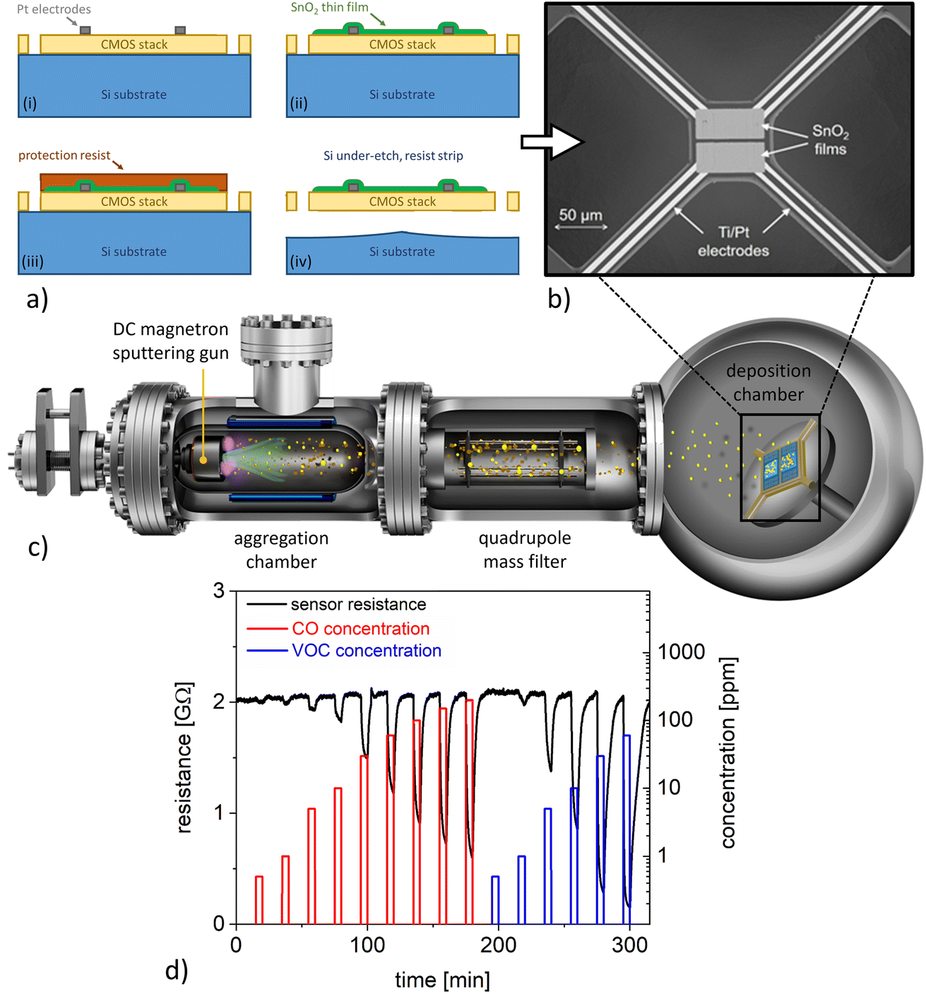 | ||
| Fig. 1 (a) Fabrication steps for the realisation of CMOS-integrated SnO2 thin films sensors. (b) Scanning electron microscopy image of typical device. The sensor structure is integrated on a suspended microhotplate mechanically connected via four arms. (c) Schematic of sensor functionalisation via magnetron-sputtering inert-gas condensation. (d) Chemoresistive signal of a pristine SnO2-based gas sensor at 50% relative humidity and an operation temperature of 200 °C. | ||
2.2 Functionalisation of CMOS-integrated SnO2 thin film sensors with Pt nanoparticles
The single sensor dies were decorated with Pt nanoparticles by magnetron-sputtering inert-gas condensation in a high-vacuum deposition system (Mantis Deposition Ltd, UK), employing a cluster beam source and an in-line quadrupole mass filter (QMF) for size selection (Fig. 1c).14 The base pressure was ∼10−8 mbar before deposition, whereas the pressures were ∼10−4 mbar and ∼10−1 mbar in the main chamber and in the aggregation zone, respectively, during NP deposition. The substrate holder was rotated at 2 rpm for ensuring homogeneous nanoparticle surface coverage. Pt nanoparticles with an average diameter of 3 nm were deposited using a magnetron power of 7 W and a constant flow of 70 sccm Ar; the cluster source aggregation length was 100 mm. TEM grids and Si substrates were decorated with Pt nanoparticles using the same parameters, which enabled further characterisation of the size, structure, and surface coverage of the employed nanocatalysts. Three different deposition times of 10 min, 20 min, and 30 min were employed to study the influence of the nanoparticle surface coverage on the sensor response.The size and crystalline structure of Pt nanoparticles were analysed with a FEI Titan G2 Environmental TEM equipped with a spherical aberration image corrector (operation voltage 300 kV). Size distributions were obtained from low-magnification TEM micrographs by means of automated image analysis with the software ImageJ, measuring projected areas and assuming spherical geometries. AFM measurements were performed on Si substrates (roughness ∼0.2 nm root mean square, rms) with Pt nanoparticles using a Multimode 8 instrument (Bruker, CA) in tapping mode.
2.3 Sensor characterisation of bare and Pt nanoparticle-functionalised CMOS-integrated devices
The performance of CMOS-integrated sensors was investigated in an automated measurement setup, which enabled precise control of the gaseous environment. For the sensing measurements, humidified synthetic air at three relative humidity levels (25%, 50%, and 75%; at 20 °C) was employed as background gas, whereas pulses of CO and VOC test gases were introduced at ppm-level concentrations. The VOC test gas consisted of a hydrocarbon gas mixture (=HCmix) of acetylene, ethane, ethene, and propene. Both test gases, CO and HCmix, were ready-to-use mixtures diluted in nitrogen from the company Linde Gas. The μhp devices were operated at a constant temperature by DC-biasing the resistive heater (power consumption 13.5 mW at 400 °C).24 Sensor characterisation was performed at a constant total gas flow of 1000 sccm and at operating temperatures of 200 °C and 350 °C. The relative resistance changes due to the interaction with the test gas (i.e., the sensor response S) was calculated according to S = (Rair − Rgas)/Rair, where Rgas is the sensor resistance in the presence of the test gas and Rair is the sensor resistance in pure synthetic air.3 Results and discussion
Single μhp devices (Fig. 1b) feature a design based on a suspended square (size 74 × 74 μm2) realised via Si under-etching to ensure thermal insulation from the rest of the CMOS chip. The resistive heater and the thermocouple are embedded within the central square, which is mechanically connected by four arms (length 150 μm, width 12 μm) to the rest of the chip. The SnO2 thin film sensors showed sensing responses characteristic for metal oxide-based chemoresistive sensors operated at constant temperatures. Representative sensor signals for CO and VOC detection at 50% relative humidity are presented in Fig. 1d. In both cases, exposure to the target analyte resulted in a decrease of SnO2 resistance, which is commonly observed for n-type metal oxides interacting with reducing gases. The lowest detected concentrations were 0.5 ppm and 1 ppm for CO and VOCs, respectively, which is well below commonly suggested exposure limits.26 However, the sensor responses were dependent on relative humidity level (to be discussed in more detail below) and the signal transients during CO and VOC detection were widely non-selective with similar time constants. These shortcomings motivate further investigations on how to tailor the sensitivity and selectivity of the SnO2 thin films.The functionalisation of SnO2 nanomaterial-based chemical sensors with Pt nanocatalysts has been previously identified as a most promising strategy to realise high-performance devices.27–29 Here, we utilised magnetron-sputtering inert-gas condensation for the deposition of size-selected Pt nanoparticles on the CMOS-integrated SnO2 sensing layers. Our solvent-free gas-phase synthesis approach minimises extrinsic contamination and allows for excellent control over nanoparticle morphology as well as surface coverage. The latter can be achieved in a straightforward manner via adjusting the deposition time. In short, magnetron-sputtering inert-gas condensation can be described as follows (Fig. 1c): atoms of the target material are sputtered by a plasma process and form clusters after cooling down to temperatures suitable for bond formation, which is achieved through collisions with Ar atoms in the gas phase.30 The nanoparticles are deposited onto the sample in the soft-landing regime, which minimises damage to both the nanoparticles and the substrate due to the impact during decoration.31 Due to this room temperature process with minimum impact energy, it can be expected that nanoparticle deposition does not have a major influence on the SnO2 film structure, including crystallography and defects, which are decisive for the overall sensing properties.32 The nanoparticles resulting from cluster growth and coalescence are transported towards the sample by means of a pressure differential between the aggregation zone and the deposition chamber, passing through the QMF, which allows filtration according to their sizes.14
The morphology of the Pt nanocatalysts employed in this study was characterised by TEM imaging and AFM measurements. High-resolution TEM micrographs of selected nanoparticles are presented in Fig. 2a. Well-defined crystalline structures were found with the nanoparticles being commonly delimited by extended facets of (111) and (100) surfaces, which can be explained in terms of Pt surface energies33 and thermodynamic equilibrium shape considerations.34 It can be expected that the specific surface faceting will have an impact on the resulting catalytic activity during exposure to reactive gaseous species.35 In some cases twinned nanoparticles were observed, as shown in the centre panel of Fig. 2a. Nanoparticle size distributions were evaluated using TEM imaging combined with automated image analysis (Fig. 2b). An average nanoparticle diameter around 3 nm was found (assuming circular morphologies), which is in good agreement with the values obtained from AFM measurements (ESI Fig. S1†) and from the in-line QMF during nanoparticle deposition (not shown here).
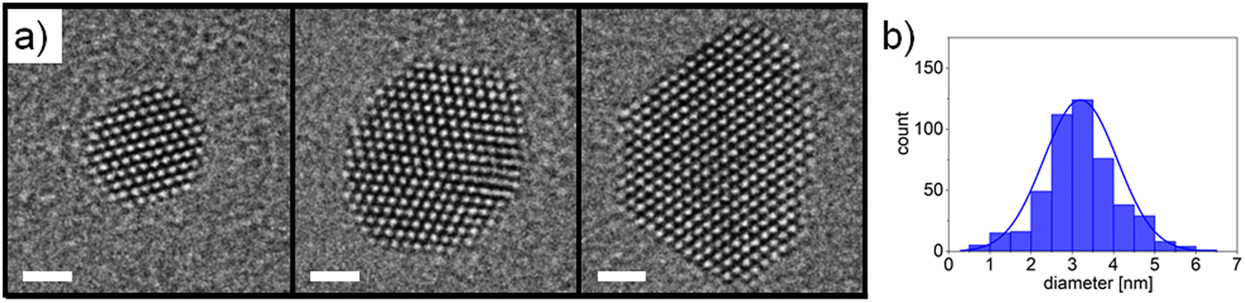 | ||
| Fig. 2 (a) High-resolution TEM micrographs of Pt nanoparticles, showing crystalline structure and surface faceting (scale bars: 1 nm). (b) Size distribution of Pt nanoparticles (normal distribution) obtained by TEM imaging and automated image analysis, assuming circular nanoparticle diameters. | ||
As mentioned above, magnetron-sputtering inert-gas condensation allows for precise control of nanoparticle surface coverage via adjusting the deposition time. After having established the desired deposition parameters, TEM characterisation at low magnification allows for evaluating the areal density of Pt nanoparticles (μm−2) and/or the ratio of covered surface area. In the presented case, we utilised deposition times of 10 min, 20 min, and 30 min (see representative examples in Fig. 3). A deposition time of 10 min corresponded to a nanoparticle areal density of 6600 μm−2 and around 3% surface coverage. Considering the relative material composition, this would correspond to ∼1% vol. and ∼3% wt. Pt/SnO2 ratio (determined by the ratio of Pt nanoparticle mass calculated from TEM analysis over the SnO2 thin film mass calculated via its bulk density and thickness). Note that the presented case does not correspond to a homogeneous composite bulk material as often reported in literature for thick film sensors. Most examples for SnO2 and SnO2/Pt-based sensors rely on functional materials that show a certain degree of porosity, and noble metal functionalisation is performed via methods such as precipitation and impregnation.36–38 While such porous configurations can be beneficial in terms of sensing properties, we study compact SnO2 thin film layers25 with Pt nanoparticles at the uppermost surface due the advantages of the presented synthesis methods in terms of allowing CMOS integration (limited thermal budget), scalability, and miniaturisation potential. For the cases of 20 min and 30 min deposition time, we determined nanoparticle densities (surface coverages, mass compositions) of 10![[thin space (1/6-em)]](https://www.rsc.org/images/entities/char_2009.gif) 400 μm−2 (6% surface coverage, 6% wt. Pt/SnO2) and 10100 μm−2 (9% surface coverage, 9% wt. Pt/SnO2). The low magnification TEM micrograph shows that, while a large number of nanocatalysts were deposited as isolated nanoparticles, coalescence of clusters was also observed. As a result, the nanoparticle areal densities were similar for the 20 min and 30 min cases due to increased tendency for coalescence with deposition time. The latter is mostly attributed to coalescence at the surface of the support during prolonged deposition, although a contribution from in-flight coalescence cannot be completely excluded. In either case, nanoparticle coalescence can have an effect on the resulting catalytic activity and surface functionalisation, which is considered in the discussion below.
400 μm−2 (6% surface coverage, 6% wt. Pt/SnO2) and 10100 μm−2 (9% surface coverage, 9% wt. Pt/SnO2). The low magnification TEM micrograph shows that, while a large number of nanocatalysts were deposited as isolated nanoparticles, coalescence of clusters was also observed. As a result, the nanoparticle areal densities were similar for the 20 min and 30 min cases due to increased tendency for coalescence with deposition time. The latter is mostly attributed to coalescence at the surface of the support during prolonged deposition, although a contribution from in-flight coalescence cannot be completely excluded. In either case, nanoparticle coalescence can have an effect on the resulting catalytic activity and surface functionalisation, which is considered in the discussion below.
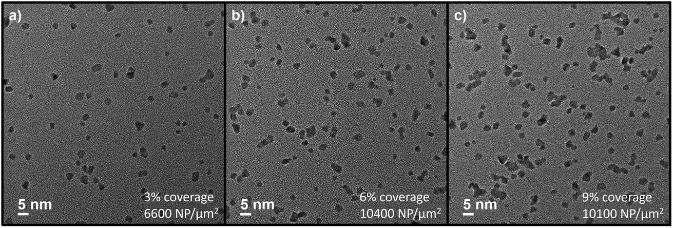 | ||
| Fig. 3 Low-magnification TEM micrographs of Pt nanoparticles deposited for (a) 10 min, (b) 20 min, and (c) 30 min. | ||
For gas sensing characterisation of the investigated devices, we focused on ppm-level CO and VOC concentrations at relative humidity levels between 25% and 75%, which is relevant for practical applications in ambient atmosphere. The CO response of pristine and Pt-decorated SnO2 sensors was assessed at constant operation temperatures of 200 °C and 350 °C (Fig. 4, left; ESI Fig. S2,† top). At 200 °C, we found that the device with 10 min Pt nanoparticle deposition had the highest response S, followed by the pristine SnO2 sensor. The enhancement of the CO signal was up to a factor of two. On the other hand, devices with 20 min and 30 min Pt nanoparticle deposition times showed markedly lower sensor response. For the case of 350 °C, the differences between the four types of sensors in terms of CO signal magnitude were not as pronounced, with the 10 min Pt nanoparticle deposition device again showing the highest response. In comparison, different trends were observed for the VOC sensor responses (Fig. 4, centre; ESI Fig. S2,† bottom). At 200 °C, we found the highest response S for the pristine SnO2 case, while S decreased monotonically with increasing Pt nanoparticle deposition time. Conversely, at 350 °C we observed comparable VOC response for the pristine, 10 min and 20 min case, whereas the 30 min Pt nanoparticle deposition sensor displayed significantly lowered response. Our results are compared to literature reports on CO and VOC sensors in ESI Tables S1 and S2.† The presented devices provide a unique combination of CMOS integration and high hotplate heating efficiency with low detection limits for both CO and VOC target gases, relying on a Pt deposition method that allows for the deposition of size-selected nanocatalysts with excellent coverage control. Compared to other Pt-loaded SnO2-based devices (also considering non-miniaturised and porous film structures), our sensors utilise similar Pt/SnO2 content and show competitive performance.
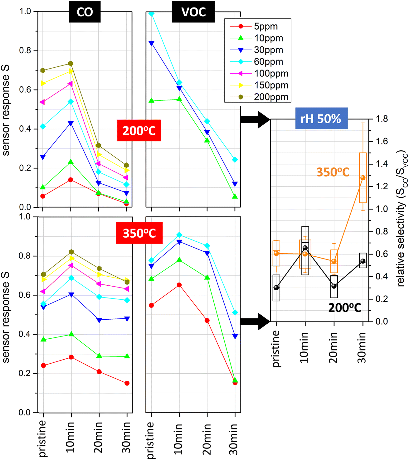 | ||
| Fig. 4 Sensor response S to CO (left) and VOC (right) of pristine and Pt-decorated SnO2 sensors (nanoparticle deposition times 10 min, 20 min, 30 min) at 50% relative humidity (rH) and operation temperatures of 200 °C (top row) and 350 °C (bottom row). The relative selectivity (averaged in the concentration range 5–60 ppm) of CO response over VOC response is shown in the right graph. | ||
It has to be noted that the presence of Pt should have an impact on the humidity dependence of the sensing response.19,39,40 In our previous work19 we observed a monotonous decrease of the sensitivity for increasing relative humidity for the case of pristine SnO2 and significantly lowered humidity interference with ultrasmall Pt nanoparticles (diameter around 1.5 nm). In contrast, the devices presented here show a more complex humidity dependence, which we attribute to the presence of Pt electrodes acting in an analogous manner as Pt nanoparticles but via secondary reactions. Minimised humidity interference is particularly observed for sensors decorated with Pt nanoparticles for 20 min and 30 min (ESI Fig. S2†). In general, such a behaviour is highly beneficial for operation in ambient air with varying humidity.
The presented results of pristine and Pt-decorated SnO2-based sensors show complex correlations between surface coverage, sensor response, humidity cross-sensitivity, as well as differences between the detection of CO and VOCs. Before rationalising these findings, we used a simple computational model (ESI Section B†) to obtain further intuition regarding the effect of nanoparticle coverage/coalescence (or lack of) on inter-particle distances as a function of deposition time, aiming to facilitate the interpretation of our results in terms of chemical and/or electronic sensitisation.
Purposefully designing our model to consist of immobile theoretical “nanoparticles”, we observed a marked difference in coverage levels where the number of theoretical and experimental nanoparticles is maximised between our model and experiment. This deviation can be attributed to differences in mobility between the two particle types. In contrast to their theoretical counterparts, our experimental nanoparticles could roam on the support as a result of their soft-landing; they were neither immersed in the support nor deformed upon deposition (which could increase their interfacial area and, hence, bind them strongly with the support at the landing spot). Their mobility was further assisted by higher temperatures, and availed coalescence with one another. In doing so, the number of isolated particles or particle aggregates dropped earlier than that of the theoretical ones; it is reasonable that the number of their catalytically active sites is also expected to follow suit. At the same time, the area of the depleted region in the support may also be affected, leading to a non-monotonous sensitivity response to coverage.
It should be noted that a different behaviour is expected for the ultrasmall Pt nanoparticles studied previously.19 In that case, heating to 350 °C brought the nanoparticles at (or very near) their size-dependent melting point, forcing them to deform and wet the support, rendering them immobile. In contrast, Pt nanoparticles 3 nm in diameter have a much higher melting point (>725 °C),41 so that such effects should be significantly less pronounced. Finally, considering the high cohesive energy of platinum,42 Ostwald ripening is a less likely mechanism, which may be only auxiliary to this effect.
To conclude, the considerable enhancements related to CO versus VOC selectivity are a result of the Pt nanoparticle coverage control (Fig. 4, right). Our experimental results show that pristine SnO2 sensors operated at 200 °C are highly favourable for VOC detection, as opposed to devices with ∼9% Pt nanoparticle coverage operated at 350 °C, which show superior performance for CO detection. At 200 °C, sensors with ∼3% Pt coverage can be utilised to boost the CO sensing response by about a factor of 2, although the VOC selectivity remains lower compared to the pristine case. When comparing the different Pt loadings, we observe up to twofold changes of sensor selectivity, which can be useful for sensor array configurations such as those described in ref. 23. The CO/VOC selectivity values between 0.2 and 1.2 are consistent with CO selectivity to common VOCs in most previous literature reports on Pt-decorated SnO2-based sensors (ESI Table S2†). Notably, higher CO selectivity up to ∼10 has been shown for screen-printed devices relying on hydrothermally synthesised SnO2 nanoneedles with Pt incorporated into the SnO2 matrix.43 It would be an interesting subject for future studies to investigate further strategies for tailoring CO/VOC selectivity in our SnO2 thin film system, e.g., a comparison of different Pt loading methods to achieve Pt-doped SnO2 material in an analogous manner.
The selectivity values presented here were averaged from 5–60 ppm, which should reflect realistic scenarios with varying analyte concentrations. We observed typical trends of larger CO/VOC selectivity for higher analyte concentrations and, as a consequence, increased error bars for this kind of data evaluation. Such a concentration dependence of selectivity certainly would need to be taken into account in a practical sensor use case. Concentration ranges for the previously mentioned indoor VOC monitoring application in the presence of CO interference from stoves and heaters can be around 10 ppm for CO44 and several ppm for highly variable VOC exposure situations.45
From a sensing mechanism point-of-view, it is obvious that Pt nanoparticles on the SnO2 surface impact the CO and VOC reaction pathways in different ways. SnO2 surface depletion of electrons is a result of both Pt–SnO2 interfaces as well as enhanced oxygen dissociation at the nanocatalyst surfaces, followed by oxygen ionosorption.46 Detection of CO is favoured by a low Pt nanoparticle coverage, interpreted as the configuration where the optimum balance between Pt area and availability of ionosorbed oxygen on the SnO2 surface is reached. Within the framework of reactions with ionosorbed oxygen species, the reaction pathways of CO and VOCs are expected to differ in terms of the number of involved oxygen species involved, i.e., one (multiple) ionosorbed oxygen for CO (VOCs).47 While such a picture may be simplifying, it illustrates how differences in CO/VOC selectivity can be rationalised. In both cases, we expect a complex interplay between various Pt sensitisation mechanisms, including chemical sensitisation (reaction shifted to the Pt surfaces, activated oxygen sites at the SnO2–Pt interface, and oxygen spillover effects) as well as electronic sensitisation.48
Due to the differences in CO and VOC surface reactions, the related reception and transduction processes are favoured at different Pt loadings. At 200 °C and intermediate VOC concentrations, the decoration with Pt nanoparticles decreases the sensor response for increasing loadings, suggesting that the available SnO2 surface area (inversely proportional to Pt coverage) plays an important role. Conversely, at 350 °C the VOC response has a maximum at 10 min Pt deposition, which could be a result of a change in prevailing transduction mechanism. The CO response, on the other hand, peaks for 10 min Pt deposition at both operation temperatures, indicating that the effects of functionalisation dominate here. These characteristics can be linked with well-dispersed Pt nanoparticles (non-agglomerated with size distribution around 3 nm) and inter-particle distances around 9 nm (see ESI Fig. S3a†). At higher Pt loadings, we expect that, in addition to effects of available SnO2 area, sensor transduction is impacted by the catalytic activity of the Pt nanoparticles (correlating with number of free edges), resulting in a decrease of response, similar to a previous report for CO sensing with Pt/SnO2.49 In our case, this regime is linked with partially coalesced Pt nanoparticles and inter-particle distances around 5 nm (see ESI Fig. S3a†).
From a practical point-of-view, our approach of selectivity control via catalyst coverage adjustment is simple and minimises the number of required sensing materials. It can be expected that this strategy can be readily adapted to other catalyst materials commonly used for sensor functionalisation. Also, while a more detailed model of the sensing mechanism goes beyond the scope of this study, we note that achieving the desired sensing characteristics via Pt coverage is subtle, requiring precise control of catalyst deposition, such as offered by magnetron-sputtering inert-gas condensation.
4 Conclusion
CMOS integrated SnO2 thin film gas sensors were studied for the detection of CO and VOCs at ppm concentrations and different relative humidity levels, using a versatile gas-phase approach for sensor functionalisation. Preformed size-selected Pt nanocatalysts were deposited onto the SnO2 thin film in the soft-landing regime, while the surface coverage was controlled by adjusting the nanoparticle deposition time. The obtained results show how the performance of chemoresistive nanosensors can be improved in terms of gas selectivity for the discrimination between CO and VOCs via adjusting the Pt surface coverage and adjusting the sensor operation conditions. The underlying sensing mechanism was rationalised with the aid of a computational model describing inter-particle distances and coalescence. The demonstrated CMOS back-end processing technology approaches will be suitable for realising novel “more-than-Moore” devices, such as smart environmental sensor devices for applications in smart phones, wearable wristband devices, or distributed indoor and outdoor sensor networks with IoT capabilities.Conflicts of interest
There are no conflicts to declare.Acknowledgements
This work was supported by funding from OIST Graduate University and has been partly performed within the project “MSP – Multi Sensor Platform for Smart Building Management” (FP7-ICT-2013-10 Collaborative Project, No. 611887). S.S. acknowledges support from the Swedish Research Council for Sustainable Development (Formas, grant number 2019-01353). The authors would like to acknowledge Pavel Puchenkov from the Scientific Computing and Data Analysis section at OIST for providing schematics used in Fig. 1 and Graphic Abstract.References
- D. Nunes, et al. , Semicond. Sci. Technol., 2019, 34, 043001 CrossRef CAS.
- A. Dey, Mater. Sci. Eng. B, 2018, 229, 206–217 CrossRef CAS.
- X. Kang, et al. , Mater. Sci. Semicond. Process., 2022, 138, 106246 CrossRef CAS.
- S. Das, et al. , Sens. Actuators, B, 2022, 352, 131066 CrossRef CAS.
- F. Vajhadin, M. Mazloum-Ardakani and A. Amini, Med. Devices Sens., 2021, 4, e10161 CrossRef CAS PubMed.
- H. Liu, et al. , Micromachines, 2018, 9, 557 CrossRef PubMed.
- M. A. Franco, et al. , Sens. Act. Rep., 2022, 4, 100100 Search PubMed.
- S. Steinhauer, Chemosens, 2021, 9, 51 CrossRef CAS.
- C. Dong, et al. , J. Alloys Compd., 2020, 820, 153194 CrossRef CAS.
- M. Wusiman and F. Taghipour, Crit. Rev. Solid State Mater. Sci., 2022, 47, 416–435 CrossRef CAS.
- J. Walker, et al. , Sens. Actuators, B, 2022, 355, 131242 CrossRef CAS.
- A. Schütze and T. Sauerwald, Dynamic operation of semiconductor sensors, in Semiconductor Gas Sensors, Woodhead Publishing, 2nd edn, 2020 Search PubMed.
- L.-Y. Zhu, L.-X. Ou, L.-W. Mao, X.-Y. Wu, Y.-P. Liu and H.-L. Lu, Nano-Micro Lett., 2023, 15, 89 CrossRef CAS PubMed.
- P. Grammatikopoulos, et al. , Adv. Phys.: X, 2016, 1, 81–100 CAS.
- P. Grammatikopoulos, T. Bouloumis and S. Steinhauer, Phys. Chem. Chem. Phys., 2023, 25, 897–912 RSC.
- J. Vernieres, et al. , Adv. Funct. Mater., 2017, 27, 1605328 CrossRef.
- S. Steinhauer, et al. , Nanotechnology, 2015, 26, 175502 CrossRef PubMed.
- A. Porkovich, et al. , ACS Nano, 2019, 13, 12425–12437 CrossRef CAS PubMed.
- S. Steinhauer, et al. , Mater. Adv., 2020, 1, 32003207 RSC.
- S. Mahajan and S. Jagtap, Appl. Mater. Today, 2020, 18, 100483 CrossRef.
- R. A. B. John and A. R. Kumar, Inorg. Chem. Commun., 2021, 133, 108893 CrossRef CAS.
- A. Schütze, T. Baur, M. Leidinger, W. Reimringer, R. Jung, T. Conrad and T. Sauerwald, Environments, 2017, 4, 20 CrossRef.
- A. Schütze and T. Sauerwald, Indoor Air Quality Monitoring, in Advanced Nanomaterials for Inexpensive Gas Microsensors, ed. E. Llobet, Elsevier, 2019 Search PubMed.
- M. Siegele and et al., IEEE 11th Int. New Circuits Syst. Conf., Paris, France, 2013 Search PubMed.
- E. Brunet, et al. , Sens. Actuators, B, 2012, 165, 110–118 CrossRef CAS.
- D. F. G. Deutsche Forschungsgemeinschaft, List of MAK and BAT Values, 2023, DOI:10.34865/mbwl_2023_deu.
- Y. H. Lin, et al. , J. Mater. Chem., 2011, 21, 10552–10558 RSC.
- J. Shin, et al. , Adv. Funct. Mater., 2012, 23, 2357–2367 CrossRef.
- G. J. Sun, et al. , Nanotechnology, 2012, 24, 025504 CrossRef PubMed.
- P. Grammatikopoulos, Curr. Opin. Chem. Eng., 2019, 23, 164 CrossRef.
- G. E. Johnson, R. Colby and J. Laskin, Nanoscale, 2015, 7, 3491–3503 RSC.
- M. Al-Hashem, S. Akbar and P. Morris, Sens. Actuators, B, 2019, 301, 126845 CrossRef CAS.
- L. Vitos, et al. , Surf. Sci., 1998, 411, 186–202 CrossRef CAS.
- L. D. Marks and L. Peng, J. Phys.: Condens. Matter, 2016, 28, 053001 CrossRef CAS PubMed.
- Z. Li, et al. , Chem. Rev., 2020, 120, 623–682 CrossRef CAS PubMed.
- Z. Li, W. Zeng and Q. Li, Sens. Actuators, A, 2022, 346, 113845 CrossRef CAS.
- Y. Kong, et al. , Nano Mater. Sci., 2022, 4, 339–350 CrossRef CAS.
- X. Yang, et al. , Adv. Sci., 2023, 10, 2204810 CrossRef CAS PubMed.
- K. Großmann, et al. , Phys. Chem. Chem. Phys., 2013, 15, 19151–19158 RSC.
- D. Degler, et al. , RSC Adv., 2016, 6, 28149–28155 RSC.
- E. Toulkeridou, J. Kioseoglou and P. Grammatikopoulos, Nanoscale Adv., 2022, 4, 4819–4828 RSC.
- C. Kittel, Introduction to Solid State Physics, John Wiley & Sons, 8th edn, 2005 Search PubMed.
- Q. Zhou, et al. , Sens. Actuators, B, 2018, 256, 656–664 CrossRef CAS.
- B. C. Singer, et al. , Build. Environ., 2017, 122, 215–229 CrossRef.
- A. C. Heeley-Hill, et al. , Environ. Sci.: Processes Impacts, 2021, 23, 699 RSC.
- M. Wusiman and F. Taghipour, Crit. Rev. Solid State Mater. Sci., 2022, 47, 415–434 Search PubMed.
- S. Kucharski and C. Blackman, Chemosens., 2021, 9, 270 CrossRef CAS.
- D. Degler, U. Weimar and N. Barsan, ACS Sens., 2019, 4, 2228–2249 CrossRef CAS PubMed.
- I. Kocemba and J. Rynkowski, Sens. Actuators, B, 2011, 155, 659–666 CrossRef CAS.
Footnote |
| † Electronic supplementary information (ESI) available. See DOI: https://doi.org/10.1039/d3na00552f |
| This journal is © The Royal Society of Chemistry 2024 |