
 Open Access Article
 This Open Access Article is licensed under a Creative Commons Attribution-Non Commercial 3.0 Unported Licence
Structural and electronic properties of MoS2 and MoSe2 monolayers grown by chemical vapor deposition on Au(111)†
Julian
Picker
 a,
Maximilian
Schaal
b,
Ziyang
Gan
a,
Marco
Gruenewald
b,
Christof
Neumann
a,
Antony
George
a,
Felix
Otto
b,
Roman
Forker
b,
Torsten
Fritz
b and
Andrey
Turchanin
*a
a,
Maximilian
Schaal
b,
Ziyang
Gan
a,
Marco
Gruenewald
b,
Christof
Neumann
a,
Antony
George
a,
Felix
Otto
b,
Roman
Forker
b,
Torsten
Fritz
b and
Andrey
Turchanin
*a
aInstitute of Physical Chemistry, Friedrich Schiller University Jena, Lessingstraße 10, 07743 Jena, Germany. E-mail: andrey.turchanin@uni-jena.de
bInstitute of Solid State Physics, Friedrich Schiller University Jena, Helmholtzweg 5, 07743 Jena, Germany
First published on 25th October 2023
Abstract
The exceptional electronic and photonic properties of the monolayers of transition metal dichalcogenides including the spin–orbit splitting of the valence and conduction bands at the K points of the Brillouin zone make them promising for novel applications in electronics, photonics and optoelectronics. Scalable growth of these materials and understanding of their interaction with the substrate is crucial for these applications. Here we report the growth of MoS2 and MoSe2 monolayers on Au(111) by chemical vapor deposition at ambient pressure as well as the analysis of their structural and electronic properties down to the atomic scale. To this aim, we apply ultrahigh vacuum surface sensitive techniques including scanning tunneling microscopy and spectroscopy, low-energy electron diffraction, X-ray and angle-resolved ultraviolet photoelectron spectroscopy in combination with Raman spectroscopy at ambient conditions. We demonstrate the growth of high-quality epitaxial single crystalline MoS2 and MoSe2 monolayers on Au(111) and show the impact of annealing on the monolayer/substrate interaction. Thus, as-grown and moderately annealed (<100 °C) MoSe2 monolayers are decoupled from the substrate by excess Se atoms, whereas annealing at higher temperatures (>250 °C) results in their strong coupling with the substrate caused by desorption of the excess Se. The MoS2 monolayers are strongly coupled to the substrate and the interaction remains almost unchanged even after annealing up to 450 °C.
1 Introduction
In the last decade, monolayers of transition metal dichalcogenides (TMDs) such as MoS2 and MoSe2 have come into the focus of research. These two-dimensional (2D) materials possess unique properties including valley polarization1,2 or high photoluminescence yield3,4 making them ideal candidates for electronic,5–10 optoelectronic,9,11,12 photonic,13,14 memory,10,15 and sensing16 devices. For such applications, the metal–semiconductor junction and thus also the interaction between TMDs and the substrate plays an essential role. Different fabrication methods have been developed to prepare high-quality TMD monolayers including chemical vapor deposition (CVD),7,17,18 molecular beam epitaxy,19 or mechanical exfoliation.20 Among these techniques, the CVD method is considered as the most viable route for scalable growth of TMDs.21 In this respect gold single crystal substrates enable even their epitaxial growth.1,22–34 The properties of the TMD monolayers can be influenced by the interaction with the substrate, which is reflected in moiré structures or band gap renormalization.22,24,27,29 To reduce this interaction, e.g., germanium can be used as the intercalant for WS2 monolayers on Au(100).34Here we report technologically relevant ambient pressure epitaxial CVD growth of high crystalline quality MoS2 and MoSe2 monolayers on Au(111) substrates. We characterize these ex situ grown samples down to the nanoscale with complementary microscopy and spectroscopy techniques under ultrahigh vacuum (UHV) conditions. Such monolayer systems enable their structural investigation with atomic resolution as well as deep insights into their interaction with gold, a commonly used material for contacting the monolayers in devices.35 Thus, MoS2 monolayers show a moiré structure in scanning tunneling microscopy (STM) and distortion-corrected low-energy electron diffraction (LEED) measurements, which is measured in our study with very high accuracy and indicates a strong electronic coupling with Au(111) substrate. After annealing the sample at 450 °C in UHV this strong interaction with the gold substrate preserves, as confirmed by both X-ray photoelectron spectroscopy (XPS) and LEED. Interestingly, for MoSe2 monolayers we find a weak electronic coupling, that is interaction, with the substrate after the CVD growth, which, as we find, results from the intercalation of excess Se atoms (see schematic representation in Fig. 1a). However, after annealing at 250 °C in UHV, changes in the valence band structure measured by angle-resolved ultraviolet photoelectron spectroscopy (ARUPS) and in the core level spectra reveal an increased interaction between the MoSe2 monolayer and the Au(111) substrate resulting from desorption of the excess selenium. These for the nanotechnology interesting findings are analyzed and discussed in detail in the following sections.
 | ||
| Fig. 1 (a) Schematic representation of the epitaxial growth of MoS2 (top) and MoSe2 (bottom) monolayers on Au(111). Mo, S, Se, and Au atoms are highlighted in cyan, yellow, red, and orange, respectively. For the MoSe2 monolayer, additional Se atoms are shown in purple, which vanish after annealing to 250 °C. (b) Raman spectra of as-grown MoS2 on Au(111) (top, sample (i)), MoSe2 on Au(111) (bottom, samples (ii), (iii)) and MoSe2 on Au(111) annealed at 250 °C (bottom, sample (ii)). The most pronounced Raman modes are marked. | ||
2 Results and discussion
2.1 Basic characterization: Raman spectroscopy and XPS
MoS2 and MoSe2 monolayers were grown on gold single crystals with (111) orientation by chemical vapor deposition (CVD, see details in the Experimental section), Fig. 1a. We characterize and discuss three different samples: (i) MoS2 grown on Au(111), and (ii) MoSe2 grown on Au(111) using the standard CVD conditions as well as (iii) MoSe2 grown on Au(111) using a higher amount of selenium. In the following, we refer to these sample assignments, which are also listed in Table 1 together with some spectroscopy data.| Sample/phase | BE of Mo 3d5/2 peak, eV | Intensity of Mo 3d, % | BE of S 2p3/2, Se 3d5/2 peak, eV | BE of VBM, eV | Valence band splitting, meV |
|---|---|---|---|---|---|
| MoS2 (i) 100 °C | 229.3(1) | 100 | 162.3(1) | 1.40(1) | 120(10) |
| MoSe2 (ii) 100 °C phase (I) | 228.6(1) | 57(2) | 54.2(1) | 0.63(1) | 180(10) |
| MoSe2 (ii) 100 °C phase (II) | 229.2(1) | 43(2) | 54.7(1) | 0.99(2) | 150(15) |
| MoSe2 (ii) 250 °C phase (I) | 228.7(1) | 16(2) | 54.2(1) | 0.58(2) | 190(15) |
| MoSe2 (ii) 250 °C phase (II) | 229.0(1) | 84(2) | 54.6(1) | 0.99(1) | 150(10) |
| MoSe2 (iii) 100 °C phase (I) | 228.6(1) | 70(2) | 54.1(1) | 0.60(1) | 170(10) |
| MoSe2 (iii) 100 °C phase (II) | 229.0(1) | 30(2) | 54.7(1) | 1.00(2) | 150(15) |
Raman spectroscopy at ambient conditions confirms the 2H structure of the TMD monolayers, Fig. 1b. For the as-grown MoS2 sample (i) and MoSe2 samples (ii), (iii), we measured the most pronounced Raman modes at 386 ± 2 cm−1 (E′, in-plane) and 408 ± 2 cm−1 ( , out-of-plane) as well as at 240 ± 2 cm−1 (
 ), respectively. Since the E′ mode has a larger intensity than the
  mode and the
  mode shows an asymmetric shape,28,36 we conclude the formation of a MoS2 monolayer strongly interacting with the Au(111) substrate.37 For the MoSe2 sample (ii) before annealing and sample (iii), we found a sharp
  mode (FWHM = 4 ± 1 cm−1) without a noticeable E′ mode which indicates a weak interaction of the monolayers with the substrate.37 In contrast, the MoSe2 sample (ii) annealed at 250 °C in UHV shows a broader
  mode (FWHM = 6 ± 1 cm−1) and a clearly recognizable E′ mode. The broadening of the
  peak and the appearance of the E′ peak indicate an increased interaction with the gold substrate.37 In optical microscopy images (Fig. S1†), we see the formation of an almost complete continuous monolayer for MoS2 while 2D crystals in the range from several to tens of micrometers are observed for MoSe2.
Next, we introduced the samples into the UHV systems and continued the analysis using surface sensitive techniques. To identify the samples' chemical composition, XPS was employed. In the as-grown XP spectra of MoS2 (see Fig. 2a), we identify one intensive and narrow doublet in the Mo 3d region at binding energies (BEs) of 229.3 eV (Mo 3d5/2) and 232.5 eV (Mo 3d3/2) as well as one doublet in the S 2p region at 162.3 eV (S 2p3/2) and 163.5 eV (S 2p1/2) (see Table 1). These findings confirm the formation of a MoS2 monolayer. The quantitative analysis of these peaks reveals an atomic ratio between S and Mo of (2.6 ± 0.2)![[thin space (1/6-em)]](https://www.rsc.org/images/entities/char_2009.gif) :1, which is slightly larger than for the ideal stoichiometry of 2:1. A MoS2 sample with a lower S to Mo ratio of (2.1 ± 0.2):1 shows similar XP features (see Fig. S2†). The additional doublets in the Mo 3d region are attributed to MoO2 (light blue) and MoO3 residuals (dark green) present in the sample.38 After annealing at 450 °C, no significant differences in the relevant XP spectra in Fig. 2a are observed except for the reduction of adsorbed carbon-based airborne contaminations from the surface (not shown).
:1, which is slightly larger than for the ideal stoichiometry of 2:1. A MoS2 sample with a lower S to Mo ratio of (2.1 ± 0.2):1 shows similar XP features (see Fig. S2†). The additional doublets in the Mo 3d region are attributed to MoO2 (light blue) and MoO3 residuals (dark green) present in the sample.38 After annealing at 450 °C, no significant differences in the relevant XP spectra in Fig. 2a are observed except for the reduction of adsorbed carbon-based airborne contaminations from the surface (not shown).
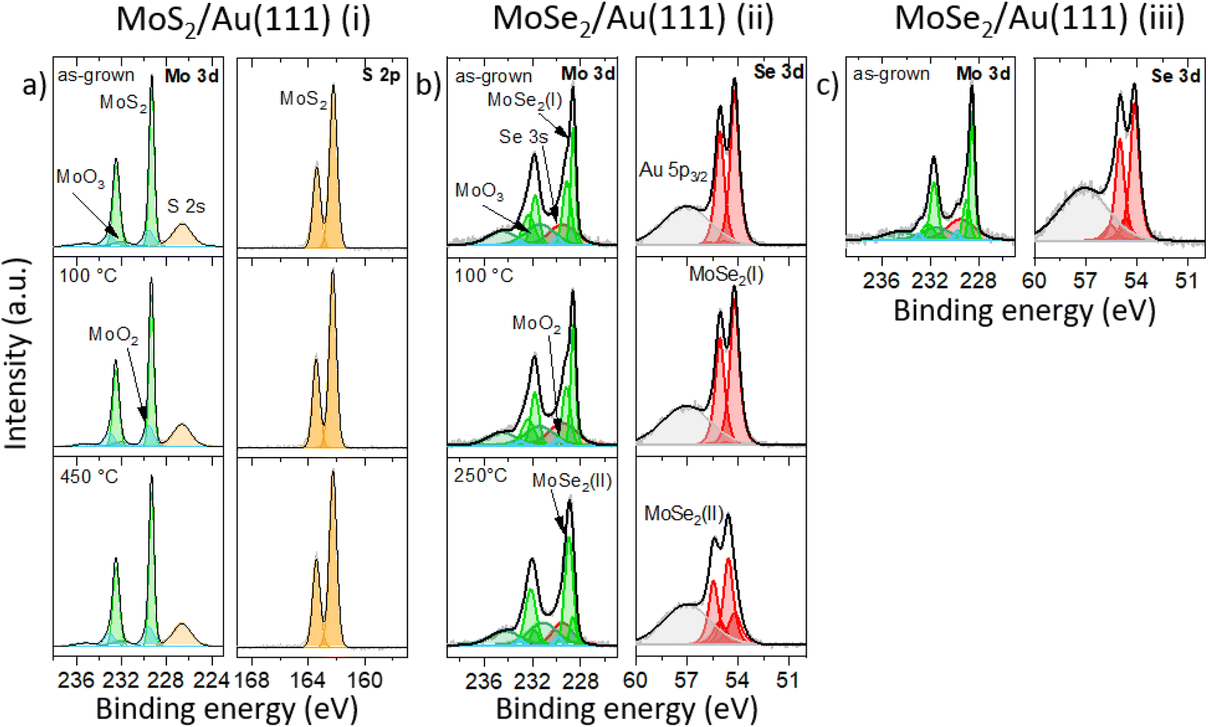 | ||
| Fig. 2 High-resolution XP spectra of (a) MoS2 sample (i), (b) MoSe2 sample (ii) and (c) MoSe2 sample (iii) on Au(111). Mo 3d, S 2s and S 2p spectra of the MoS2 sample (i) as-grown and after different annealing steps in UHV. Mo 3d, Se 3s, Se 3d and Au 5p3/2 spectra of the MoSe2 sample (ii) as-grown and after different annealing steps as well as of the MoSe2 sample (iii) as-grown. In the Mo 3d spectra the peaks related to the TMD monolayers, MoO2, and MoO3 are highlighted in green, light blue or dark green, respectively. | ||
In contrast, the XP spectra for MoSe2 sample (ii) show a distinctively different behavior, Fig. 2b. On the one hand, the Mo 3d and Se 3d spectra are much more complex. On the other hand, we see temperature-dependent changes in the relevant XP signals. For the as-grown and moderately annealed (100 °C) sample (ii), we can identify two doublets (MoSe2 (I), (II)) at BE = 228.6 eV (Mo 3d5/2) and 231.8 eV (Mo 3d3/2) as well as 229.1 eV (Mo 3d5/2) and 232.3 eV (Mo 3d3/2) related to two different MoSe2 monolayer phases. In the following, we name them MoSe2 phase (I) and MoSe2 phase (II), respectively. The most intense component (phase (I)) is localized at lower BEs. Since the intensity of the MoSe2 phase (I) is approximately 33% larger than for phase (II), the second phase is not visible in the Raman spectrum (see red curve in Fig. 1b). Also, in the Se 3d spectra we can distinguish two different doublets at BE = 54.2 eV (Se 3d5/2) and 55.1 eV (Se 3d3/2) as well as at 54.8 eV (Se 3d5/2) and 55.7 eV (Se 3d3/2) corresponding to the two different MoSe2 monolayer phases which are also observed in the Mo 3d region. After annealing of sample (ii) at 250 °C, the intensity of the Mo 3d peaks of phase (II) is now significantly higher (∼5 times) than for phase (I), allowing the second phase with distinct E′ mode to be clearly seen in Raman spectroscopy (see green curve in Fig. 1b). BEs of the characteristic Mo and chalcogen XPS peaks are summarized in Table 1. The Se:Mo ratio is calculated to be (2.0 ± 0.3):1 for the as-grown samples and samples moderately annealed at 100 °C, and (1.9 ± 0.3):1 for the sample annealed at 250 °C (ii). Note that due to the overlapping of the Se 3d peaks with the Au 5p3/2 peak a precise quantification of the Se amount is challenging. From Raman spectroscopy and XPS results we conclude that MoSe2 phase (I) and MoSe2 phase (II) can be assigned to MoSe2 monolayer areas which are weakly or strongly interact with the substrate, respectively.
For the MoSe2 sample (iii) annealed at 100 °C (Fig. 2c), we detect an increased Se:Mo ratio of (2.7 ± 0.3):1 in comparison to the MoSe2 sample (ii) annealed at 100 °C (cf.Fig. 2b). Here, the amount of excess Se can be quantified to approximately 35%. The relevant XP spectra (Fig. 2c) look qualitatively similar to the spectra of the as-grown and 100 °C annealed sample (ii) with less Se (see Fig. 2b). This appearance means that the MoSe2 phase (I) is dominant in comparison to phase (II) which agrees with the Raman spectroscopy data (cf. black and red curve in Fig. 1b). We will refer to these results in the structural and electronic characterization parts again. As we have already described for MoS2, the additional peaks in the Mo 3d spectra arise from MoO2 (light blue) and MoO3 (dark green) precursor residuals.38
2.2 Structural characterization: STM and LEED
Before we start discussing the structural results, we would like to point out that all samples discussed in this section were annealed at 100 °C in UHV (unless otherwise described) to remove contaminations. First, we focus on the structure of MoS2 on Au(111) (sample (i)). In our measurements, the moiré structure22,24,26–29 is observed in the STM image, the fast Fourier transform (FFT) of the STM image, and the LEED pattern (Fig. 3a). This moiré structure arises from the lattice mismatch between Au(111) (2.88 Å) and MoS2 (3.15 Å) with a zero twist angle between the lattices.22,39 In the large area STM images, defects are slightly visible as black dots which originate probably from single sulfur vacancies.40 The close-up STM image in Fig. 3a shows the topmost S layer22 with atomic resolution. Using a quantitative LEED analysis, we determine the lattice parameters of this sample precisely (see Table 2; e.g., lattice constant of 3.15 ± 0.01 Å) by fitting all visible LEED spots and taking multiple scattering up to the 2nd order of the substrate lattice into account. The simulation of the fitted structure is shown in the LEED pattern with yellow circles, Fig. 3b. Also, the moiré structure (light blue unit cell in Fig. 3b) was fitted with inclusion of the same visible spots, whereby the lattice constants were determined to be 33.3 ± 0.3 Å and 33.9 ± 0.3 Å, respectively, which are in agreement with the results from our quantitative FFT analysis of the LT STM image (Table 2) and ref. 24. After annealing at 450 °C, the structure visible in STM (not shown) and the LEED pattern do not change (Fig. S3a and d†). | ||
| Fig. 3 STM and LEED data of (a) MoS2 (i), (b) MoSe2 (ii), and (c) MoSe2 (iii) on Au(111). For MoS2 (i) and MoSe2 (ii), the moiré structures are visible. For MoSe2 (iii), another structure is observed besides the MoSe2 lattice originating from an ordered Se8 interlayer41 discussed in the text. As insets, we show in (a) and (b) atomically resolved STM images of MoS2 and MoSe2 with the moiré contrast being also present and in (c) a close-up image of the MoSe2 structure on this Se interlayer. To increase the visibility of the features, the contrast of the FFT image in (c) was inverted. In the FFT and the LEED patterns the MoS2 (yellow), the moiré structure of MoS2 (light blue), the MoSe2 (green), the moiré structure of MoSe2 (magenta), the Se8 interlayer (blue) structure as well as the Au(111) structure (red) are simulated. Note that sample (i) and (iii) were annealed at 100 °C, sample (ii) was annealed at 250 °C and STM images in (a) are drift-corrected (see Experimental section). STM conditions: (a) 293 K, 0.5 V, 0.5 nA; (a)[inset] 293 K, 0.5 V, 1.5 nA; (b) 4.2 K, 0.4 V, 50 pA; (b)[inset] 4.2 K, 1.5, 20 pA; (c) 4.2 K, 0.1 V, 80 pA. Used LEED equipment: (a) single MCP LEED (ScientaOmicron); (b) and (c) BDL800IR MCP2 (OCI). | ||
 ,
,  ,
,  and
and  are the lengths of lattice vectors, the enclosing angle of these vectors, as well as the angle between the first adsorbate vector
  and the first substrate vector
  , respectively. The moiré lattice parameters are obtained from the same LEED spots as for MoS2 and MoSe2 (Fig. 3). For the Se superstructure analyzed by the FFT of the STM image, two different values for both angles are given. The values given in square brackets have the same convention as in ref. 41, so that
  is smaller than 90°. Note, that the STM (thus also the FFT) images and the LEED patterns of sample (ii) and (iii) were measured at 4.2 K or RT, respectively. This difference can explain the deviations between the values of the Se8 superstructure since slight temperature-dependent structural changes cannot excluded
| Structure |
|
|
|
|
|---|---|---|---|---|
| (i) MoS2/Au(111) (LEED, RT) | 3.15(1) | 3.15(1) | 120.00(4) | 0.00(3) |
| (i) MoS2/Au(111) moiré (LEED, RT) | 33.3(3) | 33.9(3) | 120.1(6) | 0.7(6) |
| (i) MoS2/Au(111) moiré (FFT, RT) | 34(2) | 34(2) | 119.7(9) | 0(1) |
| (ii) MoSe2/Au(111) (LEED, RT) | 3.27(1) | 3.28(1) | 120.00(4) | 0.00(2) |
| (ii) MoSe2/Au(111) moiré (LEED, RT) | 23.0(1) | 23.0(1) | 120.0(1) | 0.0(1) |
| (ii) MoSe2/Au(111) moiré (FFT, 4.2 K) | 22(1) | 22(1) | 120(1) | 5(1) |
| (iii) Se8 superstructure (LEED, RT) | 7.54(1) | 8.64(1) | 116.46(7) | 38.7(2) |
| (iii) Se8 superstructure (FFT, 4.2 K) | 8.41(8) | 8.48(8) | 98.8(6) [81.2(6)] | 43.0(5) [−17.0(5)] |


Next, we characterized the MoSe2 sample (ii) on Au(111) with a lower Se amount according to XPS. Here, we also measured an atomically resolved STM image and a LEED pattern with the typical moiré pattern,23–25 whereby the moiré contrast in the STM image is less pronounced as compared to MoS2 (Fig. 3b). Similar as for the MoS2 sample, in the STM image defects are also slightly visible as black dots. From the quantitative LEED analysis including all visible spots, we estimate the moiré lattice constant to be 23.0 ± 0.1 Å (Table 2). The moiré unit cell is shown in magenta (FFT of STM image and LEED pattern in Fig. 3b). Furthermore, from the same LEED spots, we precisely extract the lattice parameters of MoSe2 (green unit cell) by considering multiple scattering in a similar manner as for the MoS2 sample (i). The lattice parameters are shown in Table 2, matching very well the lattice parameters of freestanding MoSe2.39 Furthermore, after annealing, all LEED spots become more intense (see Fig. S3b and e†), most likely due to desorption of airborne contaminations, which is also reflected in a reduced intensity of the C 1s peak in XPS (not shown). However, the position of the LEED spots does not change, so we do not observe by LEED and STM two different monolayer phases concluded from the XPS data. A possible explanation is that both phases have the same orientation and a similar lattice making them difficult to distinguish in our structural analysis. For a detailed discussion of both phases, we will refer to the analysis in the ARUPS part below (Section 2.3). Since we have not observed any further LEED structure, we suggest that the excess Se, detected by XPS (see Section 1.1), form a disordered layer which vanish after annealing at elevated temperatures.
For the MoSe2 sample with a higher Se concentration (sample (iii)), besides the MoSe2 pattern also another pattern is observed in LEED after a moderate annealing at 100 °C (Fig. 3c), whereas only the moiré structure was faintly visible before annealing (Fig. S3f†). Using STM, it was possible to measure an atomically resolved MoSe2 layer (Fig. 3c). In the corresponding FFT, we can clearly identify a 6-fold symmetric structure confirming the MoSe2 structure (green structure in Fig. 3c). This structure overlaps with another structure which is visible as black dots with a nearly quadratic unit cell in the original STM image. To visualize this structure better, we filtered out the MoSe2 structure from the STM image (Fig. S4†). Moreover, we were able to measure another structure at positions which were not covered with MoSe2 (Fig. S5†). We attribute this structure to the Se8 superstructure reported on Au(111).41 By comparison of the STM images in Fig. S5† and in Fig. 3c, we conclude that the MoSe2 monolayer is on top of a Se8 interlayer. This conclusion is supported by the quantitative FFT analysis of sample (iii) shown in Fig. 3c (blue unit cell). The obtained lattice parameters (Table 2) match the parameters of the Se8 superstructure on Au(111)41 very well. Note that the values of this superstructure were distortion-corrected by using the known MoSe2 structure which is also visible in the FFT (green lattice).
At the end of this section we come back to the LEED pattern in Fig. 3c. Besides the MoSe2 structure (green LEED structure) another structure was observed. We found a model describing almost all other LEED spots by considering multiple scattering, mirror and rotational domains (blue LEED structure). These spots originate from the Se8 superstructure. The lattice parameters fitted to the LEED pattern, shown in Table 2, are different in comparison to the Se8 superstructure observed in the FFT of the STM image. One possible explanation could be that some temperature-dependent structural changes of the Se interlayer occur, since LEED and STM measurements were carried out at RT and 4.2 K, respectively. The unexplained spots might stem from a different Se structure present on the surface.
2.3 Electronic properties: ARUPS and STS
Finally, we focus on the electronic properties of the TMD samples. All data discussed in this chapter were obtained after a moderate annealing step at 100 °C in UHV (unless otherwise described). The ST spectrum of MoS2 on Au(111) (sample (i)) shows a band gap calculated from the onsets of the valence and conduction band of (1.4 ± 0.1) eV (see Fig. S6a†). This value is smaller than the value for a freestanding MoS2 monolayer because of hybridization with the substrate and bandgap renormalization at the Au(111) surface.27,29 Small variations of the onsets of valence and conduction band could be due to defect states in the band gap.12,40 In the ST spectrum of the MoSe2 sample (iii) with a higher Se concentration, we observe a shift of the complete spectrum by 0.5 V compared to the spectrum of sample (ii) which is similar to the reported spectrum in ref. 29. The measured bandgap of sample (ii) (∼1.9 eV) and sample (iii) (∼1.7 eV) are almost the same (Fig. S6b and c†).To study the valence band structure of MoS2 and MoSe2 on Au(111), we carried out ARUPS along the Γ–K direction. First, we discuss the band structure of MoS2 on Au(111), Fig. 4a. Mo 4d and S 3p orbitals generally contribute to the valence band structure. At the Γ point, bands originate from the out-of-plane Mo 4dz and S 3pz orbitals which are responsible for the hybridization with the substrate.42,43 In contrast, the Mo 4dx2−y2 and S 3pxy orbitals contribute to the band structure at the K point leading to spin–orbit splitting.43–45 In our measurement, one MoS2 phase is observed and its valence band maximum (VBM) is localized at the K point, which is typical for the monolayer.39,46 The VBM is localized at a BE = 1.4 eV, matching the valence band offset of the respective ST spectrum in Fig. S6.† In the zoom-in image taken with the 2D detector, we can resolve the spin–orbit split bands with an energetic separation of (120 ± 10) meV (Fig. 4a), which corresponds roughly to the theoretical value of 148 meV.39 In contrast to ARPES measurements of the CVD grown MoS2 monolayers on highly-oriented pyrolytic graphite (HOPG)47 we clearly observe a spin–orbit splitting of the valence band in our measurements. Moreover, the band structure at the Γ point shows a strong spectral broadening due to the hybridization between the MoS2 monolayer and the substrate.29 Since all MoS2 samples with different S to Mo ratio show the same properties according to Raman spectroscopy, LEED and STM we conclude that we do not see an influence of excess S atoms on the electronic structure of MoS2.
 | ||
| Fig. 4 Angle-resolved UP spectra of (a) MoS2 (i) annealed at 100 °C, MoSe2 (ii) annealed at (b) 100 °C and at (c) 250 °C as well as (d) MoSe2 (iii) on Au(111) annealed at 100 °C. In the top parts, the band structures along Γ–K direction are shown. Below, detailed parts of the band structure acquired with the 2D detector around the K points are presented. | ||
For MoSe2 sample (ii), we expect temperature-dependent changes in the ARUPS data, because Raman spectroscopy and XPS suggest a stronger substrate interaction after annealing at 250 °C compared to the annealing at lower temperatures. Generally, Mo 4d and Se 4p orbitals contribute to the valence band structure of MoSe2. In the ARUPS measurement of the MoSe2 sample (ii) on Au(111) directly after the preparation, it was not possible to measure any features of MoSe2 due to contaminations on top of the sample (Fig. S7†). After annealing at 100 °C, the MoSe2 bands become visible, Fig. 4b. The VBM is also localized at the K point, confirming the monolayer formation of MoSe2.39 In the close-up image taken with the 2D detector (Fig. 4b below), we observe two spin–orbit split bands at the K point (four bands in total) with different binding energies and the more intense bands at a lower BE (maxima at BE ≈ 0.6 eV and 0.8 eV). The other spin–orbit split bands are faintly visible at BEs of the maxima of 1.0 and 1.2 eV. Since we also observed two doublets corresponding to MoSe2 monolayers with different intensities in the Mo 3d and Se 3d core level spectra, we correlate these two different XPS doublets with the two phases observed in the valence band structure, which can be assigned to the presence of two monolayer phases differently interacting with the gold substrate. By qualitative comparison of the XPS and ARUPS intensities, the XPS doublet at smaller BEs and the spin–orbit split bands located at smaller BEs in the ARUPS data can be assigned to the MoSe2 phase (I) which weakly interacts with the Au(111) substrate as well as the XPS and ARUPS features at higher BEs correlate with the MoSe2 phase (II) which strongly interacts with the substrate. The spin–orbit splitting at the K point for the more intense bands (phase (I)) at lower binding energies is (180 ± 10) meV (Fig. 4b), which is in good agreement with the theoretically calculated value of 185 meV.39
Next, the MoSe2 sample (ii) was annealed at 250 °C. Based on the Raman spectroscopy and XPS results, we expect a change in the band structure and a stronger MoSe2/substrate-interaction. In agreement with this expectation, the bands at higher binding energies (phase (II)) become more intense (Fig. 4c), and the VBM of this band structure is located at the K point at BE ≈ 1.0 eV (Fig. 4c below). Therewith, we confirm that we have the same two different monolayer phases of MoSe2 on the sample as before, but the intensity ratio between both phases is drastically changed. The band structure of phase (II) (see Fig. 4c) shows a larger broadening of the bands at the Γ point compared to the band structure of phase (I) (see Fig. 4b), resulting from the hybridization with the Au(111) substrate similar as for MoS2 monolayer on Au(111). In addition, the splitting at the K point of phase (II) is reduced in comparison to phase (I) and determined to be (150 ± 10) meV. This change indicates that the valence bands at the K point are also influenced by a coupling effect to the Au(111) substrate. Therefore, we suggest, on the one hand, that the band structure at higher binding energies originates from MoSe2 which is hybridized with the Au(111) substrate. On the other hand, the band structure at lower binding energies is caused by decoupled MoSe2 probably due to disordered Se atoms in between MoSe2 and substrate. Both conclusions are supported by our Raman spectroscopy results discussed above. The decoupling of the MoSe2 is achieved by residual Se atoms underneath the TMD layer. Two MoSe2 monolayer phases are observable in XPS and ARUPS for both annealing steps at 100 °C and 250 °C. At higher annealing temperature we can remove additional Se atoms to a large extent, and phase (II) becomes dominant whereas the weakly interacting phase (I) is dominant at annealing temperatures smaller than 100 °C.
Finally, we discuss the ARUPS data of MoSe2 sample (iii) with the Se superstructure between MoSe2 and Au(111). The measured band structure in Fig. 4d shows a similar behavior as for the MoSe2 sample (ii) annealed at 100 °C (cf.Fig. 4b). This result means that the MoSe2 phase (I) with the VBM at ≈0.6 eV is dominant and the splitting at the K point is (170 ± 10) meV, whereby the electronic structure is hardly or not influenced by the Se8 superstructure. These ARUPS findings agree with the results from Raman spectroscopy and XPS and are summarized in Table 1. Finally, our experimental data suggest that the decoupling effect of the MoSe2 monolayer is caused either by a periodic Se interlayer or by some disordered intercalated Se atoms. In contrast, for MoS2 monolayers we do not observe intercalation of the excess S atoms. This difference in comparison to the MoSe2 monolayers may result from a stronger chemical binding of selenium to Au(111).48,49 Most probably, a weaker interaction of sulfur to Au(111) is insufficient to achieve the intercalation. Note that the interatomic distance of the MoSe2 monolayer to Au(111) is higher than that of the MoS2,50 which can also facilitate intercalation of the chalcogen atoms.
3 Conclusion
In summary, we investigated MoS2 and MoSe2 monolayers epitaxially grown on an Au(111) single crystal by CVD at ambient pressure. These two-dimensional films were characterized by complementary surface sensitive methods. Raman spectroscopy, scanning tunneling microscopy, X-ray and angle-resolved ultraviolet photoelectron spectroscopy confirm the formation of high-quality monolayers of both TMDs on the Au(111) surface. For MoS2, the moiré structure, Raman modes, as well as the band structure demonstrate strong interaction of the monolayer with the substrate. Even after annealing at 450 °C no significant changes in comparison to the non-annealed samples were observed. In contrast, MoSe2 monolayers show a different behavior. For as-grown and moderately annealed samples (<100 °C) we observed a weak interaction of MoSe2 with the Au(111) substrate due to the formation of a periodic as well as disordered Se interlayer. After annealing at 250 °C, due to desorption of this excess intercalated Se, we found that the interaction of the MoSe2 monolayer with the gold substrate increases, which is reflected in both Raman spectroscopy and photoelectron spectroscopy data. Our study is a step towards the rational design of TMD monolayer/Au interfaces which are important for the engineering of efficient electrical contacts for a variety of electronic and optoelectronic devices based on TMD monolayers.4 Experimental section
4.1 Sample preparation
Before the growth process, the Au(111) single crystal (MaTecK, Jülich, Germany) with a purity of 99.999% was cleaned by several cycles of Ar+-sputtering (1 kV, 30 min, ≈4 μA cm−2) and annealing (≈600 °C, 30 min) in an ultrahigh vacuum (UHV) chamber. For the growth, we used a CVD process in a two-zone furnace outside of the UHV system at ambient pressure, as described in ref. 7. In the first zone, the S powder (purity of 99.98%, Sigma Aldrich) or the Se pellets (purity of 99.98%, Sigma Aldrich) were placed in a Knudsen cell and heated up to 200 °C (sample (i)) or 300 °C (sample (ii)), respectively. Additionally, for the MoSe2 sample with a higher amount of Se discussed in the paper, we heated the Knudsen cell with the Se pellets up to 450 °C (sample (iii)) to provide this excess Se concentration. The MoO3 precursor (purity of 99.97%, Sigma Aldrich) and the prepared Au(111) single crystal were placed into the second zone. Here, the temperature was held at 700 °C and 750 °C to prepare MoS2 and MoSe2, respectively. In addition, a mixture of Ar and H2 (100 sccm and 10 sccm, respectively) was used as carrier gas. The subsequent annealing steps of the TMD samples were carried out in a UHV chamber to clean the sample from airborne impurities.4.2 Optical microscopy
Optical microscopy was performed using a Zeiss Axio Imager Z1.m microscope in brightfield mode. The microscope includes a thermoelectrically cooled 5 MP CCD camera.4.3 Raman spectroscopy
The Raman spectra were measured using a Bruker Senterra spectrometer operated in backscattering mode at ambient conditions. The utilized wavelength of 532 nm was obtained from a frequency-doubled Nd:YAG laser. A 50× objective and a thermoelectrically cooled CCD detector (−65 °C) were used. The spectral resolution of the system is 2–3 cm−1.4.4 Scanning tunneling microscopy/spectroscopy
The following techniques were carried out in UHV at a base pressure < 3 × 10⁻¹⁰ mbar. For scanning tunneling microscopy (STM) and spectroscopy (STS), we used two different systems. On the one hand, we measured with a VT SPM (Scienta Omicron) at room temperature (RT) using a W tip. On the other hand, STM images were also acquired using a SPECS JT-STM/AFM at 4.2 K with a Pt/Ir tip. All images were evaluated with Gwyddion (Version 2.56).51 The RT STM images were drift corrected using the autocorrelation function and calibrated by the lattice parameters obtained from LEED analysis. For quantitative analysis of the fast Fourier transform (FFT) of the STM images, the LEEDLab software was used.52 ST spectra were obtained by means of a lock-in amplifier at RT or liquid helium temperatures. A description of the estimation of the band gap values is given in Fig. S6.†4.5 Distortion-corrected low-energy electron diffraction
Low-energy electron diffraction (LEED) images of the TMD layers were acquired using dual microchannel plates (MCP2-SpectaLEED, Omicron; BDL800IR MCP2, OCI Vacuum Microengineering) or a single microchannel plate (SMCP, Scienta Omicron) LEED-system. All pictures were corrected for geometrical distortions and the energy error using the LEEDCal software.53,54 After that, the obtained images were analyzed with the LEEDLab software to quantify the reciprocal structures of the visible LEED spots with an accuracy of typically 1%.52 For the Au(111) surface a lattice constant of 2.884 Å was used.554.6 X-ray and (angle-resolved) ultraviolet photoelectron spectroscopy
X-ray photoelectron spectroscopy (XPS) was performed at two different systems using monochromatized Al Kα radiation (SPECS Focus 500 and Scienta Omicron XM1200) and electron analyzers with a spectral energy resolution of 0.5 eV and 0.6 eV (SPECS PHOIBOS 150 and Argus CU), respectively. The spectra were calibrated to the Au 4f7/2 peak (84.0 eV) and fitted by Voigt functions (Gaussian:Lorentzian = 70:30) after subtraction of a linear (S 2p, Se 3d) or Shirley (Mo 3d) background. Ultraviolet photoelectron spectroscopy (UPS) was carried out with monochromatized and p-polarized He Iα excitation (SPECS ultraviolet light source (UVLS)). Band structures were measured by tilting the sample and therefore changing the photoemission angle (angle-resolved UPS (ARUPS)). The binding energy of the UP spectra was calibrated to the Fermi edge of Au(111), whereby an energy resolution of 60 meV were used. For detailed band structure measurements, we used the 2D mode of the detector. All photoelectron spectroscopy measurements were carried out at room temperature.
Author contributions
The manuscript was written with contributions of all authors.Conflicts of interest
There are no conflicts to declare.Acknowledgements
This research was supported by the Deutsche Forschungsgemeinschaft (DFG) through a research infrastructure grant INST 275/257-1 FUGG (313713174), CRC 1375 NOA (Project B2, 398816777), SPP2244 (Project TU149/13-1, 443361515) and DFG individual grant TU149/16-1 (464283495). We acknowledge support by the German Research Foundation Projekt-No. 512648189 and the Open Access Publication Fund of the Thueringer Universitaets - und Landesbibliothek Jena. The authors thank Stephanie Höppener and Ulrich S. Schubert for enabling Raman spectroscopy studies at the Jena Center for Soft Matter (JCSM) as well as Shahab Mohebi Fard and Emad Najafidehaghani for discussions and the artist views on the samples studied in this work.References
- P. Eickholt, C. Sanders, M. Dendzik, L. Bignardi, D. Lizzit, S. Lizzit, A. Bruix, P. Hofmann and M. Donath, Spin Structure of K Valleys in Single-Layer WS2 on Au(111), Phys. Rev. Lett., 2018, 121, 136402 CrossRef CAS PubMed.
- J. Sun, H. Hu, D. Pan, S. Zhang and H. Xu, Selectively Depopulating Valley-Polarized Excitons in Monolayer MoS2 by Local Chirality in Single Plasmonic Nanocavity, Nano Lett., 2020, 20, 4953–4959 CrossRef CAS PubMed.
- M. D. Tran, J.-H. Kim and Y. H. Lee, Tailoring photoluminescence of monolayer transition metal dichalcogenides, Curr. Appl. Phys., 2016, 16, 1159–1174 CrossRef.
- L. Sun, X. Zhang, F. Liu, Y. Shen, X. Fan, S. Zheng, J. T. Thong, Z. Liu, S. A. Yang and H. Y. Yang, Vacuum level dependent photoluminescence in chemical vapor deposition-grown monolayer MoS2, Sci. Rep., 2017, 7, 1–9 CrossRef.
- C.-H. Lee, G.-H. Lee, A. M. Van Der Zande, W. Chen, Y. Li, M. Han, X. Cui, G. Arefe, C. Nuckolls and T. F. Heinz, Atomically thin p–n junctions with van der Waals heterointerfaces, Nat. Nanotechnol., 2014, 9, 676–681 CrossRef CAS PubMed.
- X.-R. Wang, Y. Shi and R. Zhang, Field-effect transistors based on two-dimensional materials for logic applications, Chin. Phys. B, 2013, 22, 098505 CrossRef.
- A. George, C. Neumann, D. Kaiser, R. Mupparapu, T. Lehnert, U. Hübner, Z. Tang, A. Winter, U. Kaiser and I. Staude, Controlled growth of transition metal dichalcogenide monolayers using Knudsen-type effusion cells for the precursors, J. Phys.: Mater., 2019, 2, 016001 CAS.
- S. Najmaei, X. Zou, D. Er, J. Li, Z. Jin, W. Gao, Q. Zhang, S. Park, L. Ge, S. Lei, J. Kono, V. B. Shenoy, B. I. Yakobson, A. George, P. M. Ajayan and J. Lou, Tailoring the Physical Properties of Molybdenum Disulfide Monolayers by Control of Interfacial Chemistry, Nano Lett., 2014, 14, 1354–1361 CrossRef CAS PubMed.
- E. Najafidehaghani, Z. Gan, A. George, T. Lehnert, G. Q. Ngo, C. Neumann, T. Bucher, I. Staude, D. Kaiser and T. Vogl, 1D p–n Junction Electronic and Optoelectronic Devices from Transition Metal Dichalcogenide Lateral Heterostructures Grown by One-Pot Chemical Vapor Deposition Synthesis, Adv. Funct. Mater., 2021, 31, 2101086 CrossRef CAS.
- Z. Gan, E. Najafidehaghani, S. H. Han, S. Shradha, F. Abtahi, C. Neumann, J. Picker, T. Vogl, U. Hübner and F. Eilenberger, Patterned Growth of Transition Metal Dichalcogenide Monolayers and Multilayers for Electronic and Optoelectronic Device Applications, Small Methods, 2022, 6, 2200300 CrossRef CAS PubMed.
- K. F. Mak and J. Shan, Photonics and optoelectronics of 2D semiconductor transition metal dichalcogenides, Nat. Photonics, 2016, 10, 216–226 CrossRef CAS.
- A. George, M. V. Fistul, M. Gruenewald, D. Kaiser, T. Lehnert, R. Mupparapu, C. Neumann, U. Hübner, M. Schaal, N. Masurkar, L. M. R. Arava, I. Staude, U. Kaiser, T. Fritz and A. Turchanin, Giant persistent photoconductivity in monolayer MoS2 field-effect transistors, npj 2D Mater. Appl., 2021, 5, 15 CrossRef CAS.
- S. Klimmer, O. Ghaebi, Z. Gan, A. George, A. Turchanin, G. Cerullo and G. Soavi, All-optical polarization and amplitude modulation of second-harmonic generation in atomically thin semiconductors, Nat. Photonics, 2021, 15, 837–842 CrossRef CAS.
- G. Q. Ngo, E. Najafidehaghani, Z. Gan, S. Khazaee, M. P. Siems, A. George, E. P. Schartner, S. Nolte, H. Ebendorff-Heidepriem, T. Pertsch, A. Tuniz, M. A. Schmidt, U. Peschel, A. Turchanin and F. Eilenberger, In-fibre second-harmonic generation with embedded two-dimensional materials, Nat. Photonics, 2022, 16, 769–776 CrossRef CAS.
- S. Lei, F. Wen, B. Li, Q. Wang, Y. Huang, Y. Gong, Y. He, P. Dong, J. Bellah, A. George, L. Ge, J. Lou, N. J. Halas, R. Vajtai and P. M. Ajayan, Optoelectronic Memory Using Two-Dimensional Materials, Nano Lett., 2015, 15, 259–265 CrossRef CAS PubMed.
- T. Pham, G. Li, E. Bekyarova, M. E. Itkis and A. Mulchandani, MoS2-Based Optoelectronic Gas Sensor with Sub-parts-per-billion Limit of NO2 Gas Detection, ACS Nano, 2019, 13, 3196–3205 CrossRef CAS PubMed.
- B. Liu, L. Chen, G. Liu, A. N. Abbas, M. Fathi and C. Zhou, High-Performance Chemical Sensing Using Schottky-Contacted Chemical Vapor Deposition Grown Monolayer MoS2 Transistors, ACS Nano, 2014, 8, 5304–5314 CrossRef CAS PubMed.
- S. Shree, A. George, T. Lehnert, C. Neumann, M. Benelajla, C. Robert, X. Marie, K. Watanabe, T. Taniguchi and U. Kaiser, High optical quality of MoS2 monolayers grown by chemical vapor deposition, 2D Mater., 2019, 7, 015011 CrossRef.
- A. Barton, R. Yue, S. Anwar, H. Zhu, X. Peng, S. McDonnell, N. Lu, R. Addou, L. Colombo and M. Kim, Transition metal dichalcogenide and hexagonal boron nitride heterostructures grown by molecular beam epitaxy, Microelectron. Eng., 2015, 147, 306–309 CrossRef CAS.
- H. Li, J. Wu, Z. Yin and H. Zhang, Preparation and Applications of Mechanically Exfoliated Single-Layer and Multilayer MoS2 and WSe2 Nanosheets, Acc. Chem. Res., 2014, 47, 1067–1075 CrossRef CAS PubMed.
- X. Song, Z. Guo, Q. Zhang, P. Zhou, W. Bao and D. W. Zhang, Progress of Large-Scale Synthesis and Electronic Device Application of Two-Dimensional Transition Metal Dichalcogenides, Small, 2017, 13, 1700098 CrossRef.
- S. S. Grønborg, S. Ulstrup, M. Bianchi, M. Dendzik, C. E. Sanders, J. V. Lauritsen, P. Hofmann and J. A. Miwa, Synthesis of epitaxial single-layer MoS2 on Au (111), Langmuir, 2015, 31, 9700–9706 CrossRef.
- F. Cheng, Z. Hu, H. Xu, Y. Shao, J. Su, Z. Chen, W. Ji and K. P. Loh, Interface Engineering of Au(111) for the Growth of 1T′-MoSe2, ACS Nano, 2019, 13, 2316–2323 CAS.
- S. Yasuda, R. Takahashi, R. Osaka, R. Kumagai, Y. Miyata, S. Okada, Y. Hayamizu and K. Murakoshi, Out-of-Plane Strain Induced in a Moiré Superstructure of Monolayer MoS2 and MoSe2 on Au(111), Small, 2017, 13, 1700748 CrossRef.
- J. Lu, D.-L. Bao, K. Qian, S. Zhang, H. Chen, X. Lin, S.-X. Du and H.-J. Gao, Identifying and visualizing the edge terminations of single-layer MoSe2 island epitaxially grown on Au (111), ACS Nano, 2017, 11, 1689–1695 CrossRef CAS PubMed.
- P. Yang, S. Zhang, S. Pan, B. Tang, Y. Liang, X. Zhao, Z. Zhang, J. Shi, Y. Huan and Y. Shi, Epitaxial growth of centimeter-scale single-crystal MoS2 monolayer on Au (111), ACS Nano, 2020, 14, 5036–5045 CrossRef CAS.
- N. Krane, C. Lotze and K. J. Franke, Moiré structure of MoS2 on Au (111): Local structural and electronic properties, Surf. Sci., 2018, 678, 136–142 CrossRef CAS.
- F. Tumino, C. S. Casari, M. Passoni, V. Russo and A. L. Bassi, Pulsed laser deposition of single-layer MoS2 on Au (111): from nanosized crystals to large-area films, Nanoscale Adv., 2019, 1, 643–655 RSC.
- A. Bruix, J. A. Miwa, N. Hauptmann, D. Wegner, S. Ulstrup, S. S. Grønborg, C. E. Sanders, M. Dendzik, A. Grubišić Čabo, M. Bianchi, J. V. Lauritsen, A. A. Khajetoorians, B. Hammer and P. Hofmann, Single-layer MoS2 on Au(111): Band gap renormalization and substrate interaction, Phys. Rev. B, 2016, 93, 165422 CrossRef.
- A. Grubišić Čabo, J. A. Miwa, S. S. Grønborg, J. M. Riley, J. C. Johannsen, C. Cacho, O. Alexander, R. T. Chapman, E. Springate, M. Grioni, J. V. Lauritsen, P. D. C. King, P. Hofmann and S. Ulstrup, Observation of Ultrafast Free Carrier Dynamics in Single Layer MoS2, Nano Lett., 2015, 15, 5883–5887 CrossRef PubMed.
- C. C. Silva, D. Dombrowski, N. Atodiresei, W. Jolie, F. F. zum Hagen, J. Cai, P. T. Ryan, P. K. Thakur, V. Caciuc and S. Blügel, Spatial variation of geometry, binding, and electronic properties in the moiré superstructure of MoS2 on Au (111), 2D Mater., 2022, 9, 025003 CrossRef.
- L. Bignardi, D. Lizzit, H. Bana, E. Travaglia, P. Lacovig, C. E. Sanders, M. Dendzik, M. Michiardi, M. Bianchi, M. Ewert, L. Buß, J. Falta, J. I. Flege, A. Baraldi, R. Larciprete, P. Hofmann and S. Lizzit, Growth and structure of singly oriented single-layer tungsten disulfide on Au(111), Phys. Rev. Mater., 2019, 3, 014003 CrossRef CAS.
- H. Bana, E. Travaglia, L. Bignardi, P. Lacovig, C. E. Sanders, M. Dendzik, M. Michiardi, M. Bianchi, D. Lizzit and F. Presel, Epitaxial growth of single-orientation high-quality MoS2 monolayers, 2D Mater., 2018, 5, 035012 CrossRef.
- Q. Wu, M. Bagheri Tagani, L. Zhang, J. Wang, Y. Xia, L. Zhang, S.-Y. Xie, Y. Tian, L.-J. Yin, W. Zhang, A. N. Rudenko, A. T. S. Wee, P. K. J. Wong and Z. Qin, Electronic Tuning in WSe2/Au via van der Waals Interface Twisting and Intercalation, ACS Nano, 2022, 16, 6541–6551 CrossRef CAS.
- D. S. Schulman, A. J. Arnold and S. Das, Contact engineering for 2D materials and devices, Chem. Soc. Rev., 2018, 47, 3037–3058 RSC.
- F. Tumino, P. D'Agosta, V. Russo, A. Li Bassi and C. S. Casari, Raman Spectroscopy of 2D MoS2 Interacting with Metals, Crystals, 2023, 13, 1271 CrossRef CAS.
- A. Rodriguez, M. Velický, J. Řáhová, V. Zólyomi, J. Koltai, M. Kalbáč and O. Frank, Activation of Raman modes in monolayer transition metal dichalcogenides through strong interaction with gold, Phys. Rev. B, 2022, 105, 195413 CrossRef CAS.
- A. V. Naumkin, A. Kraut-Vass, S. W. Gaarenstroom and C. J. Powell, NIST Standard Reference Database 20, Version 4.1, 2012 Search PubMed.
- Z. Y. Zhu, Y. C. Cheng and U. Schwingenschlögl, Giant spin-orbit-induced spin splitting in two-dimensional transition-metal dichalcogenide semiconductors, Phys. Rev. B: Condens. Matter Mater. Phys., 2011, 84, 153402 CrossRef.
- F. Tumino, C. S. Casari, A. Li Bassi and S. Tosoni, Nature of Point Defects in Single-Layer MoS2 Supported on Au(111), J. Phys. Chem. C, 2020, 124, 12424–12431 CrossRef CAS.
- B. Liu, Y. Zhuang, Y. Que, C. Xu and X. Xiao, STM study of selenium adsorption on Au (111) surface, Chin. Phys. B, 2020, 29, 056801 CrossRef CAS.
- J. D. Fuhr, J. O. Sofo and A. Saúl, Adsorption of Pd on MoS2(1000): Ab initio electronic-structure calculations, Phys. Rev. B: Condens. Matter Mater. Phys., 1999, 60, 8343–8347 CrossRef CAS.
- S. Mahatha, K. Patel and K. S. Menon, Electronic structure investigation of MoS2 and MoSe2 using angle-resolved photoemission spectroscopy and ab initio band structure studies, J. Phys.: Condens. Matter, 2012, 24, 475504 CrossRef CAS PubMed.
- L. F. Mattheiss, Energy Bands for 2H-NbSe2 and 2H-MoS2, Phys. Rev. Lett., 1973, 30, 784–787 CrossRef CAS.
- L. F. Mattheiss, Band Structures of Transition-Metal-Dichalcogenide Layer Compounds, Phys. Rev. B: Solid State, 1973, 8, 3719–3740 CrossRef CAS.
- T. Brumme, M. Calandra and F. Mauri, First-principles theory of field-effect doping in transition-metal dichalcogenides: structural properties, electronic structure, Hall coefficient, and electrical conductivity, Phys. Rev. B: Condens. Matter Mater. Phys., 2015, 91, 155436 CrossRef.
- N. Alidoust, G. Bian, S.-Y. Xu, R. Sankar, M. Neupane, C. Liu, I. Belopolski, D.-X. Qu, J. D. Denlinger and F.-C. Chou, Observation of monolayer valence band spin-orbit effect and induced quantum well states in MoX2, Nat. Commun., 2014, 5, 4673 CrossRef CAS PubMed.
- S. Mankefors, A. Grigoriev and G. Wendin, Molecular alligator clips: a theoretical study of adsorption of S, Se and S–H on Au(111), Nanotechnology, 2003, 14, 849 CrossRef CAS.
- D.-J. Liu, J. W. Evans, P. M. Spurgeon and P. A. Thiel, Structure of chalcogen overlayers on Au(111): Density functional theory and lattice-gas modeling, J. Chem. Phys., 2020, 152, 224706 CrossRef CAS PubMed.
- S. Sarkar and P. Kratzer, Signatures of the Dichalcogenide–Gold Interaction in the Vibrational Spectra of MoS2 and MoSe2 on Au(111), J. Phys. Chem. C, 2021, 125, 26645–26651 CrossRef CAS.
- D. Nečas and P. Klapetek, Gwyddion: an open-source software for SPM data analysis, Open Phys., 2012, 10, 181–188 Search PubMed.
- F. Sojka and T. Fritz, LEEDLab 2018, version 1.0, Fritz & Sojka GbR, Apolda Germany, 2018 Search PubMed.
- F. Sojka, M. Meissner, C. Zwick, R. Forker and T. Fritz, Determination and correction of distortions and systematic errors in low-energy electron diffraction, Rev. Sci. Instrum., 2013, 84, 015111 CrossRef PubMed.
- F. Sojka and T. Fritz, LEEDCal 2013, version 4.0, Fritz & Sojka GbR, Apolda Germany, 2018 Search PubMed.
- B. Dutta and B. Dayal, Lattice Constants and Thermal Expansion of Gold up to 878 °C by X-Ray Method, Phys. Status Solidi B, 1963, 3, 473–477 CrossRef CAS.
Footnote |
| † Electronic supplementary information (ESI) available. See DOI: https://doi.org/10.1039/d3na00475a |
| This journal is © The Royal Society of Chemistry 2024 |