
 Open Access Article
 This Open Access Article is licensed under a Creative Commons Attribution-Non Commercial 3.0 Unported Licence
Graphene-based chemiresistive gas sensors
Patrick
Recum
 and
Thomas
Hirsch
*
and
Thomas
Hirsch
*
University of Regensburg, Germany. E-mail: Patrick.Recum@ur.de; Thomas.Hirsch@ur.de
First published on 23rd October 2023
Abstract
Gas sensors allow the monitoring of the chemical environment of humans, which is often crucial for their wellbeing or even survival. Miniaturization, reversibility, and selectivity are some of the key challenges for serial use of chemical sensors. This tutorial review describes critical aspects when using nanomaterials as sensing substrates for the application in chemiresistive gas sensors. Graphene has been shown to be a promising candidate, as it allows gas sensors to be operated at room temperature, possibly saving large amounts of energy. In this review, an overview is given on the general mechanisms for gas-sensitive semiconducting materials and the implications of doping and functionalization on the sensing parameters of chemiresistive devices. It shows in detail how different challenges, like sensitivity, response time, reversibility and selectivity have been approached by material development and operation modes. In addition, perspectives from the area of data analysis and intelligent algorithms are presented, which can further enhance these sensors' usability in the field.
 Patrick Recum | Patrick Recum received his Master's degree in chemistry from the University of Regensburg, Germany, where he is currently finishing his PhD studies under the guidance of Thomas Hirsch. His research at the Institute for Analytical Chemistry, Chemo- and Biosensors is focused on tailoring the material properties of reduced graphene oxide for chemical sensing applications. |
 Thomas Hirsch | Thomas Hirsch obtained his PhD in analytical chemistry under the supervision of Prof. Otto Wolfbeis at the University of Regensburg. He is an associate professor at the Institute of Analytical Chemistry, Chemo- and Biosensors of the University of Regensburg. His research deals with the development and characterization of nanomaterials for (bio)analytical applications. |
Introduction
Society is becoming more aware of environmental pollution concerns and the impact of air quality on public health is getting increased attention.1–5 Gases, mostly color- and odorless, have long been overseen for causing health risks after long-term exposure. As an example, only recently it was found that slightly increased levels of O3 or SO2 can lead to cardiovascular diseases.6–8 Other health impacts are caused by NO2, which reduces the lung function or impact organs like the spleen or liver.9Accordingly, guidelines were implemented to minimize the exposure to toxic, or otherwise harmful gases. To reduce health risks by long-term exposure and environmental damages, assessment thresholds have been defined by the European Parliament. These limit concentrations of toxic gases in air over a certain time. Specifically, 166 ppb per day and 33 ppb per year have been set for NO2, 290 ppb per hour and 105 ppb per day for SO2, and 8 ppb in a workday (8 h) for CO.10 Similarly, maximum workplace concentrations, as provided by the German Research Foundation, limit the concentrations for short-term exposure, to 790 ppb for NO2, 2.2 ppm for SO2, 5.9 ppm for H2S, 29 ppm for CO, and 7500 ppm for CO2, respectively.11 However, ensuring the compliance of such limits requires individual monitoring. This and the goal of improving the overall quality of life through the possibility of individual risk evaluation leads to a steadily growing demand for miniaturized gas sensors with low power consumption, that can be implemented in smartphones, smart-watches and smart-homes.12,13 Fields of application additional to safety aspects, such as warning of acute toxic gases and gas leaks, are the control of industrial processes and production, quality control in food, guarantee of functionality as in the lambda probe, monitoring greenhouse gases, and detection of biomarkers in breath.14
Field-effect transistors (FET) and chemiresistive gas sensors can help to overcome the limitations of current analytical methods in achieving an improved local precision of air quality monitoring. In principle, a chemiresistor consists of a sensing material deposited on an inert substrate, modified with a source electrode and a drain electrode or with interdigital electrodes (IDEs). It can be turned into a FET-based sensor by contacting a gate electrode to the semiconducting channel in between to apply a gate voltage.15 Their small form factor together with simplicity, easy fabrication, and high sensitivity at low power consumption makes them well-suited candidates for the integration in a dense information network consisting of several hundreds or thousands of individual sensor stations to monitor toxic and greenhouse gases.16
As the sensitive layer, graphene and its derivatives have been intensively researched over the past decades. Their inherent material properties promise to further enhance the described advantages of chemiresistors and chem-FETs in terms of miniaturization, power consumption, and the abundant resource availability.
New powerful algorithms are being developed to handle the large volumes of geologically widely distributed data expected with the increasing popularity of internet of things (IoT) applications, that require a high number of such sensors.17
Chemiresistive gas sensing mechanisms
Chemiresistive gas sensors respond to changes in resistance caused by electrons that are exchanged when gas molecules interact with either the semiconducting sensing layer or the metal electrodes. These interactions strongly depend on the kind of material, type of gas (reducing or oxidizing), on temperature, pressure, and relative humidity (RH).18–20When a semiconducting sensing layer is contacted by a metal electrode, the Fermi levels (EF) of both materials must line up while in equilibrium. The Fermi level describes the thermodynamic work, which is required to add one electron to a solid-state body, not accounting for the work required to remove the electron from wherever it may come from. For a semiconductor it usually lies within the bandgap. The minimal work required to remove an electron from a point within a solid-state body is called the work function Φ and is equal to the energy difference between the Fermi level and the vacuum level.21 If now the work function of the metal electrode is larger than the work function of the semiconductor (ΦM > ΦSC), high energy electrons from the conduction band (EC) of the semiconductor move from its bulk to the surface of the metal, thereby leaving an electron depletion layer (EDL) at the interface. For n-type materials, where EF lies close to EC and electrons are the majority charge carriers, the emerging, depleted junction is called a Schottky barrier. This type of contact shows rectifying behavior and can be used as a diode. If ΦSC > ΦM, a Schottky barrier is also formed for p-type materials, with EF close to the valence band (EV) and electron–holes (h+) as majority charge carriers. Here, electrons move from the metal surface to the empty states in the valence band of the semiconductor bulk and an electron-accumulation layer/hole-depletion layer (HDL) emerges. In other cases, ohmic contacts are formed. However, these appear to be less relevant for use in chemiresistive gas sensors. The height of the Schottky barrier from metal to semiconductor is mainly governed by ΦM and the electron affinity of the semiconductor. The height and thickness of the built-in potential barrier (Vbuilt-in) across each depletion layer depends on the difference in the work functions.
The effect of chemical-doping on pristine graphene by gaseous molecules was first described by Schedin et al. in 2007.22 Adsorbed oxidizing gas molecules such as NO2, SO2, or water vapor withdraw electrons from the semiconductor, while reducing gases like NH3, H2, and H2S donate electrons to it.23 For n-type semiconductors a decrease in electron density means fewer majority charge carriers and therefore a higher resistance across the sensing layer, while an increasing number of charge carriers leads to a lower resistance. On the other hand, a reduced number of electrons (more h+) results in a lower resistance for a p-type material, while an increasing number of electrons (fewer h+) increases resistance.
Additionally, the chemical doping of the semiconductor by gas molecules is reported to influence the resistance across the Schottky barriers at the electrode contacts.18 Adsorbed electron-donating gases lead to n-doping of the material, such that the semiconductor's Fermi level is shifted towards its conduction band. For n-type materials in contact with an electrode this results in an increase of Vbuilt-in and due to the higher dopant concentration, a reduced thickness of the depletion layer. Consequently, the tunneling probability for electrons increases and the resistance at the junction decreases. The reverse case can be observed for p-doping by electron-withdrawing gases.24 The Fermi levels are shifted in the same way for a p-type material, but with electron holes as the relevant charge carriers the contact resistance is increased by n-doping (reducing gas) and decreased by p-doping (oxidizing gas). In Fig. 1 the effects of such interactions are shown for a Schottky barrier between gold and n-type MoO2 as well p-type reduced graphene oxide (rGO) as examples.
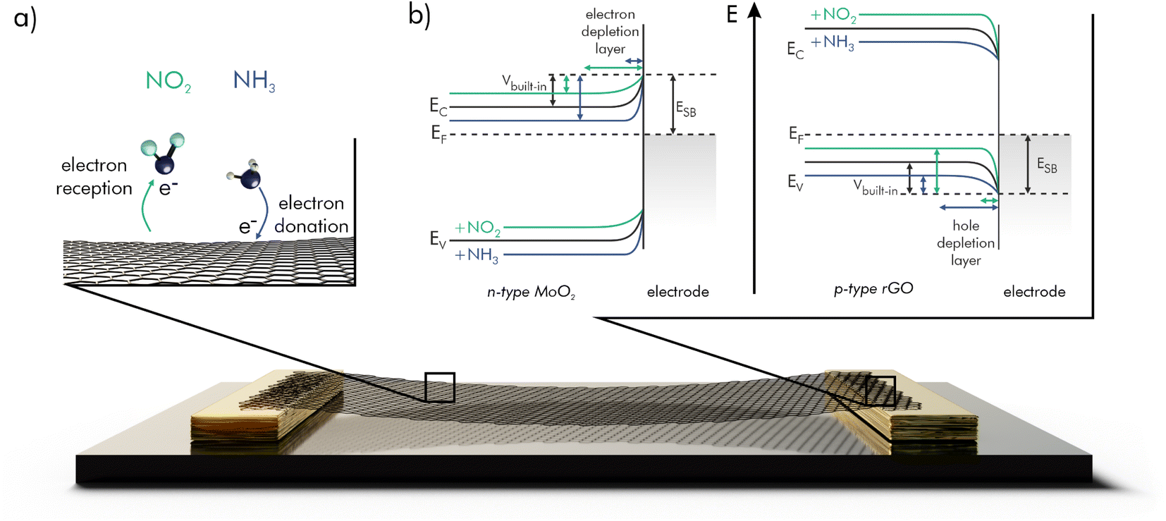 | ||
| Fig. 1 Gas sensing mechanisms on a semiconducting material, such as a graphene derivative; (a) electron exchange between gas molecules and receptor; (b) shift of the band structure at the semiconductor-electrode contact. | ||
Pristine graphene does not form a Schottky barrier with metals due to its semimetallic rather than semiconducting characteristics. However, Schottky junctions can be formed between pristine graphene and various semiconductors.25,26
As a side-effect, the adsorption or desorption of electrons on the metal contact has an influence on the resistance of the sensor.27–29 Specifically, an increase of the metal's work function can be observed, when an oxidizing gas adsorbs, forming surface dipoles. Thereby the Schottky barrier height (ESB) as well as the Vbuilt-in are increased for contacts with n-type and decreased for p-type materials. Again, reducing gases have the exact opposite effect. This is particularly visible for palladium exposed to H2.30 It was found that the choice of electrode metal can have a significant influence on the sensing characteristics.31,32
For each semiconductor–metal pair the respective work-functions Φ, as well as the semiconductor's bandgap (EG) and electron affinity are needed, to determine the type of junction and its behavior. The bandgap of a solution processed material like rGO is often determined by processing the data from its absorption spectrum via a so-called Tauc plot, but the accuracy of the obtained values stands and falls with the quality of the measurement and precise fitting, which is often challenging, especially for solids dispersed in a solvent. A less biased method for the task presents reflection electron energy loss spectroscopy (REELS). Here, an electron beam is reflected from the sample-surface and the loss in energy of the reflected electrons is measured. Because of the broad electron beam (∼1 mm in diameter) a large and homogeneous sample area is necessary.33,34 However, the electron affinity cannot be measured directly, but a workaround can be achieved by finding the highest energy state of the valence band by photoelectron spectroscopy (PES) and subtracting the energy of the bandgap. The entire band-structure of a material can be determined by angle-resolved photoelectron spectroscopy (ARPES),35–37 while the work function of graphene and other materials is usually measured using a Kelvin probe.38
In a typical sensor-architecture the sensitive layer is contacted by two electrodes, often IDEs. A Schottky barrier is formed on each of the semiconductor-electrode contacts, one in forward bias and one in reverse bias, independently of the direction of the applied voltage. The latter accounts for the higher resistance across the sensing layer. Thus, the overall measured resistance is proportional to the leakage-current in reverse bias. The band diagram for a biased double-Schottky barrier device is shown in Fig. 2.39
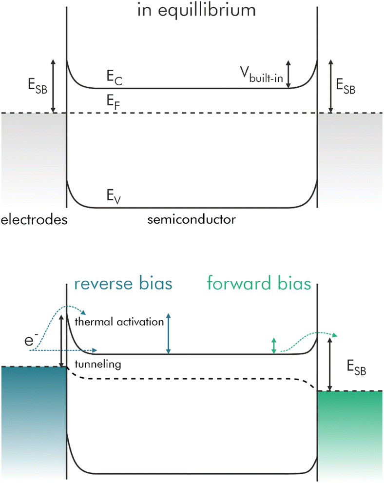 | ||
| Fig. 2 Typical band diagram of a double-Schottky barrier device in unbiased and biased condition. A potential is applied to the left contact. Electrons flow from left to right; redrawn and adapted, with permission from ref. 39. | ||
Potential barriers also occur on the contact points of individual flakes or grain boundaries of 2D-layered materials.40,41 The barrier height depends on doping and adsorbed gas species, causing additional sensitive areas on the sensor surface. A smaller flake or grain size results in a higher resistance. The influence of each of the described effects to the overall signal can vary for different sensitive materials, electrodes, and sensing environments.
Chemiresistive signal generation under ambient conditions
Many semiconducting materials have been developed to serve as a sensitive layer on chemiresistive gas sensing devices, such as metal oxides (MOx), transition metal dichalcogenides (TMDs) and carbon materials. The respective underlying mechanism is primarily dependent on the choice of carrier for the target gas. While the main response is generated by physisorption and direct electron exchange in inert carrier gases, like N2 or Ar, the mechanism in air is quite different. Here, the surface of the semiconducting material is preconditioned by the adsorption of ionized oxygen and the consequential formation of a depletion layer. For metal-oxides the charge that is transferred in the process strongly depends on temperature. In particular, more electrons are donated from the MOx to the adsorbed oxygen at higher operating temperatures. In the process, the resistance is decreased for n-type (e.g., SnO2, In2O3, ZnO) and increased for p-type (e.g., Co3O4, NiO, CuO) semiconductors, due to the altered number of charge carriers.42–44 Target gas molecules can then react with the species of adsorbed oxygen ions and change the material's resistance according to their oxidizing or reducing properties. Fig. 3 summarizes the main reactions for NO2, NH3 and acetone for measurements in inert gas (a) and in air (b). The number of electrons, which are transferred from the material by the oxidizing gases as NO2 and vice versa to the material by reducing gases like NH3 or acetone, depends on the charge of the adsorbed. Consequently, more transferred charges are leading to a higher difference in conductivity and thus a higher signal response of the sensor.42–48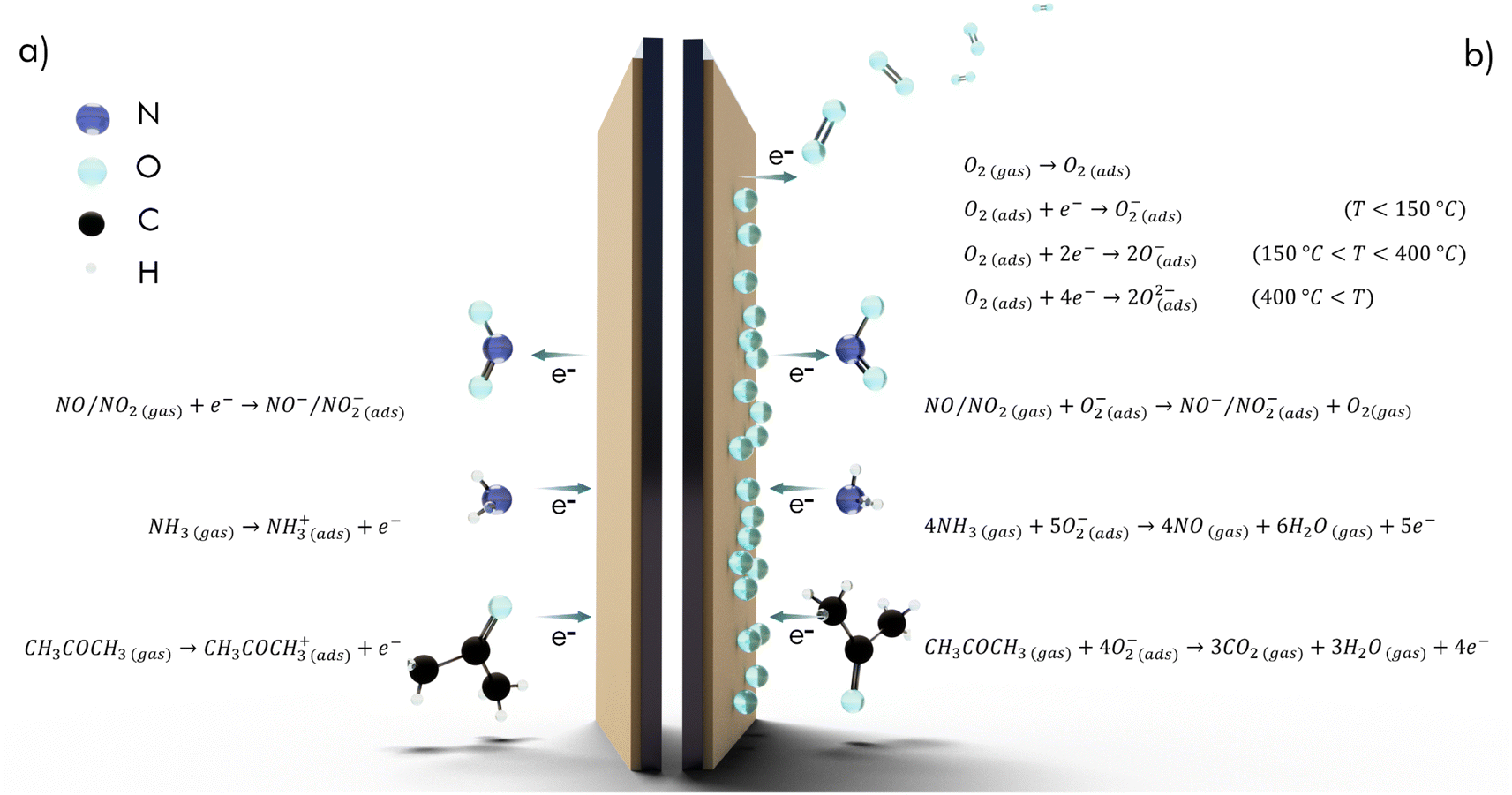 | ||
| Fig. 3 Reaction equations for NO2, NH3 and acetone on a semiconducting sensor substrate with inert gas (a) and air (b) as support gas. Temperature dependent oxygen adsorption applies to MOx sensors. | ||
Different MOx sensing substrates have been reported to enhance the sensitivity towards certain gases, improving the selectivity of the respective sensor. Many of the mostly n-type materials, including SnO2, WO3, Bi2O3, ZnO, and In2O3, showed significantly stronger responses to NO2 compared to other gases.49–53 On the contrary, p-type semiconductors like CuO have been shown to selectively sense e.g., H2S.54 NiO is reported to be selective for NH3 compared to various volatile organic compounds (VOCs),55 and Fe2O3 showed a higher sensitivity towards acetone besides ethanol, NH3 and H2.56 For some MOx, such as WO3 a temperature dependent sensitivity towards different gases was found. The material is sensitive towards NO2 at an operating temperature of 150 °C, while being most sensitive to H2S at 200 °C.57
Interactions with H2 pose a special case, as there are additional mechanisms proposed in literature, that are based on direct reactions with the sensing material. ZnO for example is reported to become reduced by H2 gas, resulting in a surface-metallization of the material, as shown in Fig. 4.43
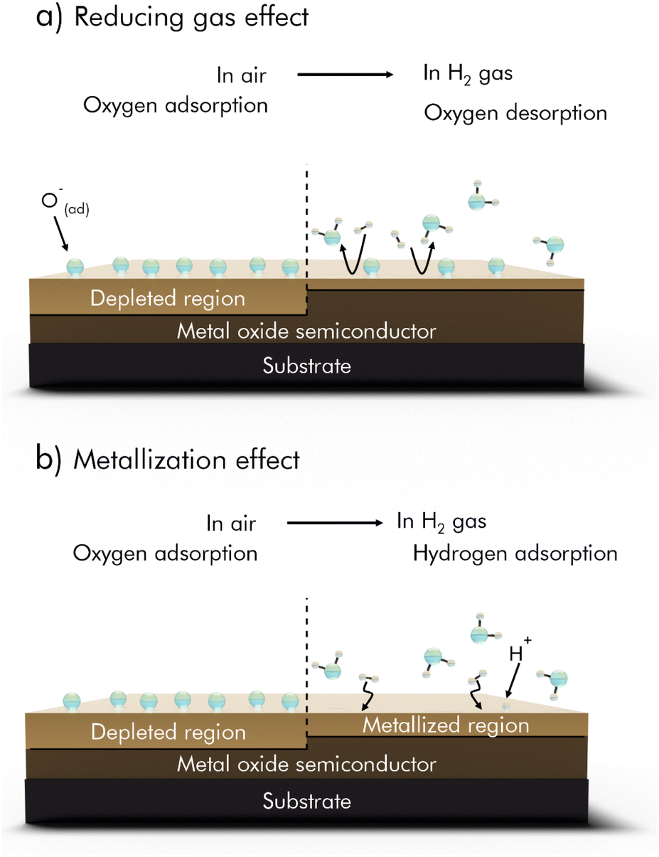 | ||
| Fig. 4 H2 sensing mechanisms of MOx based H2 sensors. (a) Reducing gas effect. (b) Metallization effect; reprinted (adapted) with permission from ref. 43. Copyright 2020 American Chemical Society. | ||
For H2 as analyte gas, decorating the sensor surface with noble metals like gold, silver, platinum, or palladium has turned out to be favorable. Two distinctive mechanisms are described, depending on the sensing ambience. In an inert atmosphere with most often N2 as carrier, molecules of the target gas get physisorbed on the noble metal's surface and change the local resistance by donating or accepting electrons. The expected response in this case is quite high, as no other interfering gases are present. The physisorption of H2 on a platinum surface in N2 ambience for example can be written as eqn (1):45
| 2Pt(s) + H2(gas) → 2PtH(s) | (1) |
For measurements in air, the sensor is again preconditioned with adsorbed oxygen, but already at lower temperature. When then H2 approaches the sensor surface, it reacts with the oxygen ions following eqn (2) and (3).45,46 The same mechanisms occur for palladium surfaces.43
| 2Pt(s) + O2(gas) → 2PtO(s) | (2) |
| 2PtO(s) + 3H2(gas) → 2PtH(s) + 2H2O(gas) | (3) |
At ambient conditions, when humidity comes into play, water molecules can occupy some of the binding sites, hindering the adsorption of H2. Further, since oxygen is still a major component in ambient air, desorption of H2 takes place at the same time, see eqn (4):45,46
| 2H2(ads) + O2(gas) → 2H2O(gas) | (4) |
This dynamic process results in a weaker response of the sensor under ambient conditions, but simultaneously a quicker recovery compared to measurements in N2 under otherwise equal conditions.45
Somehow contradictory, however, these noble metals have also been reported to be the foremost choice for doping due to a distinctive selectivity towards NO2, as well as NH3 or CO2.42,81 Reasons for differences in the sensitivities are often not discussed, thus mostly the metal itself is assumed to cause selectivity. In fact, however, its synthesis route with the resulting surface area and texture may play a huge role, if the sizes of the respective nanoparticles or nanowires differ strongly, synthesis residues remain, or different stabilizers (e.g., citrate) are added.
A promising alternative to MOx-based sensor-materials is presented by TMDs, which are mainly sulfides of Mo, W, Sn, or Ni, with the main difference of a 2D arrangement in the molecular structure. Sensing mechanisms of TMDs are usually based on a direct charge transfer from their defect sites or from p-orbitals of the chalcogenide atom. They perform well in terms of sensitivity at room temperature, but the recovery of such sensors is still challenging, limiting their long-term use or their ability for fast real-time monitoring. Additionally, TMDs suffer from strong interferences by humidity. Improving recovery by UV-illumination or heating has been attempted, but the resulting damage to their nanostructure often leads to reduced sensitivity, which is discussed in more detail elsewhere.19,58,59
Graphene-based chemiresistors
Two-dimensional carbon materials have become a popular choice as sensitive material in gas sensors. Especially graphene's favorable intrinsic properties that exceed those of MOx and even transition TMDs in terms of thermal conductivity (5000 W mK−1 at 27 °C), high room-temperature carrier mobility (20![[thin space (1/6-em)]](https://www.rsc.org/images/entities/char_2009.gif) 000 cm2 V−1 s−1), low density (0.77 mg m−2) at simultaneously high chemical stability, and mechanical durability (Young's modulus approx. 0.05 TPa) are almost predestined for miniaturized, flexible gas sensors with high sensitivity at low operating temperatures.58,60 It is noted, that the term graphene is often not used properly across literature and in commerce and seems to serve as placeholder for all types of carbon-based layered crystals. This includes its original meaning as a monolayer of nearly perfectly oriented hexagonal carbon atoms, often named pristine, but also few- or multilayered, defective structures, as in laser-induced-graphene, graphene oxide (GO), or rGO, which have entirely different electrical, mechanical, and chemical properties. In the following these types of materials are therefore referred to according to their way of manufacturing.
000 cm2 V−1 s−1), low density (0.77 mg m−2) at simultaneously high chemical stability, and mechanical durability (Young's modulus approx. 0.05 TPa) are almost predestined for miniaturized, flexible gas sensors with high sensitivity at low operating temperatures.58,60 It is noted, that the term graphene is often not used properly across literature and in commerce and seems to serve as placeholder for all types of carbon-based layered crystals. This includes its original meaning as a monolayer of nearly perfectly oriented hexagonal carbon atoms, often named pristine, but also few- or multilayered, defective structures, as in laser-induced-graphene, graphene oxide (GO), or rGO, which have entirely different electrical, mechanical, and chemical properties. In the following these types of materials are therefore referred to according to their way of manufacturing.
A key parameter for a wide variability in sensor development based on graphene derivatives is the possibility to tailor the electrical and optical properties by introducing defects in the carbon lattice, like shown in Fig. 5. Those can be for example vacancies or sp3-hybridized carbon atoms, which can additionally be functionalized e.g., by oxygen groups. Depending on the synthesis route, whether in a bottom-up approach by chemical vapor deposition (CVD),61 or by exfoliation from graphite-flakes in a variety of top-down approaches, different characteristics can be obtained.62,63
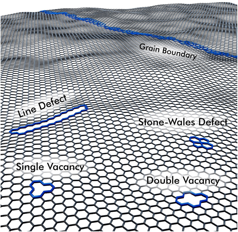 | ||
| Fig. 5 Typical structural defects within graphene flakes. Borders, which are not shown here, comprise various functional groups, such as hydroxy-, carboxy-, amine- or sulfo-groups, depending on the chemicals present during manufacturing. | ||
Important characteristics related to gas sensing include electrical resistance and the number of active sites, which are both minimal for pristine- or CVD-graphene with little to no defects. At room temperature the resistance of CVD graphene (p-type) is therefore only slightly decreased, when oxidizing gases are physisorbed on the surface and electrons are transferred from the graphene to the electron accepting gas, leaving a higher number of h+ in the lattice. Contrarily, reducing gases donate electrons to the graphene and increase its lateral resistance.
In 2012 Chen et al. studied CVD-graphene grown on copper foil for sub-ppt detection of a variety of gases, such as NO and NO2, NH3, N2O, O2, CO2 and H2O in an Ar or N2 atmosphere. The respective limits of detection (LOD) were calculated in the range from 0.16 ppt for NO and 136 ppt for CO2, while other gases had LODs in between.64 The extremely low LODs can be attributed to the minimal noise that is generated by the very low resistivity of pristine CVD-graphene (10−6 Ω cm).22,65,66 These findings inspired many researchers to investigate the huge potential of graphene and its derivatives in chemiresistive gas sensing applications. The challenge is to maintain the high sensitivity but to introduce selectivity by modifying the graphene structure. Chemical exfoliation via oxidation of graphite flakes to GO results in such a material with a great number of defects and oxidation sites,67 increasing the bandgap of the material to regions where it becomes almost insulating with basically infinite resistance.68 In its untreated form, however, due to the lack of good electrical conductance, it does not play any significant role in the development of chemiresistive sensors.60
More interesting for gas sensing applications are therefore two-dimensional carbon materials with a defect density in between the practical limitations represented by CVD-graphene and GO. Possible synthesis methods include epitaxial growth on SiC, liquid phase exfoliation (LPE), ball milling, laser inducing (LIG), and chemical reduction of GO.69
rGO has been exploited for the high number of active sites on the carbon lattice and the possible tuning thereof. Due to these defects rGO can be seen as p-type semiconducting material, so that oxidizing gases decrease and reducing gases increase the material's resistance.60 Several methods have been established to control the number of defects, which are inevitably introduced in synthesis. The group of Eigler studied the influence of temperature during the oxidation of flake graphite according to the Hummers-method to obtain less defective GO-sheets of larger size at reaction temperatures of <10 °C.70 Additional defects may be introduced by applying heat,71,72 visible or UV-illumination,73 plasma treatment,74 ion bombardment,75 or ultrasonication.72 Further control can be achieved by choice of a reducing agent. For example, hydrazine-hydrate,76 ascorbic acid,77 or sodium borohydrate,78 as well as electrochemical reduction79 were reported for processing in liquid phase. In the dry state thermal annealing in vacuum,80 the reaction with hydroiodic and trifluoroacetic acid,81 or microwave assisted reduction82 have been studied among others. These manifold options open-up access to a large number of materials with different electrical properties as well as adsorption characteristics towards different gases. Density functional theory calculations revealed that an increased oxygen content in rGO increases the electrical bandgap. A non-linear trend with values from 0.1 eV at 6.25% of oxygen to approx. 3 eV at 50% were reported.83 These oxygen groups, mainly carbonyl-, carboxyl-, hydroxyl- and epoxide-functions were also found to increase the work function of rGO from 4.2 eV up to 6.7 eV.84 Such trends may be well transferable from oxygen groups to defects in general, since both functionalities involve sp3-carbon atoms or vacancies that disrupt the sp2-lattice.85 Yet, the great diversity in materials that can be achieved by applying different synthesis routes still lacks on a standardization to allow a better comparability of different graphene-based sensor materials. Unfortunately, their exact properties, such as number of defects or bandgap, are often difficult to determine and for this reason not always communicated. The number of defects in a graphene lattice can be quantified by the intensity ratio between D-band and G-band of the respective Raman-spectrum. However, this depends strongly on the experimental conditions and further does not apply to high defect densities as in GO/rGO.75
Responses were reported to significantly increase towards the detection of O2, as a larger number of defects translates to more active binding sites for gas molecules.86 Thereby, the positive influence of defects on the performance of gas sensors is clearly demonstrated. In this context, Table 1 lists the parameters of a selection of standalone sensing devices based on carbon materials, MOx, TMDs, carbon nanotubes (CNTs), and conducting polymers (polyaniline and Poly-3,4-ethylenedioxythiophene).
| Sensing material | Test gas | Supporting gas | Operating temperature | Concentration | Response | Response calculation | Response time | Recovery time | LOD | Ref. |
|---|---|---|---|---|---|---|---|---|---|---|
| a Calculated by signal to noise ratio (3S/N). b Calculated by linear regression. | ||||||||||
| Graphene (CVD) | NO2 | N2 | RT | 400 ppt | 0.04 | Δσ/σ0 | 5 min | — | 2.06 ppta | 64 |
| NH3 | Ar | 400 ppt | 0.005 | 5 min | 33.2 ppta | |||||
| Graphene (CVD plasma-treated) | NO2 | N2 50% RH | RT | 150 ppm | 30% | ΔR/R0·100% | t 90 = 4 min | — | 18 ppmb | 86 |
| NH3 | 100 ppm | 4.5% | t 90 > 10 min | 2 ppmb | ||||||
| rGO | SO2 | Air 25% RH | RT | 5 ppm | 5.9% | ΔR/R0·100% | t 90 = 110 s | t 90 = 145 s | — | 87 |
| rGO | NO2 | N2 | RT | 0.6 ppm | 2% | Δσ/σ0·100% | t 90 = 116 s | t 90 = 169 s | 9.1 ppba | 88 |
| rGO | NO2 | Synth. Air | 150 °C | 5 ppm | 32% | ΔR/R0·100% | t 50 = 125 s | — | 0.21 ppba | 71 |
| rGO | NH3 | Dry air | RT | 50 ppm | 5.7% | ΔR/R0·100% | t 90 = 24 s | t 90 = 805 s | — | 89 |
| rGO | CO2 | Air | 100 °C | 1000 ppm | 81% | ΔR/R0·100% | t 90 = 139 s | t 90 = 600 s | 100 ppm | 72 |
| SnO2 | NO2 | Dry air | 200 °C | 0.5 ppm | 18 | R g/R0 | t 90 = 43 s | t 90 = 18 s | — | 90 |
| In2O3–ZnO | NOx | Air | 150 °C | 10 ppm | 25% | ΔR/R0·100% | t 95 = 3.5 min | t 95 = 45 min | 12 ppba | 91 |
| MoS2 | NH3 | N2 | RT | 2 ppm | 0.3% | ΔR/R0·100% | 15 s | — | 300 ppb | 92 |
| Single walled CNTs | NO2 | N2 | RT | 20 ppm | 1.5 | Δσ/σ0 | ∼10 min | ∼10 min | 44 ppba | 93 |
| PANI film | NH3 | Dry air | RT | 10 ppm | 4.29 | ΔR/R0 | t 90 = 213 s | t 90 = 98 s | 5 ppm | 94 |
| PEDOT nanowires | NO | N2 | 80 °C | 100 ppm | 0.12 | ΔR/R0 | t 95 = 5.53 min | t 95 = 3.4 min | 9 ppma | 95 |
At a first glance, it appears that purely graphene-based gas sensors give similar signal responses to a variety of different gases as MOx, TMD, CNT, and conducting polymer sensors do. All of the materials above have certain drawbacks, mainly with respect to selectivity, long response times and incomplete recovery, which are discussed elsewhere.59,96–98 Most notable, the operating temperature of MOx-based sensors is considerably higher compared to many graphene-based sensors, that work even at room temperature. The aspect of operating temperature, which is responsible for a major part of the sensor's total power consumption gives graphene a distinct advantage for the use in smartphones or watches. Also, gas sensing networks towards the IoT are a conceivable option, consisting of thousands of individual sensing devices for environmental monitoring, which quickly scales up the total power demand. In addition, the high surface to mass ratio of graphene results in smaller amounts of required material, with carbon being an easier accessible resource compared to many transition metals.
Graphene by itself allows very sensitive detection of various gases even at very low concentrations. But, due to the limited variety in adsorption sites, the issue of selectivity remains challenging and requires supplementary binding characteristics. For exploiting and tuning those special properties, it is crucial to have a fundamental understanding of the types of binding interactions for different materials and under varying conditions.
Graphene-hybrid materials
Many researchers propose hybrid materials as solution to address gas sensing at low power and ambient temperature. It is expected that benefits of two worlds can be united to a synergistic effect: on the one hand the excellent conductivity of 2D carbon materials and on the other hand the selectivity of nanomaterials made from metals, semiconductors, or organic compounds. All those materials differ in their adsorption behavior towards certain gases. One common requirement is that their electrical properties need to change and by this affect the conductivity of the material composite.Hybrid materials consist of two or more materials, usually one providing good conductivity, the others a selective interaction with certain gases. On a graphene surface, the adsorbed nanomaterial functions as a kind of mediator, by collecting information on the gas composition by specific interactions with its components. It can enhance the signal as it often provides a high surface to mass ratio which generates more binding places.
Exclusively to carbon materials like graphene derivatives and nanotubes, such functions can be covalently bound to the crystalline structure, either by nucleophilic or electrophilic substitution, condensation, or addition.99 Linkable functions can be other all-carbon materials (nanotubes or fullerenes) or a large number of different organic molecules.100–102
Many other material composites consist of a p-type semiconductor (e.g., rGO) combined with an n-type semiconductor. At their contact points, these types of composites form p–n-junctions, which are more sensitive to adsorption of gas molecules and play a major role in the overall resistance of the sensor substrate.40,103,104 In contrast to metal–semiconductor contacts a depletion layer occurs on both sides of p–n-junctions, namely an EDL on the n-doped, and an HDL on the p-doped side. This results in a potential barrier for electrons as well as holes. Differences in the bandgap of the materials cause the presence of discontinuities within the junction (ΔEC, ΔEF). The depletion layer is usually not symmetrical, and its thickness on either side depends on the permittivity of the material. In Fig. 6 a typical band diagram of a p–n-junction is shown.
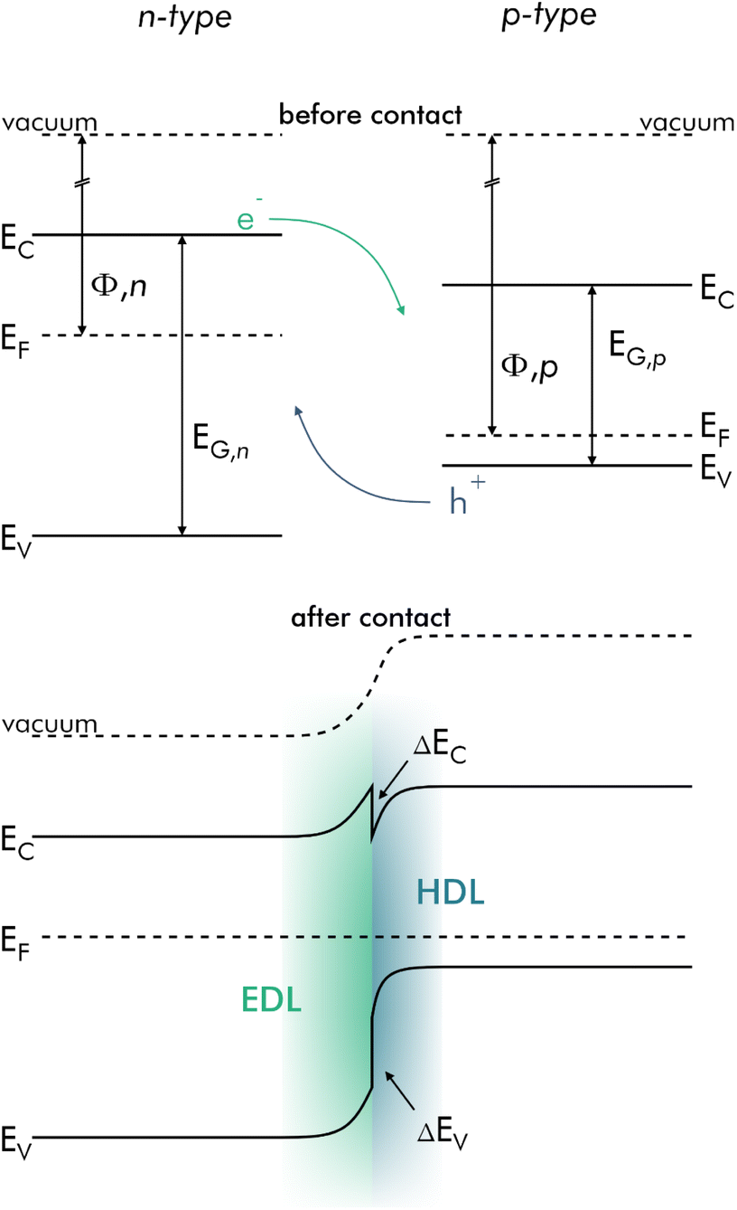 | ||
| Fig. 6 Band diagram of a typical p–n-junction in equilibrium before and after making contact. EDL and HDL are formed after electron–hole recombination during Fermi level alignment. | ||
These materials can be engineered or functionalized individually to further increase the variety of intrinsic properties. In graphene for example doping is possible using boron (p-doping) or nitrogen (n-doping), which results in changes of its Fermi level EF,105 and defect engineering to tune the bandgap EG and work function Φ.83,84 Functionalization on the other hand mostly involves small organic molecules, that are either bound covalently to the graphene's carbon lattice or held in place by π-interactions.106 For the latter, porphyrins or phthalocyanines have been used extensively as they are able to bind different metal atoms, which in turn act as preferred adsorption sites for gas molecules. These make it quite easy to obtain a high diversity without complicated procedures.107
Decoration with noble metals has been reported regularly, to selectively enhance the sensitivity. Gold nanoparticles for example have been shown to enhance signal responses towards H2, CO, CO2, and NH3, as well as CH4.47,98 Graphene decorated with silver or platinum nanoparticles was used for detection of NH3 and H2.45,47,108 Especially towards H2 sensors, palladium decoration has shown good sensitivity enhancements, because of its affinity to form hydride bonds.109 These hybrid materials are either prepared separately and then linked together or synthesized in situ. Here, the graphene's catalytic effect on the reduction of noble metal salts offers a convenient way of synthesis, as the nanoparticles tend to nucleate directly on its surface, making further binding-chemistry unnecessary.110 The obtained decorations, however, are not necessarily spherical in shape. For example, Shin et al. reported electrodeposited palladium nanoclusters on graphene with a flower-like morphology, which results in an increased surface area for H2 to bind to.111 A strategy to further optimize metal decorated sensing substrates can be to use metal alloys. In a specific case, nickel–palladium bimetallic nanoparticles enhanced the performance of a graphene-based resistivity-type H2 sensor and additionally reduced the hysteresis behavior of the Pd-graphene hybrid.112 Because noble metals are more conductive than rGO or other 2D-layered materials at room temperature it is however possible to overload the sensor with metal particles. In Fig. 7 this case is illustrated for a H2 sensor loaded with different proportions of palladium.113
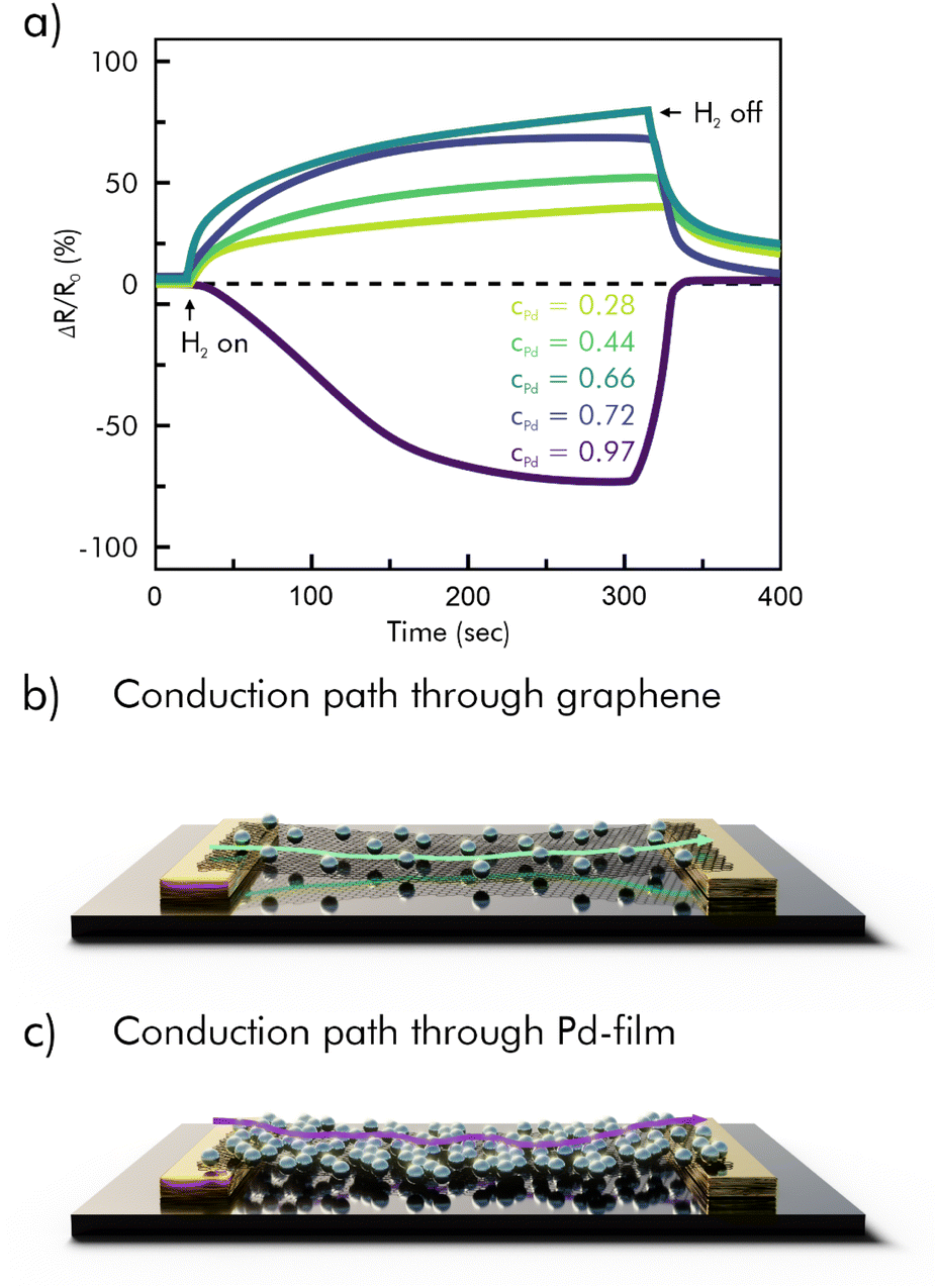 | ||
| Fig. 7 a) Relative resistance response (shown in percent) of PMMA/Pd/graphene hybrid sensors with different values of cPd on single-layer graphene as a function of time, exposed to 2% H2; (b and c) schematic representation of the conduction path through graphene and Pd; reprinted (adapted) with permission from ref. 113. Copyright 2015 American Chemical Society. | ||
Considering that junctions, functionalizations, and decorations only occur locally, no change of the remaining carbon surface and its affinity towards interfering gases is expected. The sensitivity towards a certain gas may therefore be enhanced, while the response to other gases remains the same, a behavior that requires attention and targeted research. In the case of very reactive gases, like NOx, NH3, or H2S this effect can be quite strong and in comparable concentrations even overpower the response to the intended target gas.114
Composites with polymers can be classified by their purpose on the sensor. On one hand, conducting polymers are used to act as an additional sensing substrate or to enlarge the overall surface area of the sensor. Here often conducting nanofibers based on polyaniline (PANI) or poly-3,4-ethylene-dioxythiophene (PEDOT) are used, because they can respond to gas adsorption (most frequently NH3 or H2S) by themselves and provide a large surface area.115 A greatly enlarged surface area, however, can result in significantly higher noise due to more unspecific binding sites. Also, the dynamic range is increased, which allows for higher concentrations to be measured, but in turn reduces the sensitivity of the sensor. Therefore, a trade-off needs to be made between the higher number of binding sites and noise.
The other common usage of polymers comes in the form of coating over the entire sensor. Porous polymers, permeable only to molecules of a suitable size add a sieve effect to exclude many interfering larger molecules. This class of composites has been used for sensing small molecules like H2 in complex mixtures, or small VOCs. In literature for example coatings with polymethyl-methacrylate (PMMA), polyvinylidene-fluoride (PVDF) and polytetrafluoroethylene (PTFE) are reported.113,116 A complete compendium on functionalization strategies for graphene can be found elsewhere.117
Environmental gas sensors
In the environmental monitoring sector, it is desirable to improve the sensors' usability by miniaturization as well as large scale manufacturing and operation at affordable running costs. The state of the art to measure air pollution, however, is to set up bulky and expensive measurement stations. As an example, there are around 400 of such stations throughout Germany, five of which are located in the Bavarian city of Munich.118 Their use is therefore limited because the network is not dense enough to capture air pollution for individuals. In contrast the German Meteorological Service (DWD) is running 180 full-time and 1734 part-time weather stations.119 For surveilling the effects and dangers of climate-change it was recommended that ships and airplanes also be equipped with such sensors to serve as individual, mobile monitoring stations, tackling the discrepancy between calculated and only sporadically measured concentrations, e.g., of CO2 emissions.120Depending on the field of application the demands on a sensor vary and require different solutions. For environmental gas sensing, some analytes such as greenhouse gases are present in relatively high concentrations (CO2 at 410 ppm and CH4 at 1.7 ppm) and small changes need to be monitored over a long time at sometimes harsh conditions. The situation is different for toxic gases like, NO2, SO2, CO and NH3, which mostly occur in trace amounts.121 These gases need to be monitored very sensitively in a usually narrow dynamic range around very low concentrations. Further, the targeted gases must not interfere with one another on the sensor at different levels of humidity to ensure correct data acquisition on the atmospheric composition. For usage within IoT concepts, huge numbers of such sensors would operate day and night, making low power consumption a very relevant characteristic. This demands miniaturization and low operating temperatures.
On the contrary, response and recovery times are less relevant, as detecting changes in most gas concentrations in the environment is not as urgent. Devices that can deliver one precise and reliable measurement every 15 to 30 minutes are in this case sufficient.
A great deal of attention was given to NO and NO2, as they are highly toxic even in small amounts and their concentration in the atmosphere has been increasing over the last years, especially in urban areas.122–125 Naturally occurring NO2 for example is generated in the troposphere by oxidation of N2 in lightning bolts or by UV radiation, however, much is also manmade as an exhaustion product of combustion processes and welding units.126–128
Due to its atmospheric occurrence in trace amounts and low assessment thresholds10,121 a high sensitivity and especially low LODs are essential and must hold up in ambient and sometimes even harsh conditions.
An extremely low LOD of 5 ppb could be achieved using an n-type hybrid material consisting of SnS2 and rGO.103 While a pristine SnS2 sensing material showed no significant signal towards NO2, due to its low conductivity at RT, rGO enhances the sensing performance drastically by forming charge transfer pathways. These allow charge travelling from the SnS2 to rGO which is then transported along its sp2 carbon structures, resulting in fast and strong variation in the hybrid-material's resistance. Density functional theory calculations further revealed a closer adsorption distance of NO2 towards rGO in the presence of SnS2, which makes it possible to attach more NO2 molecules to the surface. Under illumination at 650 nm (1 mW cm−2) the proposed sensor exhibited a signal response of 650% to 1 ppm of NO2 in synthetic air at room temperature (S = I − I0/I0 × 100%). The sensitivity enhancement of around five-fold was attributed to electron–hole pairs, which were generated and separated in the conduction and valence band of the n-type SnS2. The photoexcited holes combined with O2− and the resulting photo-desorption of physically adsorbed oxygen species lead to a reduced barrier height and an increase in electron charge carriers. By increasing the amount of rGO in the hybrid material, the semiconducting behavior is shifted to p-type. Because of the narrower bandgap of rGO and its lower affinity towards oxygen, illumination has little effect on the signal response of the p-type sensor, which is reported to be 47% at equal conditions. The significantly lower noise, however, improved the theoretical detection limit down to 1.10 ppb. Both sensors showed a high selectivity against the reducing gases H2, NH3, CH4, ethanol and H2S, as well as independence from RH in the range between 30% and 90%, as shown in Fig. 8. Furthermore, it is shown, that the recovery of the n-type sensor is quicker and drift-free, while it seems, that the p-type material does not recover by itself.103 However, this is not a general conclusion, as such trends have also been shown to go into the opposite direction, where p-type rGO was superior with respect to response and recovery compared to its n-doped counterpart.129
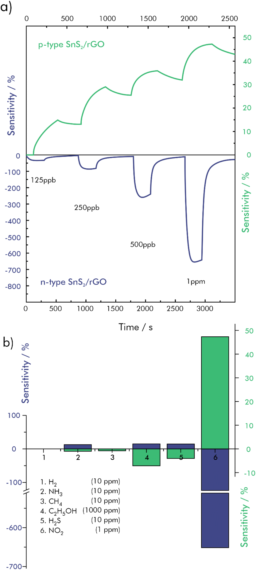 | ||
| Fig. 8 Gas sensing performances of n-type SnS2/rGO and p-type SnS2/rGO; (a) dynamic response–recovery curves towards NO2 at concentrations from 125 ppb to 1 ppm at RT, (b) cross sensitivity of NO2 (1 ppm) towards H2 (10 ppm), NH3 (10 ppm), CH4 (10 ppm), C2H5OH (1000 ppm) and H2S (10 ppm); redrawn and adapted, with permission from ref. 103. | ||
Signal drift is a non-negligible parameter for long-term monitoring applications. To account for drifts and other possible interfering factors on the sensor, like air pressure and ambient temperature, suitable reference materials are of great importance and require targeted research.
In another approach, shown in Fig. 9, a flexible, stacked sensor geometry including rGO and zinc-oxide nanorods (ZnO NR) was used to fully reversible detect NO2 down to a concentration of 40 ppb in dry synthetic air.130 Here rGO also acts as the main charge transport layer, while the ZnO NR serve primarily as a gas reaction layer. The sensor was shown to be significantly less sensitive towards SO2, NH3, acetic acid, acetone, and ethanol. The overall resistance of the sensing material, however, changed drastically with increasing humidity, although the relative signal did not. Nevertheless, this circumstance complicates things for monitoring purposes.
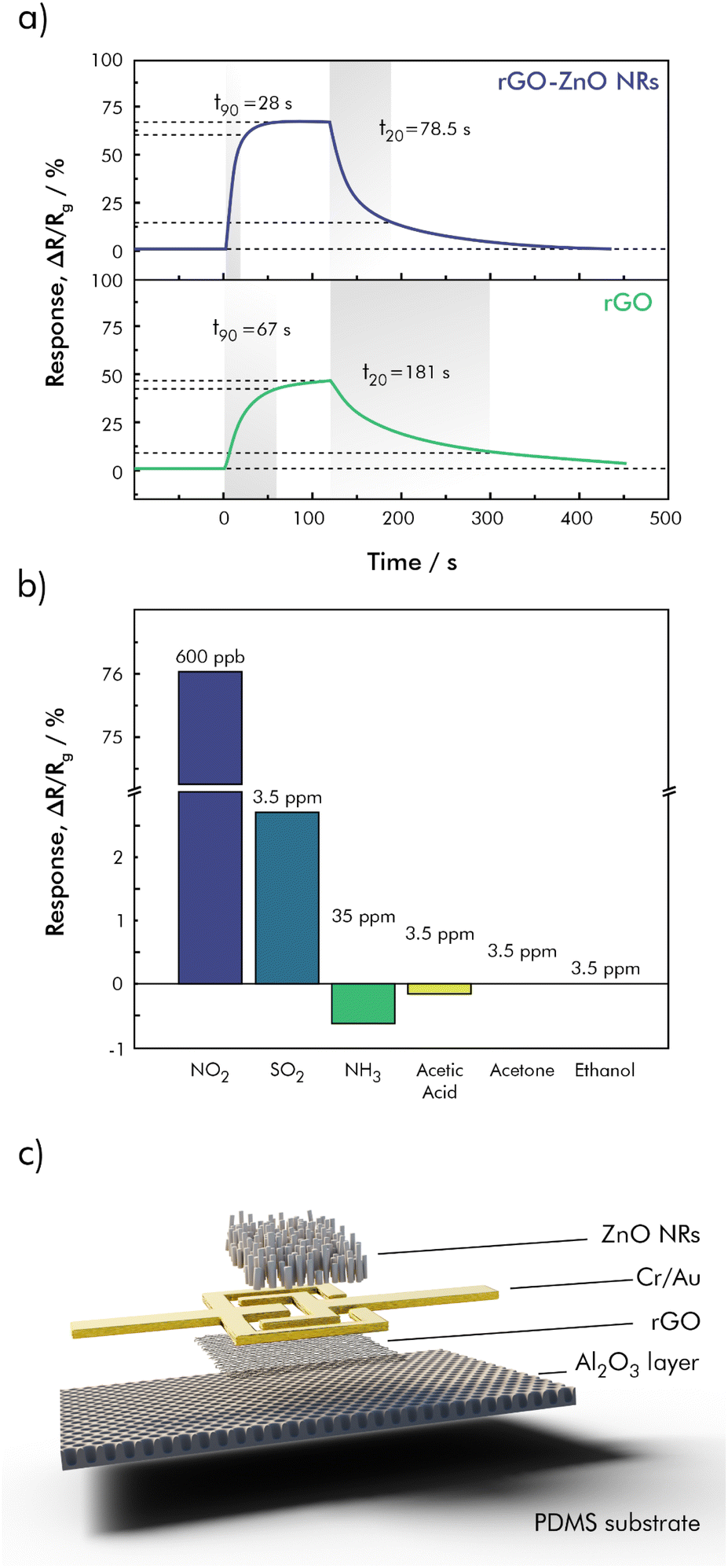 | ||
| Fig. 9 (a) Dynamic response recovery curves from rGO and the rGO-ZnO NR towards NO2 at a concentration of 400 ppb, (b) selectivity test using NO2 (600 ppb), SO2 (3.5 ppm), NH3 (35 ppm), acetic acid (3.5 ppm), acetone (3.5 ppm), and ethanol (3.5 ppm); (c) sensor geometry of the stacked rGO-ZnO NR hybrid sensor; redrawn and adapted, with permission from ref. 130. | ||
As a way to achieve better selectivity, sensor surfaces have been covered with semipermeable membranes, to eliminate the influence of interfering gases and humidity in particular.131 The here proposed, rather simple sensor-design, based on laser-induced graphene, covered with a polydimethylsiloxane (PDMS) membrane, showed good selectivity towards NO and NO2, however, with a significantly lowered response. These membranes may also raise response- and recovery-times because of a slower diffusion of the target gas towards the sensitive surface, but for the use in environmental sensing systems this seems to be a reasonable tradeoff.
A mechanism for the quantification of NO in N2 at room temperature on a rGO-based sensor, modified with hemin-complexes was proposed, that involves the formation of covalent Fe–C bonds, that act as electron-transport channels.132 An understanding of such mechanisms is crucial for the fabrication of selective sensors now and in the future.
The monitoring of some greenhouse gases is more challenging. Due to the high similarity of CH4, CO2, and N2 molecules in their chemical properties, a sensing material, which is selective and sufficiently sensitive towards CH4 or CO2 is still needed. So far, receptor materials for chemiresistive determination of those gases lack the required LOD and selectivity to be applied under ambient conditions.113,133–135 In this case other types of gas sensors, such as photoacoustic devices, are superior at the moment and further research is necessary to develop suitable hybrid materials.
Gas-leakage warning systems
While environmental sensors are operated in the open field, warning systems for toxic gases are more often deployed indoors and near gas containers and pipelines. To allow timely countermeasures and evacuation in the case of a gas leak, a quick response of the installed sensor device is the most important aspect. Together, response and recovery determine the time such a sensor needs to come into equilibrium with changing gas concentrations. Next, the limit of detection of the sensor device must match concentrations that are either legally determined as assessment thresholds by state authorities or listed as maximum workplace concentrations for a variety of harmful gases, usually in the range of ppb to ppm.11,136 For flammable, but otherwise non-toxic H2, sensors must be able to detect concentrations up to 4% in air, which is the critical ignition concentration.137 The aspect of sensitivity is less relevant, compared to environmental monitoring, as gas concentrations tend to increase drastically in close proximity to a leak.Depending on their location, these warning systems may be operated continuously or only over the duration of a workday. In any case they benefit from lower power consumption and miniaturization.
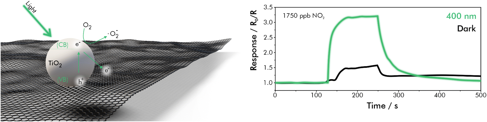
With regards to workplace safety, warning systems for NOx gas may find their purpose for example in welding workshops or other metal processing facilities. One potential sensor for such an application was made using a hybrid-material of TiO2 and graphene, as depicted in Fig. 10, which was synthesized via the sol–gel method.138 An approach in which TiO2 and graphene were annealed together during synthesis showed a significantly improved sensing performance compared to a synthesis, where only TiO2 was annealed and then mixed with graphene or compared to TiO2 only. This improvement was attributed to the smaller particles and related higher surface area. Further sensing improvement was achieved by illumination with a 400 nm LED light source (180 mW), which resulted in a two-fold increase in response up to 3.14 (R0/R) at 1750 ppb of NO2. The optimized sensor was tested in synthetic air at room temperature and a RH of 40%. Response to NO2 was measured in a range from 70 to 1750 ppb, with a theoretical LOD of 50 ppb, which was calculated by a signal-to-noise ratio of S/N = 3. Because the dynamic range of the sensor does not include the low concentration of NO2 in the atmosphere (∼20 ppb) it is not suitable as a device for its environmental monitoring. However, assessment thresholds (160 ppb), alert thresholds (330 ppb) and maximum workplace concentrations (790 ppb) certainly lie in the dynamic range of the sensor.10,11 Further, the short response-time (t90, at which 90% of the saturated response is reached) of 35 s makes it a suitable candidate for integration in toxic-gas warning systems.138
 | ||
| Fig. 10 Sensing mechanism and dynamic response–recovery curves of GTiO2S towards 1750 ppb of NO2 in dark and illuminated operating mode; redrawn and adapted from ref. 138. | ||
An even faster response was achieved with a three-component hybrid of Pd-functionalized CuO/rGO. Here, a t90 of only 10.7 s was achieved, when exposed to a concentration of 10 ppm of NO2 (R0/R = 64.2). Synthetic air was used as carrier with a RH of 25%. The authors attributed the high as well as quick signal response to the porous structure of the material and gas paths, which are induced between the heterojunctions of CuO and rGO. Additionally, an enlarged specific surface area by Pd-functionalization is proposed to accelerate the transport of charge carriers through the sensing material. The Pd–CuO/rGO sensor and its predecessors were further tested for cross sensitivity against NH3, H2, CO and SO2. No significant interference from this selection of reducing as well as oxidizing toxic gases was found.139
Not toxic, but potentially hazardous, H2 is widely regarded as a promising candidate for energy storage and sustainable fuel. Consequently, the development of H2 sensors is important to ensure safety while handling the explosive gas. In the atmosphere, H2 is present in a very low concentration of 0.55 ppm,121 however, only at higher concentrations between 4% and 75% in air the gas mixture becomes explosive.137 For the integration in warning systems, the concentration range of interest lies therefore below 4% as an upper limit, with relatively moderate LODs with respect to the individual demands. Because hydrogen is the lightest element on earth, H2 rises through the atmosphere very quickly, which makes is difficult to detect and locate a leak in the open. Here the LOD needs to be much lower.
rGO decorated with Pd-nanoparticles has been studied for its usability as a sensitive substrate for H2 under varying influences like gas concentration, temperature, humidity, and UV illumination.82 The rGO/Pd material was sensitive towards H2 in a concentration between 0.2% and 1%, and responded differently depending on the temperature, as shown in Fig. 11a. In dry synthetic air the signal response reached a maximum of 14.9% (S = (R − R0)/R0 × 100%) at 100 °C, when exposed to 1% of H2. Response- and recovery-times were improved by a higher operating temperature, as well as exposure to UV-light (365 nm at 8.9 μW mm−2), however, strongly dependent on the concentration (Fig. 11b).
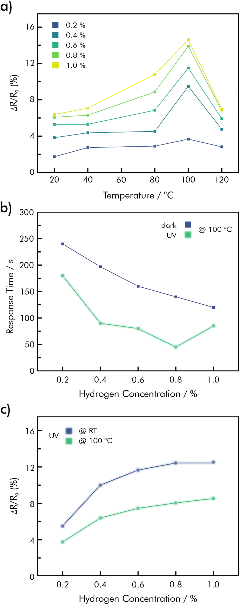 | ||
| Fig. 11 Hybrid Pd/rGO sensing performance (a) temperature-dependent responses towards H2 at different concentrations; (b) effect of UV-illumination on response times as a function of H2-concentration at 100 °C; (c) signal responses under UV-illumination at RT and 100 °C as a function of H2-concentration; redrawn with data from ref. 82. | ||
At the suggested optimum working temperature of 100 °C humidity was shown to have a positive influence on the signal response. When the sensor was exposed to 0.5% of H2, with varying levels of humidity, the signal response increased at 10% RH due to the presence of hydroxy active sites, that support electric charge transfers and the formation of hydronium cations from the water molecules, improving the material's conductivity.140 At higher levels of humidity, however, water molecules cannot compete with H2 to access the sensing surface as effectively due to their size. The electrical properties of the sensor remain therefore constant at higher temperatures.141
Interestingly, UV-illumination proved to have different effects on the sensing properties of the material. On the one hand signal response was enhanced when operating the sensor at RT, but was decreased at 100 °C, see Fig. 11c. This behavior may be ascribed to an acceleration of the desorption rate, more than the adsorption rate, due to the Langmuir adsorption probability phenomenon.142,143
At all temperatures response/recovery-times were improved significantly by UV-illumination. For the application in real-time monitoring and warning systems a tradeoff is often necessary. In this case the lowered signal response and higher power consumption at 100 °C under UV-illumination may be accepted for the improvement of response- and recovery-times.
For a safe and easy-to-handle storage medium for H2 as an energy carrier, the power-to-ammonia approach has been discussed. On the one hand the hydrogen content of ammonia is higher than for water, and on the other hand nitrogen as feedstock is more easily accessible compared to CO2 for the power-to-gas process towards CH4 or methanol, which either requires point sources of CO2 or extraction from the atmosphere at a much higher energy consumption.144,145 Consequently, NH3 sensors may not only be useful in ammonia plants and in agriculture but in future fuel stations as well.
Through the example of an NH3-sensitive hybrid material combining In2O3 ceramic nanofibers (NFI) and rGO, an elegant way to improve response- and recovery-times without heating or illumination is shown.146 The sensor was tested against concentrations of NH3 ranging from 1–60 ppm in synthetic air at room temperature and 30% RH. In a no-flow setup an AC-voltage was applied to the NFI-rGO sensor, and the signal response was evaluated through a frequency sweep from 1–106 Hz (Fig. 12a). The strongest response was found at a frequency of 104 Hz, which is related to the charge transfer resistance at the sensitive layer interface, that was previously determined by impedance measurements. By applying an AC voltage of 75 mV at a frequency of 104 Hz an extremely short response-time of t90 = 17 s was achieved, with a full, but slow recovery (Fig. 12b). An interference study, against a selection of VOCs was conducted and showed good selectivity (Fig. 12c).146
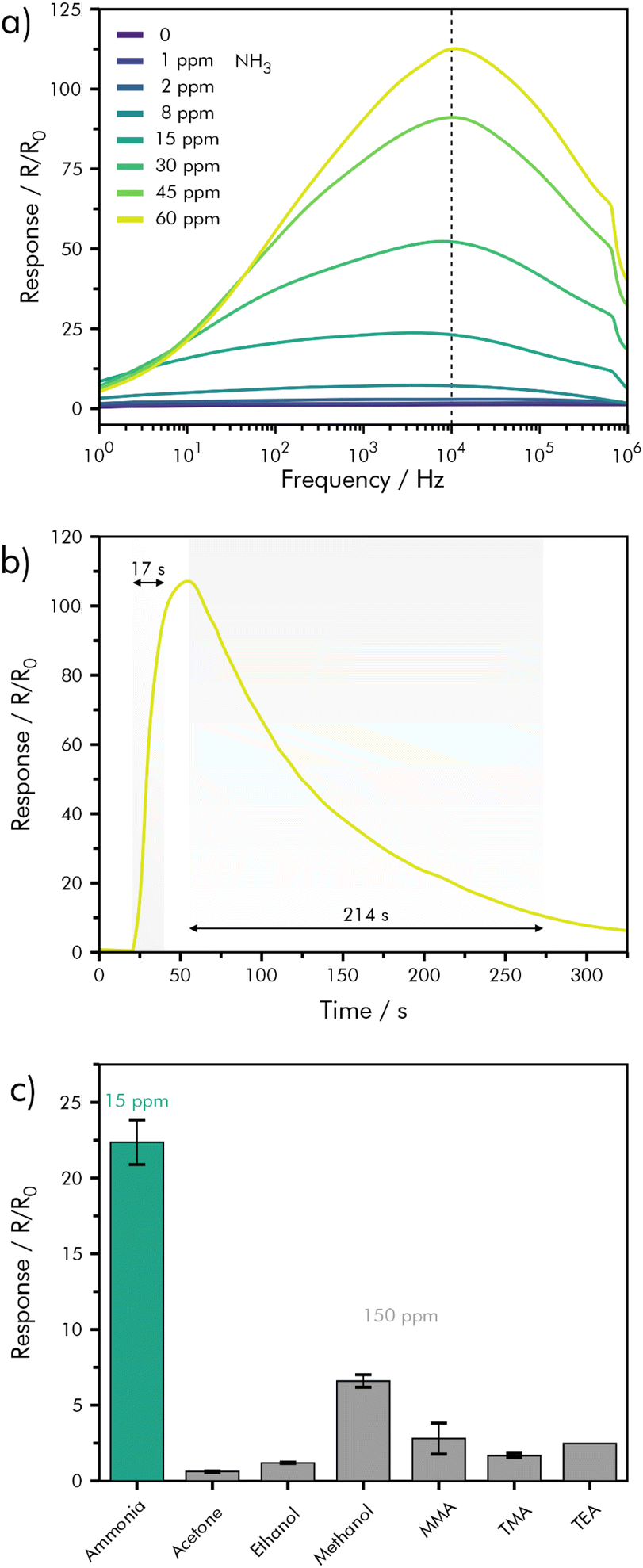 | ||
| Fig. 12 Hybrid NFI-rGO sensing performance (a) relative response variation as a function of frequency for NH3 concentrations from 0–60 ppm; (b) dynamic response–recovery curve for exposure to 60 ppm of NH3; (c) cross-sensitivity between NH3 (15 ppm), acetone, ethanol, methanol, monomethylamine (MMA), trimethylamine (TMA) and triethylamine (TEA) (150 ppm); redrawn and adapted, with permission from ref. 146. | ||
In contrast to conventional DC resistance, which is sensitive to strong adsorption and desorption processes on the sensing surface, AC measurements give access to phase change responses, that are sensitive to weak but quick adsorption and desorption of gas molecules above the sensing surface. As such they respond faster to changes in the gas composition and suffer less from baseline drifts.19,147 The large dynamic range of the sensor and its low LOD of 44 ppb, considering a signal-to-noise ratio of S/N = 3, make it a suitable candidate for many gas-sensing applications from detecting leakage of NH3, to environmental monitoring and medicinal breath analysis.
Healthcare and breath analysis
Healthcare and diagnostics present yet another case and the demands to gas sensors differ from those in environmental and surveillance applications. One of the best known commercially available gas sensors for human breath is used for estimating the blood alcohol content by various methods, including infrared spectroscopy, electrochemical oxidation, or MOx-based sensors. Their accuracy is however strongly affected by measurement parameters, like breathing patterns, and interference from other VOCs.148,149Nevertheless, analysis of human breath may offer a non-invasive alternative to many time-consuming and cumbersome medicinal techniques, e.g., hemograms and biopsies. Disease patterns that were reported to profit from early recognition by breath analysis include kidney disorder or ulcers caused by certain bacterial infections, indicated by highly elevated amounts of exhaled NH3,14,150,151 acetone (an indicator for diabetes mellitus),152,153 or several other gases and VOCs attributed to a patient's health status.154 These biomarkers are however only present in trace concentrations, demanding outstanding sensitivity at low LODs. Further, because breath contains more than 900 different VOCs,154,155 good selectivity is also an essential requirement for a reliable diagnosis. Accordingly, long response times of several minutes may be accepted for the sake of accuracy. In contrast to sensors for monitoring applications, these types of diagnostic devices would most likely be operated on demand. Power consumption and size are therefore irrelevant except for transportation and operation at the point of care.
Chemiresistive sensors for biomarkers such as NH3 have been shown to be suitable for operating in environmental monitoring and in particular toxic gas surveillance.146 Their sensing capabilities may be applied to the field of healthcare as well. Selective sensing of VOCs on the other hand proves to be more difficult, as their chemical composition and binding characteristics often vary little or not at all. The information they carry about a patient's health status, however, may be very different.
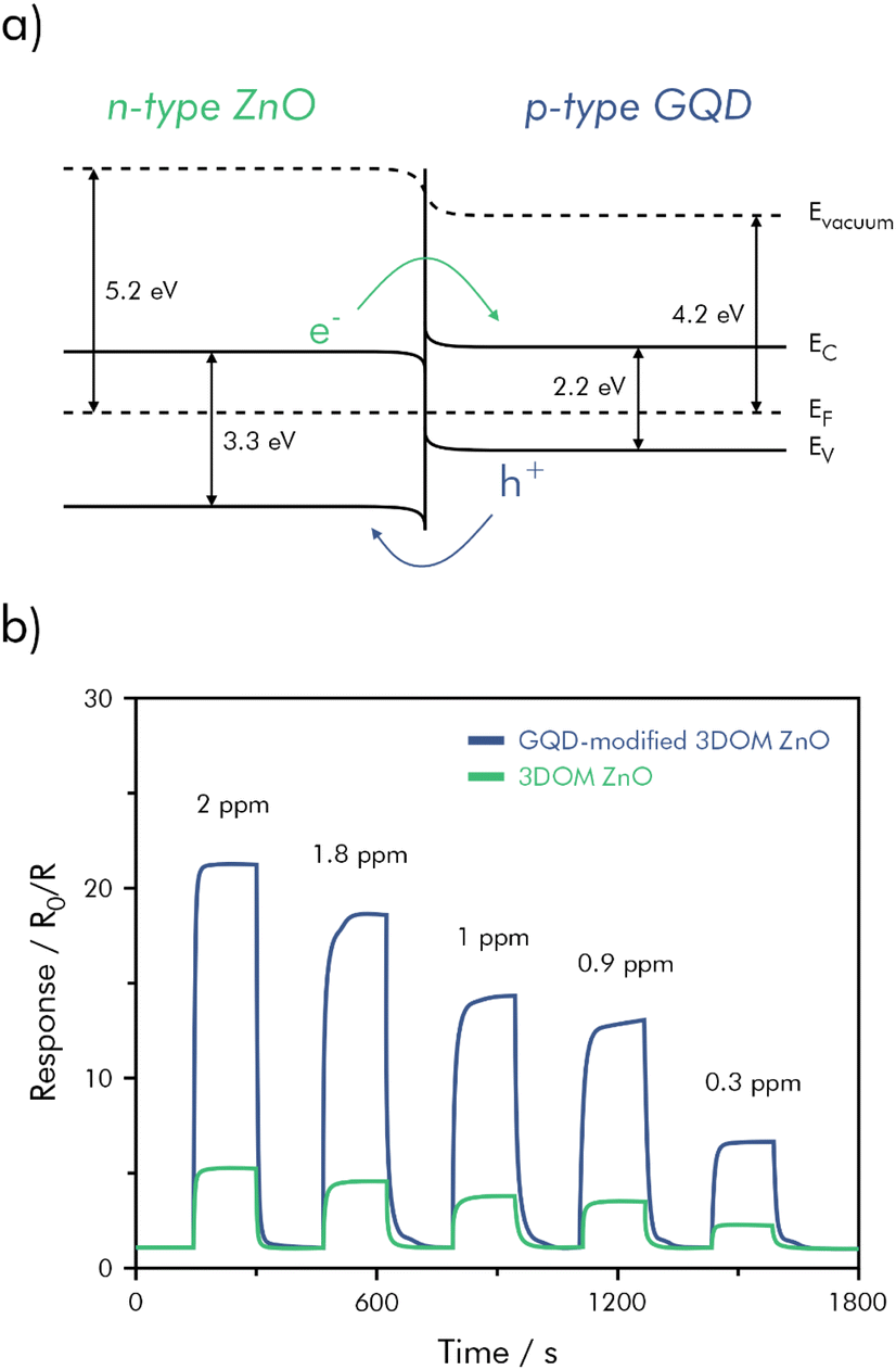
Specifically developed for diabetes diagnosis, a sensing material of three-dimensional ordered mesoporous (3DOM) ZnO functionalized with graphene quantum-dots (GQD) showed good sensitivity and selectivity towards acetone vapors, especially when compared to the non-functionalized ZnO.152 A higher sensitivity was attributed to the formation of p–n-junctions, shown in Fig. 14a. The hybrid-material was coated onto the surface of a ceramic tube substrate as a paste to form a sensing layer of about 500 μm on a pair of Au electrodes on each side. The tube was annealed at 350 °C for 3 h and additionally aged at a 5 V heating voltage for 24 h. In a non-flow environment under laboratory conditions (22% RH, 20 °C), the sensor exhibited a very quick response and recovery of t90 = 9/16 s and a high signal response (S![[double bond, length as m-dash]](https://www.rsc.org/images/entities/char_e001.gif) R0/R) of 15.2 when exposed to 1 ppm of acetone in air (Fig. 14b). The LOD was calculated to be as low as 8.7 ppb (S/N = 3); however, the experimental LOD was determined to be 50 ppb, which includes the healthy exhaled acetone concentration of 300–900 ppb.152,156 On the contrary, acetone concentrations in the breath of diabetes patients were found to exceed 1.7 ppm.157 The significantly higher power consumption, due to the high operating temperature of 320 °C does not impede the sensor's usability, as it would be the case for monitoring applications. On the other hand, the high temperature neither eliminates the signal dependency on RH, which is around 80% in exhaled breath. Along with humidity the sensor's responses against 5 ppm of NO2, H2S, NH3, toluene, ethanol, isopropanol, and NO were tested indicating an improvement in selectivity for the hybrid material.
R0/R) of 15.2 when exposed to 1 ppm of acetone in air (Fig. 14b). The LOD was calculated to be as low as 8.7 ppb (S/N = 3); however, the experimental LOD was determined to be 50 ppb, which includes the healthy exhaled acetone concentration of 300–900 ppb.152,156 On the contrary, acetone concentrations in the breath of diabetes patients were found to exceed 1.7 ppm.157 The significantly higher power consumption, due to the high operating temperature of 320 °C does not impede the sensor's usability, as it would be the case for monitoring applications. On the other hand, the high temperature neither eliminates the signal dependency on RH, which is around 80% in exhaled breath. Along with humidity the sensor's responses against 5 ppm of NO2, H2S, NH3, toluene, ethanol, isopropanol, and NO were tested indicating an improvement in selectivity for the hybrid material.
In a final experiment the assembled sensor device, was exposed to exhaled breath samples of healthy subjects and samples of simulated diabetes (breath with 2 ppm of acetone added). The samples were collected through a tube filled with a molecular sieve to further reduce the influence of humidity on the sensing performance. In this setup, the sensor was able to distinguish between samples of healthy subjects and those with simulated diabetes.152
A total of nine separate sensors for different VOCs, which are regarded biomarkers for lung cancer were described using a molecular imprinted polymer (MIP) as recognition element on a Prussian blue doped rGO layer.158 The sensor was prepared using pyrrole as monomer, mixed with 0.5 mM of the target biomarker. The polymer is deposited by means of cyclic voltammetry from an aqueous phosphate buffer solution onto the modified graphene layer, which is supported by chromium-coated silicon. The target biomarker is then removed by washing with ethanol, leaving the respective MIP. The MIP is contacted to a custom printed circuit board. A sensor scheme is shown in Fig. 13.
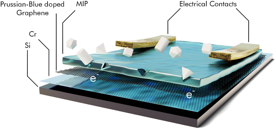 | ||
| Fig. 13 4-layer structure of the VOC sensor with electrical contacts to be connected to a printed circuit board, target molecules are trapped inside the cavities of the MIP and the extra electron is transferred to the graphene layer causing a resistance change; redrawn and adapted, with permission from ref. 158. | ||
 | ||
| Fig. 14 (a) Proposed energy band diagram of the p–n-junction at the interface of 3DOM ZnO and GQD; (b) dynamic response curves for 3DOM ZnO and GQD-modified 3DOM ZnO in the concentration range 0.3–2 ppm acetone; redrawn and adapted, with permission from ref. 152. | ||
Instead of using conventional DC voltage, an AC resistance was measured followed by a conversion to DC voltage at the output. In this way nine sensor-setups with different MIPs were able to detect butyraldehyde, tetrahydrofuran, acetonitrile, heptane, hexanal, benzene, pentane, 2-butanone, and furan at concentrations in the range of 1–20 ppt, showing a linear behavior. An interference study of the pentane-MIP against heptane, hexanal and furan showed promising results.158 Information on sensitivity, response- and recovery-times, and LOD, however, is not given, and it is stated, that the dilution process of the analytes does not follow analytical standards.
Advanced readout techniques
In the development of chemiresistive gas sensors the issues of high sensitivity and low detection limits have been the most addressed sensing parameters and show great improvements even under ambient conditions. Hurdles which need to be overcome in bringing this technology to market and which still require further research include long response and recovery times, low stability and durability, high operating temperatures, as well as insufficient selectivity.Attempts to reduce high operating temperatures, especially for MOx- or TMD-based chemiresistors by designing receptor materials based on graphene-nanocomposites have already been shown to be very successful and gas sensors, which are operated even at room temperature now constitute the majority of publications in this field of research. On the other hand, issues of long-term stability and durability of sensor devices still require attention and targeted research.
Enhancing parameters like response- and recovery-times and selectivity may however prove more difficult, especially when the chemistry itself reaches its limits. Therefore, looking towards measurement techniques and data-processing could hold the key to future milestones in multigas sensing.
For example, it was shown that response and recovery times could be significantly reduced without any baseline drift by conducting resistance measurements using AC instead of DC voltages.19,146,147 By doing so for many different frequencies also much higher information content can be extracted from a single measurement. Further, AC measurements show responses to weak adsorption and desorption processes of gases above the sensing surface, while conventional DC resistance changes are sensitive only to strong adsorption and desorption directly on the sensor. Evaluating the signal responses for a variety of frequencies may offer a route to achieve selectivity via principal component analysis (PCA), pattern recognition or machine learning. In this regard, electrochemical impedance spectroscopy has been reported as a highly sensitive technique to measure the performance of gas-sensing devices. Specifically, it is an efficient tool to measure and properties such as the gain bulk and boundaries or identify surface mechanisms, e.g., at the interface between electrode and sensing layer.159 Apart from that, the information content of impedance spectroscopic measurements is considerably higher compared to simple changes in resistance, which provides more reference points for pattern recognition. Detailed information on Impedance spectroscopic gas sensing can be found elsewhere.160
Similar to the mammalian olfactory system, also distinguishable responses from an array of independent sensors towards various gases can be processed to discriminate between analytes in complex mixtures (see Fig. 15).19,161,162 By feeding the signal responses of four sensor substrates (SnO2, In2O3, WO3, CuO) to a convolutional neural network (CNN), it was possible to classify and quantify CO, NH3, NO2, CH4, and acetone with an accuracy of 98% within the validation set. Through principal component regression concentrations could be predicted within a 10% error range.162
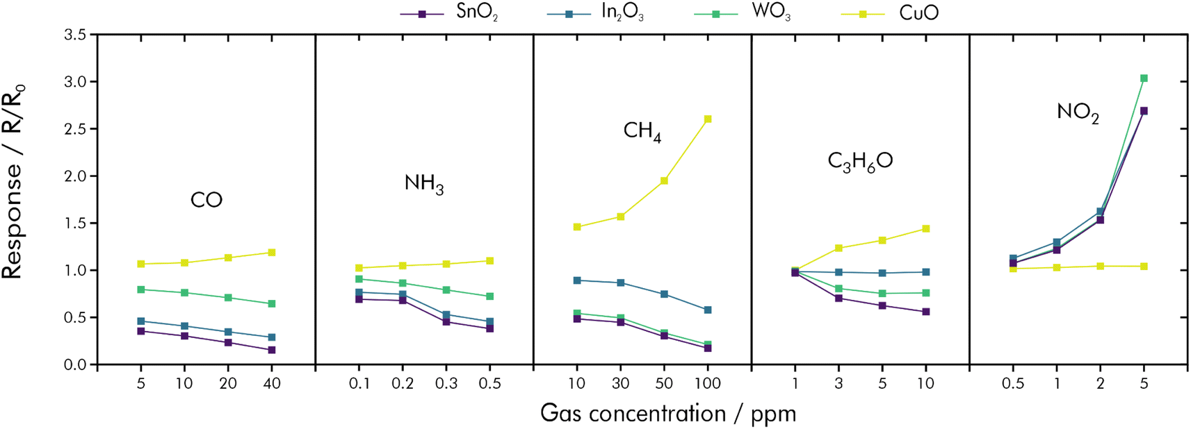 | ||
| Fig. 15 Signal responses and sample variations of SnO2, In2O3, WO3 and CuO towards CO, NH3, CH4, acetone and NO2; reprinted (adapted) with permission from ref. 162. Copyright 2022 American Chemical Society. | ||
The power of statistical analysis was recently further demonstrated by a comparable method successfully simulating and determining the concentration of NOx in synthetic air under changing humidity and temperature. Here an artificial neural network was fed time dependent signal responses of four sensor substrates of the same material, but with different layer thicknesses.163 It is expected that such data analysis protocols will be beneficial for all kinds of chemiresistive gas sensors.
In an approach, which was proposed by Hasan et al., various sensing parameters, such as signal response, response- and recovery time and several fitting parameters are extracted from time-resolved measurements of NO2, NH3, RH and mixtures thereof on a rGO/CuCoOx sensor.164 A total of ten parameters, as shown in Fig. 16 is then fed through PCA and machine intelligent recognition and regression to classify each target gas and determine its concentration. Classification was tested by seven different algorithms (decision tree, linear discriminant, naïve bayes, support vector machine, k-nearest neighbor, ensemble bagged trees, and a neural network) most of which reached a high accuracy. K-nearest neighbor (kNN) was chosen by the authors for its advantage that no prior assumptions are necessary. KNN was able to classify the used mixtures with an accuracy of 98% within the validation set and quantify in an error range of 10%. The type of measurement required to obtain the necessary data, however, rules out the possibility of continuous monitoring.164
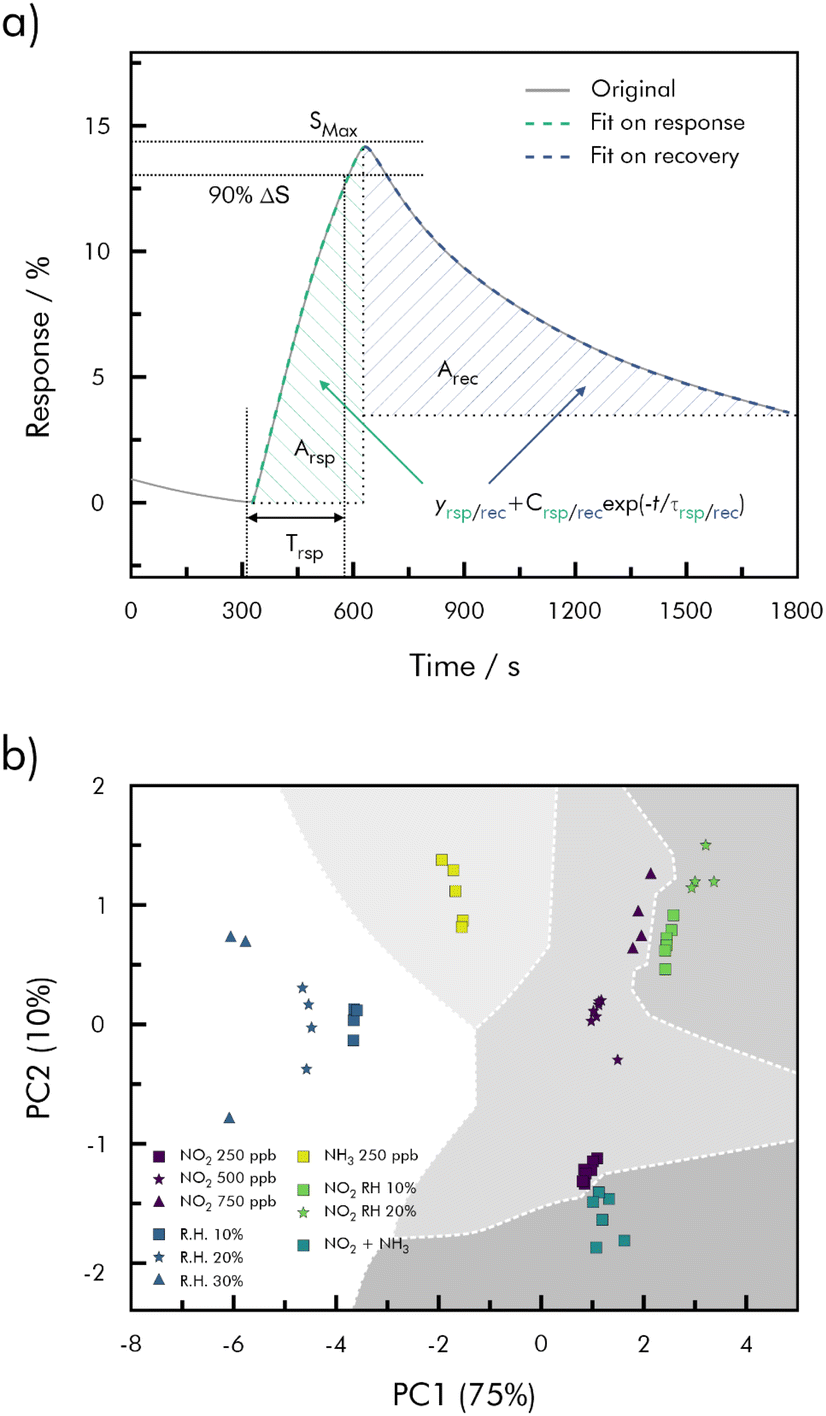 | ||
| Fig. 16 (a) Feature extraction from the gas response curve (red and blue lines are the exponential fitted curves for the response and recovery regime); (b) decision map for NO2, humid air, NH3, NO2 under humid air, and a mixture of NO2 and NH3 classified by applying k-nearest neighbor (kNN) to the PCA model with k = 5; redrawn and adapted from ref. 164. | ||
The data acquisition and computing processes are sometimes complex and bear the risk of high energy consumption. For IoT applications this can quickly become an issue and along with sensors, also sensing circuits with low power demands need to be developed. Such a low-power integrated circuit for reading the responses of a simple PANI-based NH3 sensor as well as a pristine graphene NO2 sensor was shown to be able to interface with a resistance range from 1 kΩ to 33 MΩ and generate bias voltages from 50 mV to 1 V.165
Conclusion
In this review general mechanisms in chemiresistive gas sensing using graphene-based receptors are discussed regarding sensitivity, reversibility, LOD and especially selectivity. Graphene and its derivatives are shown here to be highly useful materials with exceptional sensing capabilities even at room temperature and allow the tuning of their electrical characteristics like conductance or bandgap by controlling the number of lattice defects, doping or temperature.Chemiresistive sensors made exclusively from graphene, however, suffer from low selectivity and are highly susceptible to humidity, when operated under ambient conditions. Combining graphene with other semiconducting materials, such as MOx, TMDs, or polymers was shown to improve the sensing characteristics towards selectivity through synergistic effects. Yet, true selectivity with a high sensitivity especially under ambient conditions is still very difficult to achieve and more often seems like a fortunate coincidence. As long as the intricate mechanisms and reasons for certain, seemingly specific, interactions between a sensor and target gas are (in most cases) not fully understood, truly targeted material development is a big challenge. In a related field of graphene-research this problem has been reviewed already and is applicable here just as well.166
Tackling the issue of humidity, several strategies have been proposed. They include such simple, but counterproductive solutions, like operating at elevated temperatures, which conflicts the urge to minimize power consumption. Other approaches are more promising, like surface coatings with water-impermeable membranes, or MIPs. These may however increase response and recovery-times, due to slower diffusion of analyte gases to the sensitive layer. Finally, considering humidity as an interfering gas, improving the selectivity through advanced measurement and readout techniques may hold the key.
A way to approach the general problem of selectivity is offered by readout techniques that are capable of processing complex and multiparametric data. Rather than relying, e.g., on a single sensor, that is selective and sensitive, but often badly reversible towards one or a few target gases, arrays of multiple semi-selective receptors have been proposed. These electronic noses provide several independent signals, which can be fed trough pattern-recognition algorithms to obtain information about the state of the monitored system. As a way to tackle selectivity and reversibility of chemiresistive gas sensors simultaneously, it was shown that applying AC instead of commonly used DC voltages, influences the binding strength and response of gas molecules to the sensor surface and facilitates desorption processes. Furthermore, signal responses are dependent on the frequency of the applied voltage. This may transfer from the signal strength for a single target gas to a frequency dependent signal patten for several gases in a mixture, which again can possibly be evaluated by intelligent algorithms. Alternatively, different gases and mixtures can be classified by interpretation of kinetic measurement parameters through machine learning and quantified by regression-, or principal component regression algorithms, however, not as easily for continuous monitoring applications.
Standard setups and simple sensor devices can therefore be operated to deliver sensitive and selective signal responses by the assistance of artificial intelligence. Their application is not limited to a single data processing- or a single classification algorithm, but it may profit from the combined effort of several. Nevertheless, one must keep in mind, that complex computing operations also can take a high toll on the total power demand to a sensor system and may at some point outweigh the energy savings from low operating temperatures.
Further, the long-term stability of such devices is not sufficiently addressed in current research and stability tests often only span several days or weeks and a rather low number of measurement cycles. Therefore, introducing chemiresistive gas sensors to mass production and serial application, still requires research to ensure long lifetimes even under harsh conditions.
Mass production of graphene-based sensors, however, also requires a reliable coating or deposition process, which is responsible for large variations between devices in a series. High quality coatings obtained by current methods either rely on complicated transfer techniques, e.g., from vapor deposited materials, or lack uniformity, e.g., through drop-deposition. Much work has therefore been put into the development of alternative processes, that include electrochemical, or electrophoretic deposition,167–169 as well as covalent bonds between graphene and a surface function,170 some of which are still to be tested for their applicability in gas sensors.
While graphene has also proven to be a suitable sensing material for flexible sensors, the greater challenges in this of application area arise from the flexibility of the carrier electronics. Since most substrates hardly bend in the μm range, sufficient miniaturization of the transducer element is equally effective for the operation of such devices. Therefore, graphene-based sensors designed for flexible, or wearable devices have not been specifically addressed in this review.
Conflicts of interest
There are no conflicts to declare.Notes and references
- E. Cheek, V. Guercio, C. Shrubsole and S. Dimitroulopoulou, Sci. Total Environ., 2020, 766, 142585, DOI:10.1016/j.scitotenv.2020.142585.
- C. E. Dujardin, R. A. T. Mars, S. M. Manemann, P. C. Kashyap, N. S. Clements, L. C. Hassett and V. L. Roger, Environ. Res., 2020, 186, 109485, DOI:10.1016/j.envres.2020.109485.
- J. Saini, M. Dutta and G. Marques, Sustainable Environ. Res., 2020, 30, 6, DOI:10.1186/s42834-020-0047-y.
- P. Wolkoff, Int. J. Hyg. Environ. Health, 2018, 221, 376–390, DOI:10.1016/j.ijheh.2018.01.015.
- H. Boogaard, A. M. van Erp, K. D. Walker and R. Shaikh, Curr. Environ. Health Rep., 2017, 4, 514–522, DOI:10.1007/s40572-017-0161-0.
- P. J. M. Koken, W. T. Piver, F. Ye, A. Elixhauser, L. M. Olsen and C. J. Portier, Environ. Health Perspect., 2003, 111, 1312–1317, DOI:10.1289/ehp.5957.
- J.-B. Ruidavets, M. Cournot, S. Cassadou, M. Giroux, M. Meybeck and J. Ferrières, Circulation, 2005, 111, 563–569, DOI:10.1161/01.cir.0000154546.32135.6e.
- World Health Organization, WHO Global Air Quality Guidelines: Particulate Matter (PM2.5 and PM10), Ozone, Nitrogen dioxide, Sulfur Dioxide and Carbon Monoxide, https://apps.who.int/iris/handle/10665/345329, accessed 17 March 2023 Search PubMed.
- S. Costa, J. Ferreira, C. Silveira, C. Costa, D. Lopes, H. Relvas, C. Borrego, P. Roebeling, A. I. Miranda and J. P. Teixeira, J. Toxicol. Environ. Health, Part B, 2014, 17, 307–340, DOI:10.1080/10937404.2014.946164.
- Directive 2008/50/EC of the European Parliament and of the Council of 21 May 2008 on Ambient Air Quality and Cleaner Air for Europe, http://data.europa.eu/eli/dir/2008/50/2015-09-18, accessed 17 March 2023 Search PubMed.
- German Research Foundation, List of MAK and BAT Values 2022, https://series.publisso.de/en/pgseries/overview/mak/lmbv/curIssue, accessed 17 March 2023 Search PubMed.
- S. Dhall, B. R. Mehta, A. K. Tyagi and K. Sood, Sens. Int., 2021, 2, 100116, DOI:10.1016/j.sintl.2021.100116.
- J. B. A. Gomes, J. J. P. C. Rodrigues, R. A. L. Rabêlo, N. Kumar and S. Kozlov, J. Sens. Actuator Netw., 2019, 8, 57, DOI:10.3390/jsan8040057.
- D. J. Kearney, T. Hubbard and D. Putnam, Dig. Dis. Sci., 2002, 47, 2523–2530, DOI:10.1023/A:1020568227868.
- B. V. Krsihna, S. Ravi and M. D. Prakash, Mater. Today: Proc., 2021, 45, 1524–1528, DOI:10.1016/j.matpr.2020.07.678.
- S. Yang, C. Jiang and S. Wei, Appl. Phys. Rev., 2017, 4, 21304, DOI:10.1063/1.4983310.
- M. Mayer and A. J. Baeumner, Chem. Rev., 2019, 119, 7996–8027, DOI:10.1021/acs.chemrev.8b00719.
- B. Liu, L. Chen, G. Liu, A. N. Abbas, M. Fathi and C. Zhou, ACS Nano, 2014, 8, 5304–5314, DOI:10.1021/nn5015215.
- N. Joshi, T. Hayasaka, Y. Liu, H. Liu, O. N. Oliveira and L. Lin, Mikrochim. Acta, 2018, 185, 213, DOI:10.1007/s00604-018-2750-5.
- S.-J. Choi and I.-D. Kim, Electron. Mater. Lett., 2018, 14, 221–260, DOI:10.1007/s13391-018-0044-z.
- C. Kittel, Introduction to Solid State Physics, John Wiley & Sons, 8th edn, 2005 Search PubMed.
- F. Schedin, A. K. Geim, S. V. Morozov, E. W. Hill, P. Blake, M. I. Katsnelson and K. S. Novoselov, Nat. Mater., 2007, 6, 652–655, DOI:10.1038/nmat1967.
- S. S. Varghese, S. Lonkar, K. K. Singh, S. Swaminathan and A. Abdala, Sens. Actuators, B, 2015, 218, 160–183, DOI:10.1016/j.snb.2015.04.062.
- Y. Xu, C. Cheng, S. Du, J. Yang, B. Yu, J. Luo, W. Yin, E. Li, S. Dong, P. Ye and X. Duan, ACS Nano, 2016, 10, 4895–4919, DOI:10.1021/acsnano.6b01842.
- L. Zhang, K. Khan, J. Zou, H. Zhang and Y. Li, Adv. Mater. Interfaces, 2019, 6, 1901329, DOI:10.1002/admi.201901329.
- X. Li and H. Zhu, Phys. Today, 2016, 69, 46–51, DOI:10.1063/pt.3.3298.
- A. Javey and J. Kong, Carbon Nanotube Electronics, Spinger Science+Business Media, New York, USA, 2009 Search PubMed.
- X. Cui, M. Freitag, R. Martel, L. Brus and P. Avouris, Nano Lett., 2003, 3, 783–787, DOI:10.1021/nl034193a.
- J. Nah, S. B. Kumar, H. Fang, Y.-Z. Chen, E. Plis, Y.-L. Chueh, S. Krishna, J. Guo and A. Javey, J. Phys. Chem. C, 2012, 116, 9750–9754, DOI:10.1021/jp300446z.
- A. Javey, J. Guo, Q. Wang, M. Lundstrom and H. Dai, Nature, 2003, 424, 654–657, DOI:10.1038/nature01797.
- Y. Kim, S.-K. Kang, N.-C. Oh, H.-D. Lee, S.-M. Lee, J. Park and H. Kim, ACS Appl. Mater. Interfaces, 2019, 11, 38902–38909, DOI:10.1021/acsami.9b10861.s001.
- G. Giovanetti, P. A. Khomyakov, G. Brocks, V. M. Karpan, J. van den Brink and P. J. Kelly, Phys. Rev. Lett., 2008, 101, 26803, DOI:10.1103/PhysRevLett.101.026803.
- S. Heo, E. Cho, H.-I. Lee, G. S. Park, H. J. Kang, T. Nagatomi, P. Choi and B.-D. Choi, AIP Adv., 2015, 5, 77167, DOI:10.1063/1.4927547.
- D. G. Larrude, Y. Garcia-Basabe, F. L. Freire Junior and M. L. M. Rocco, RSC Adv., 2015, 5, 74189–74197, 10.1039/c5ra12799h.
- M. Sprinkle, D. Siegel, Y. Hu, J. Hicks, A. Tejeda, A. Taleb-Ibrahimi, P. Le Fèvre, F. Bertran, S. Vizzini, H. Enriquez, S. Chiang, P. Soukiassian, C. Berger, W. A. de Heer, A. Lanzara and E. H. Conrad, Phys. Rev. Lett., 2009, 103, 226803, DOI:10.1103/PhysRevLett.103.226803.
- M. Batzill, Surf. Sci. Rep., 2012, 67, 83–115, DOI:10.1016/j.surfrep.2011.12.001.
- S. W. Han, H. Kwon, S. K. Kim, S. Ryu, W. S. Yun, D. H. Kim, J. H. Hwang, J.-S. Kang, J. Baik, H. J. Shin and S. C. Hong, Phys. Rev. B, 2011, 84, 45409, DOI:10.1103/PhysRevB.84.045409.
- S. Naghdi, G. Sanchez-Arriaga and K. Y. Rhee, J. Alloys Compd., 2019, 805, 1117–1134, DOI:10.1016/j.jallcom.2019.07.187.
- A. Grillo and A. Di Bartolomeo, Adv. Electron. Mater., 2021, 7, 2000979, DOI:10.1002/aelm.202000979.
- S. Y. Park, Y. H. Kim, S. Y. Lee, W. Sohn, J. E. Lee, D. H. Kim, Y.-S. Shim, K. C. Kwon, K. S. Choi, H. J. Yoo, J. M. Suh, M. Ko, J.-H. Lee, M. J. Lee, S. Y. Kim, M. H. Lee and H. W. Jang, J. Mater. Chem. A, 2018, 6, 5016–5024, 10.1039/c7ta11375g.
- A. W. Cummings, D. L. Duong, L. van Nguyen, D. van Tuan, J. Kotakoski, J. E. Barrios Vargas, Y. H. Lee and S. Roche, Adv. Mater., 2014, 26, 5079–5094, DOI:10.1002/adma.201401389.
- A. Afzal, N. Cioffi, L. Sabbatini and L. Torsi, Sens. Actuators, B, 2012, 171–172, 25–42, DOI:10.1016/j.snb.2012.05.026.
- W.-T. Koo, H.-J. Cho, D.-H. Kim, Y. H. Kim, H. Shin, R. M. Penner and I.-D. Kim, ACS Nano, 2020, 14, 14284–14322, DOI:10.1021/acsnano.0c05307.
- K. Khun Khun, A. Mahajan and R. K. Bedi, J. Appl. Phys., 2009, 106, 124509, DOI:10.1063/1.3273323.
- R. Ghosh, S. Santra, S. K. Ray and P. K. Guha, Appl. Phys. Lett., 2015, 107, 153102, DOI:10.1063/1.4933110.
- J. Zhu, M. Cho, Y. Li, I. Cho, J.-H. Suh, D. Del Orbe, Y. Jeong, T.-L. Ren and I. Park, ACS Appl. Mater. Interfaces, 2019, 11, 24386–24394, DOI:10.1021/acsami.9b04495.
- I. Karaduman, E. Er, H. Çelikkan, N. Erk and S. Acar, J. Alloys Compd., 2017, 722, 569–578, DOI:10.1016/j.jallcom.2017.06.152.
- N. Barsan and U. Weimar, J. Electroceram., 2001, 7, 143–167, DOI:10.1023/A:1014405811371.
- J. Zhang, S. Wang, Y. Wang, Y. Wang, B. Zhu, H. Xia, X. Guo, S. Zhang, W. Huang and S. Wu, Sens. Actuators, B, 2009, 135, 610–617, DOI:10.1016/j.snb.2008.09.026.
- S.-J. Kim, I.-S. Hwang, J.-K. Choi and J.-H. Lee, Thin Solid Films, 2011, 519, 2020–2024, DOI:10.1016/j.tsf.2010.10.026.
- X. Gou, R. Li, G. Wang, Z. Chen and D. Wexler, Nanotechnology, 2009, 20, 495501, DOI:10.1088/0957-4484/20/49/495501.
- P.-S. Cho, K.-W. Kim and J.-H. Lee, J. Electroceram., 2006, 17, 975–978, DOI:10.1007/s10832-006-8146-7.
- J. Gao, H. Wu, J. Zhou, L. Yao, G. Zhang, S. Xu, Y. Xie, L. Li and K. Shi, New J. Chem., 2016, 40, 1306–1311, 10.1039/c5nj02214b.
- Z. Li, N. Wang, Z. Lin, J. Wang, W. Liu, K. Sun, Y. Q. Fu and Z. Wang, ACS Appl. Mater. Interfaces, 2016, 8, 20962–20968, DOI:10.1021/acsami.6b02893.
- J. Wang, L. Wei, L. Zhang, C. Jiang, E. Siu-Wai Kong and Y. Zhang, J. Mater. Chem., 2012, 22, 8327, 10.1039/c2jm16934g.
- O. Lupan, V. Postica, N. Wolff, O. Polonskyi, V. Duppel, V. Kaidas, E. Lazari, N. Ababii, F. Faupel, L. Kienle and R. Adelung, Localized Synthesis of Iron Oxide Nanowires and Fabrication of High Performance Nanosensors Based on a Single Fe2O3 Nanowire, Small, 2017, 13, 1602868, DOI:10.1002/smll.201602868.
- C. Matei Ghimbeu, M. Lumbreras, M. Siadat and J. Schoonman, Mater. Sci. Semicond. Process., 2010, 13, 1–8, DOI:10.1016/j.mssp.2010.01.001.
- H. Hashtroudi, I. D. R. Mackinnon and M. Shafiei, J. Mater. Chem. C, 2020, 8, 13108–13126, 10.1039/d0tc01968b.
- R. Kumar, N. Goel, M. Hojamberdiev and M. Kumar, Sens. Actuators, A, 2020, 303, 111875, DOI:10.1016/j.sna.2020.111875.
- G. Lu, L. E. Ocola and J. Chen, Nanotechnology, 2009, 20, 445502, DOI:10.1088/0957-4484/20/44/445502.
- A. Reina, X. Jia, J. Ho, D. Nezich, H. Son, V. Bulovic, M. S. Dresselhaus and J. Kong, Nano Lett., 2009, 9, 30–35, DOI:10.1021/nl801827v.
- T. Zhang, J. Liu, C. Wang, X. Leng, Y. Xiao and L. Fu, Biosens. Bioelectron., 2017, 89, 28–42, DOI:10.1016/j.bios.2016.06.072.
- N. Kumar, R. Salehiyan, V. Chauke, O. Joseph Botlhoko, K. Setshedi, M. Scriba, M. Masukume and S. S. Ray, FlatChem, 2021, 27, 100224, DOI:10.1016/j.flatc.2021.100224.
- G. Chen, T. M. Paronyan and A. R. Harutyunyan, Appl. Phys. Lett., 2012, 101, 53119, DOI:10.1063/1.4742327.
- S. Basu and P. Bhattacharyya, Sens. Actuators, B, 2012, 173, 1–21, DOI:10.1016/j.snb.2012.07.092.
- S. Bae, H. Kim, Y. Lee, X. Xu, J.-S. Park, Y. Zheng, J. Balakrishnan, T. Lei, H. R. Kim, Y. I. Song, Y.-J. Kim, K. S. Kim, B. Özyilmaz, J.-H. Ahn, B. H. Hong and S. Iijima, Nat. Nanotechnol., 2010, 5, 574–578, DOI:10.1038/nnano.2010.132.
- W. S. Hummers and R. E. Offeman, J. Am. Chem. Soc., 1958, 80, 1339, DOI:10.1021/ja01539a017.
- I. Jung, D. A. Dikin, R. D. Piner and R. S. Ruoff, Nano Lett., 2008, 8, 4283–4287, DOI:10.1021/nl8019938.
- R. S. Edwards and K. S. Coleman, Nanoscale, 2013, 5, 38–51, 10.1039/c2nr32629a.
- S. Eigler, M. Enzelberger-Heim, S. Grimm, P. Hofmann, W. Kroener, A. Geworski, C. Dotzer, M. Röckert, J. Xiao, C. Papp, O. Lytken, H.-P. Steinrück, P. Müller and A. Hirsch, Adv. Mater., 2013, 25, 3583–3587, DOI:10.1002/adma.201300155.
- J. Park, Y. Kim, S. Y. Park, S. J. Sung, H. W. Jang and C. R. Park, Carbon, 2020, 159, 175–184, DOI:10.1016/j.carbon.2019.11.063.
- V. Rodríguez-Lugo, D. Sánchez-Campos, D. Mendoza-Anaya, M. I. Reyes Valderrama, L. Escobar-Alarcón, E. Salinas-Rodríguez and T. V. K. Karthik, Appl. Phys. A, 2021, 127, 533, DOI:10.1007/s00339-021-04665-9.
- S. Eigler, C. Dotzer and A. Hirsch, Carbon, 2012, 50, 3666–3673, DOI:10.1016/j.carbon.2012.03.039.
- K. Kim, H. J. Park, B.-C. Woo, K. J. Kim, G. T. Kim and W. S. Yun, Nano Lett., 2008, 8, 3092–3096, DOI:10.1021/nl8010337.
- L. G. Cançado, A. Jorio, E. H. Martins Ferreira, F. Stavale, C. A. Achete, R. B. Capaz, M. V. O. Moutinho, A. Lombardo, T. S. Kulmala and A. C. Ferrari, Nano Lett., 2011, 11, 3190–3196, DOI:10.1021/nl201432g.
- A. Zöpfl, M.-M. Lemberger, M. König, G. Ruhl, F.-M. Matysik and T. Hirsch, Faraday Discuss., 2014, 173, 403–414, 10.1039/c4fd00086b.
- M. J. Fernández-Merino, L. Guardia, J. I. Paredes, S. Villar-Rodil, P. Solís-Fernández, A. Martínez-Alonso and J. M. D. Tascón, J. Phys. Chem. C, 2010, 114, 6426–6432, DOI:10.1021/jp100603h.
- H.-J. Shin, K. K. Kim, A. Benayad, S.-M. Yoon, H. K. Park, I.-S. Jung, M. H. Jin, H.-K. Jeong, J. M. Kim, J.-Y. Choi and Y. H. Lee, Adv. Funct. Mater., 2009, 19, 1987–1992, DOI:10.1002/adfm.200900167.
- S. Y. Toh, K. S. Loh, S. K. Kamarudin and W. R. W. Daud, Chem. Eng. J., 2014, 251, 422–434, DOI:10.1016/j.cej.2014.04.004.
- H. A. Becerril, J. Mao, Z. Liu, R. M. Stoltenberg, Z. Bao and Y. Chen, ACS Nano, 2008, 2, 463–470, DOI:10.1021/nn700375n.
- S. Grimm, M. Schweiger, S. Eigler and J. Zaumseil, J. Phys. Chem. C, 2016, 120, 3036–3041, DOI:10.1021/acs.jpcc.5b11598.
- H. Hashtroudi, R. Kumar, R. Savu, S. Moshkalev, G. Kawamura, A. Matsuda and M. Shafiei, Int. J. Hydrogen Energy, 2021, 46, 7653–7665, DOI:10.1016/j.ijhydene.2020.11.268.
- H. Huang, Z. Li, J. She and W. Wang, J. Appl. Phys., 2012, 111, 54317, DOI:10.1063/1.3694665.
- P. V. Kumar, M. Bernardi and J. C. Grossman, ACS Nano, 2013, 7, 1638–1645, DOI:10.1021/nn305507p.
- P. Feicht and S. Eigler, ChemNanoMat, 2018, 4, 244–252, DOI:10.1002/cnma.201700357.
- G. Capote Mastrapa and F. L. Freire Junior, J. Sens., 2019, 2019, 1–7, DOI:10.1155/2019/5492583.
- R. Kumar, D. K. Avasthi and A. Kaur, Sens. Actuators, B, 2017, 242, 461–468, DOI:10.1016/j.snb.2016.11.018.
- J. Wu, Z. Li, X. Xie, K. Tao, C. Liu, K. A. Khor, J. Miao and L. K. Norford, J. Mater. Chem. A, 2018, 6, 478–488, 10.1039/c7ta08775f.
- W. Li, X. Li, L. Cai, Y. Sun, M. Sun and D. Xie, J. Nanosci. Nanotechnol., 2018, 18, 7927–7932, DOI:10.1166/jnn.2018.15563.
- Y.-J. Choi, I.-S. Hwang, J.-G. Park, K. J. Choi, J.-H. Park and J.-H. Lee, Nanotechnology, 2008, 19, 95508, DOI:10.1088/0957-4484/19/9/095508.
- C.-Y. Lin, Y.-Y. Fang, C.-W. Lin, J. J. Tunney and K.-C. Ho, Sens. Actuators, B, 2010, 146, 28–34, DOI:10.1016/j.snb.2010.02.040.
- K. Lee, R. Gatensby, N. McEvoy, T. Hallam and G. S. Duesberg, Adv. Mater., 2013, 25, 6699–6702, DOI:10.1002/adma.201303230.
- J. Li, Y. Lu, Q. Ye, M. Cinke, J. Han and M. Meyyappan, Nano Lett., 2003, 3, 929–933, DOI:10.1021/nl034220x.
- L. Kumar, I. Rawal, A. Kaur and S. Annapoorni, Sens. Actuators, B, 2017, 240, 408–416, DOI:10.1016/j.snb.2016.08.173.
- H.-H. Lu, C.-Y. Lin, T.-C. Hsiao, Y.-Y. Fange, K.-C. Ho, D. Yang, C.-K. Lee, S.-M. Hsu and C.-W. Lin, Anal. Chim. Acta, 2009, 640, 68–74, DOI:10.1016/j.aca.2009.03.006.
- G. Korotcenkov and B. K. Cho, Sens. Actuators, B, 2017, 244, 182–210, DOI:10.1016/j.snb.2016.12.117.
- T. Zhang, S. Mubeen, N. V. Myung and M. A. Deshusses, Nanotechnology, 2008, 19, 332001, DOI:10.1088/0957-4484/19/33/332001.
- Y. C. Wong, B. C. Ang, A. S. M. A. Haseeb and A. A. Baharuddin, J. Electrochem. Soc., 2020, 167, 37503, DOI:10.1149/2.0032003JES.
- T. Kuila, S. Bose, A. K. Mishra, P. Khanra, N. H. Kim and J. H. Lee, Prog. Mater. Sci., 2012, 57, 1061–1105, DOI:10.1016/j.pmatsci.2012.03.002.
- T. Wei, O. Martin, S. Yang, F. Hauke and A. Hirsch, Angew. Chem., Int. Ed., 2019, 58, 816–820, DOI:10.1002/anie.201811864.
- K. Jayaramulu, M. Esclance DMello, K. Kesavan, A. Schneemann, M. Otyepka, S. Kment, C. Narayana, S. B. Kalidindi, R. S. Varma, R. Zboril and R. A. Fischer, J. Mater. Chem. A, 2021, 9, 17434–17441, 10.1039/D1TA03246A.
- S. F. Liu, L. C. H. Moh and T. M. Swager, Chem. Mater., 2015, 27, 3560–3563, DOI:10.1021/acs.chemmater.5b00153.
- Y. Huang, W. Jiao, Z. Chu, G. Ding, M. Yan, X. Zhong and R. Wang, J. Mater. Chem. C, 2019, 7, 8616–8625, 10.1039/c9tc02436k.
- A. Hermawan, N. L. W. Septiani, A. Taufik, B. Yuliarto, Suyatman and S. Yin, Nano-Micro Lett., 2021, 13, 207, DOI:10.1007/s40820-021-00724-1.
- H. Liu, Y. Liu and D. Zhu, J. Mater. Chem., 2011, 21, 3335–3345, 10.1039/c0jm02922j.
- V. Georgakilas, M. Otyepka, A. B. Bourlinos, V. Chandra, N. Kim, K. C. Kemp, P. Hobza, R. Zboril and K. S. Kim, Chem. Rev., 2012, 112, 6156–6214, DOI:10.1021/cr3000412.
- Z. J. Guo, B. Wang, X. Wang, Y. Li, S. Gai, Y. Wu and X. L. Cheng, RSC Adv., 2019, 9, 37518–37525, 10.1039/c9ra08065a.
- H. Song, X. Li, P. Cui, S. Guo, W. Liu and X. Wang, Sens. Actuators, B, 2017, 244, 124–130, DOI:10.1016/j.snb.2016.12.133.
- E. Lee, J. M. Lee, J. H. Koo, W. Lee and T. Lee, Int. J. Hydrogen Energy, 2010, 35, 6984–6991, DOI:10.1016/j.ijhydene.2010.04.051.
- A. V. Singhal, H. Charaya and I. Lahiri, Crit. Rev. Solid State Mater. Sci., 2017, 42, 499–526, DOI:10.1080/10408436.2016.1244656.
- D. H. Shin, J. S. Lee, J. Jun, J. H. An, S. G. Kim, K. H. Cho and J. Jang, Sci. Rep., 2015, 5, 12294, DOI:10.1038/srep12294.
- D.-T. Phan and G.-S. Chung, Int. J. Hydrogen Energy, 2014, 39, 20294–20304, DOI:10.1016/j.ijhydene.2014.10.006.
- J. Hong, S. Lee, J. Seo, S. Pyo, J. Kim and T. Lee, ACS Appl. Mater. Interfaces, 2015, 7, 3554–3561, DOI:10.1021/am5073645.
- Y. Kim, Y. S. Choi, S. Y. Park, T. Kim, S.-P. Hong, T. H. Lee, C. W. Moon, J.-H. Lee, D. Lee, B. H. Hong and H. W. Jang, Nanoscale, 2019, 11, 2966–2973, 10.1039/c8nr09076a.
- I. Fratoddi, I. Venditti, C. Cametti and M. V. Russo, Sens. Actuators, B, 2015, 220, 534–548, DOI:10.1016/j.snb.2015.05.107.
- M. R. U. D. Biswas and W.-C. Oh, RSC Adv., 2019, 9, 11484–11492, 10.1039/c9ra00007k.
- V. Georgakilas, M. Otyepka, A. B. Bourlinos, V. Chandra, N. Kim, K. C. Kemp, P. Hobza, R. Zboril and K. S. Kim, Chem. Rev., 2012, 112, 5553–6214, DOI:10.1021/cr3000412.
- German Environment Agency, Air-Quality Measurement Stations, https://www.umweltbundesamt.de/en/data/air/air-data/stations, accessed 16 March 2023 Search PubMed.
- Deutscher Wetterdienst, Zahlen und Fakten zum Deutschen Wetterdienst 2023, https://www.dwd.de/SharedDocs/downloads/DE/allgemein/zahlen_und_fakten.html, accessed 17 March 2023 Search PubMed.
- R. J. Francey, C. M. Trudinger, M. van der Schoot, R. M. Law, P. B. Krummel, R. L. Langenfelds, L. Paul Steele, C. E. Allison, A. R. Stavert, R. J. Andres and C. Rödenbeck, Nat. Clim. Change, 2013, 3, 520–524, DOI:10.1038/nclimate1817.
- National Aeronautics and Space Administration (NASA), Earth Fact Sheet, https://nssdc.gsfc.nasa.gov/planetary/factsheet/earthfact.html, accessed 17 March 2023 Search PubMed.
- S. Grice, J. Stedman, A. Kent, M. Hobson, J. Norris, J. Abbott and S. Cooke, Atmos. Environ., 2009, 43, 2154–2167, DOI:10.1016/j.atmosenv.2009.01.019.
- D. Schwela, Rev. Environ. Health, 2000, 15, 13–42, DOI:10.1515/reveh.2000.15.1-2.13.
- I. Mavroidis and M. Ilia, Atmos. Environ., 2012, 63, 135–147, DOI:10.1016/j.atmosenv.2012.09.030.
- J. Cyrys, M. Eeftens, J. Heinrich, C. Ampe, A. Armengaud, R. Beelen, T. Bellander, T. Beregszaszi, M. Birk, G. Cesaroni, M. Cirach, K. de Hoogh, A. de Nazelle, F. de Vocht, C. Declercq, A. Dėdelė, K. Dimakopoulou, K. Eriksen, C. Galassi, R. Grąulevičienė, G. Grivas, O. Gruzieva, A. H. Gustafsson, B. Hoffmann, M. Iakovides, A. Ineichen, U. Krämer, T. Lanki, P. Lozano, C. Madsen, K. Meliefste, L. Modig, A. Mölter, G. Mosler, M. Nieuwenhuijsen, M. Nonnemacher, M. Oldenwening, A. Peters, S. Pontet, N. Probst-Hensch, U. Quass, O. Raaschou-Nielsen, A. Ranzi, D. Sugiri, E. G. Stephanou, P. Taimisto, M.-Y. Tsai, É. Vaskövi, S. Villani, M. Wang, B. Brunekreef and G. Hoek, Atmos. Environ., 2012, 62, 374–390, DOI:10.1016/j.atmosenv.2012.07.080.
- United States Environmental Protection Agency (EPA), Nitrogen Dioxide (NO2) Pollution, http://www.epa.gov/no2-pollution, accessed 17 March 2023 Search PubMed.
- U. S. EPA, OAQPS and CATC, Nitrogen Oxides (NOx) Why and How They Are Controlled, 1999 Search PubMed.
- J. Brunet, M. Dubois, A. Pauly, L. Spinelle, A. Ndiaye, K. Guérin, C. Varenne and B. Lauron, Sens. Actuators, B, 2012, 173, 659–667, DOI:10.1016/j.snb.2012.07.082.
- Y.-S. Chang, F.-K. Chen, D.-C. Tsai, B.-H. Kuo and F.-S. Shieu, Sci. Rep., 2021, 11, 20719, DOI:10.1038/s41598-021-99883-9.
- D.-B. Moon, A. Bag, H.-B. Lee, M. Meeseepong, D.-H. Lee and N.-E. Lee, Sens. Actuators, B, 2021, 345, 130373, DOI:10.1016/j.snb.2021.130373.
- L. Yang, G. Zheng, Y. Cao, C. Meng, Y. Li, H. Ji, X. Chen, G. Niu, J. Yan, Y. Xue and H. Cheng, Microsyst. Nanoeng., 2022, 8, 78, DOI:10.1038/s41378-022-00414-x.
- Y. Gao, J. Wang, Y. Feng, N. Cao, H. Li, N. F. de Rooij, A. Umar, P. J. French, Y. Wang and G. Zhou, Small, 2022, 18, 2103259, DOI:10.1002/smll.202103259.
- R. Ghanbari, R. Safaiee, M. H. Sheikhi, M. M. Golshan and Z. K. Horastani, ACS Appl. Mater. Interfaces, 2019, 11, 21795–21806, DOI:10.1021/acsami.9b00625.
- J. E. Ellis, D. C. Sorescu, S. I. Hwang, S. C. Burkert, D. L. White, H. Kim and A. Star, ACS Appl. Mater. Interfaces, 2019, 11, 41588–41594, DOI:10.1021/acsami.9b13440.
- M. Son, Y. Pak, S.-S. Chee, F. M. Auxilia, K. Kim, B.-K. Lee, S. Lee, S. K. Kang, C. Lee, J. S. Lee, K. K. Kim, Y. H. Jang, B. H. Lee, G.-Y. Jung and M.-H. Ham, Nano Res., 2018, 11, 3529–3536, DOI:10.1007/s12274-017-1857-z.
- Schweizerische Unfallversicherungsanstalt (suva), Aktuelle MAK und BAT Werte, https://www.suva.ch/de-CH/material/Richtlinien-Gesetzestexte/grenzwerte-am-arbeitsplatz-aktuelle-werte#gnw-location=%2F, accessed 17 March 2023 Search PubMed.
- K. L. Cashdollar, I. A. Zlochower, G. M. Green, R. A. Thomas and M. Hertzberg, J. Loss Prev. Process Ind., 2000, 13, 327–340, DOI:10.1016/S0950-4230(99)00037-6.
- A. Giampiccolo, D. M. Tobaldi, S. G. Leonardi, B. J. Murdoch, M. P. Seabra, M. P. Ansell, G. Neri and R. J. Ball, Appl. Catal., B, 2019, 243, 183–194, DOI:10.1016/j.apcatb.2018.10.032.
- H. Bai, H. Guo, C. Feng, J. Wang, B. Liu, Z. Xie, F. Guo, D. Chen, R. Zhang and Y. Zheng, J. Mater. Chem. C, 2022, 10, 3756–3769, 10.1039/d1tc05231d.
- J. Moon, Y. Cheng, L. L. Daemen, M. Li, F. Polo-Garzon, A. J. Ramirez-Cuesta and Z. Wu, ACS Catal., 2020, 10, 5278–5287, DOI:10.1021/acscatal.0c00808.
- A. Esfandiar, A. Irajizad, O. Akhavan, S. Ghasemi and M. R. Gholami, Int. J. Hydrogen Energy, 2014, 39, 8169–8179, DOI:10.1016/j.ijhydene.2014.03.117.
- A. Kapoor, J. A. Ritter and R. T. Yang, Langmuir, 1990, 6, 660–664, DOI:10.1021/la00093a022.
- H. Swenson and N. P. Stadie, Langmuir, 2019, 35, 5409–5426, DOI:10.1021/acs.langmuir.9b00154.
- J. Ikäheimo, J. Kiviluoma, R. Weiss and H. Holttinen, Int. J. Hydrogen Energy, 2018, 43, 17295–17308, DOI:10.1016/j.ijhydene.2018.06.121.
- A. Grinberg Dana, O. Elishav, A. Bardow, G. E. Shter and G. S. Grader, Angew. Chem., Int. Ed., 2016, 55, 8798–8805, DOI:10.1002/anie.201510618.
- R. S. Andre, L. A. Mercante, M. H. M. Facure, L. H. C. Mattoso and D. S. Correa, Appl. Surf. Sci., 2019, 473, 133–140, DOI:10.1016/j.apsusc.2018.12.101.
- H. Liu, Y. Liu, Y. Chu, T. Hayasaka, N. Joshi, Y. Cui, X. Wang, Z. You and L. Lin, Sens. Actuators, B, 2018, 263, 94–102, DOI:10.1016/j.snb.2018.01.244.
- M. P. Hlastala and J. C. Anderson, J. Appl. Physiol., 2016, 121, 367–375, DOI:10.1152/japplphysiol.00548.2015.
- A. W. Jones, WIREs Forensic Sci., 2019, 1, e1353, DOI:10.1002/wfs2.1353.
- W. Ament, J. R. Huizenga, E. Kort, T. W. van der Mark, R. G. Grevink and G. J. Verkerke, Int. J. Sports Med., 1999, 71–77, DOI:10.1055/s-2007-971096.
- B. Timmer, W. Olthuis and A. van den Berg, Sens. Actuators, B, 2005, 107, 666–677, DOI:10.1016/j.snb.2004.11.054.
- W. Liu, X. Zhou, L. Xu, S. Zhu, S. Yang, X. Chen, B. Dong, X. Bai, G. Lu and H. Song, Nanoscale, 2019, 11, 11496–11504, 10.1039/c9nr00942f.
- M. Righettoni, A. Tricoli and S. E. Pratsinis, Anal. Chem., 2010, 82, 3581–3587, DOI:10.1021/ac902695n.
- J.-W. Yoon and J.-H. Lee, Lab Chip, 2017, 17, 3537–3557, 10.1039/c7lc00810d.
- B. de Lacy Costello, A. Amann, H. Al-Kateb, C. Flynn, W. Filipiak, T. Khalid, D. Osborne and N. M. Ratcliffe, J. Breath Res., 2014, 8, 14001, DOI:10.1088/1752-7155/8/1/014001.
- S.-J. Choi, W.-H. Ryu, S.-J. Kim, H.-J. Cho and I.-D. Kim, J. Mater. Chem. B, 2014, 2, 7160–7167, 10.1039/c4tb00767k.
- C. Deng, J. Zhang, X. Yu, W. Zhang and X. Zhang, J. Chromatogr. B, 2004, 810, 269–275, DOI:10.1016/j.jchromb.2004.08.013.
- S. Emam, M. Nasrollahpour, J. P. Allen, Y. He, H. Hussein, H. S. Shah, F. Tavangarian and N.-X. Sun, Biomed. Microdevices, 2022, 24, 41, DOI:10.1007/s10544-022-00638-8.
- V. Balasubramani, S. Sureshkumar, T. S. Rao and T. M. Sridhar, ACS Omega, 2019, 4, 9976–9982, DOI:10.1021/acsomega.9b00754.
- V. Balasubramani, S. Chandraleka, T. S. Rao, R. Sasikumar, M. R. Kuppusamy and T. M. Sridhar, J. Electrochem. Soc., 2020, 167, 37572, DOI:10.1149/1945-7111/ab77a0.
- T. T. Tung, M. T. Tran, J.-F. Feller, M. Castro, T. van Ngo, K. Hassan, M. J. Nine and D. Losic, Carbon, 2020, 159, 333–344, DOI:10.1016/j.carbon.2019.12.010.
- M. Kang, I. Cho, J. Park, J. Jeong, K. Lee, B. Lee, D. Del Orbe Henriquez, K. Yoon and I. Park, ACS Sens., 2022, 7, 430–440, DOI:10.1021/acssensors.1c01204.
- P. Kałużyński, W. Mucha, G. Capizzi and G. Lo Sciuto, J. Mater. Sci.: Mater. Electron., 2022, 33, 26368–26382, DOI:10.1007/s10854-022-09318-y.
- O. Ogbeide, G. Bae, W. Yu, E. Morrin, Y. Song, W. Song, Y. Li, B.-L. Su, K.-S. An and T. Hasan, Adv. Funct. Mater., 2022, 32, 2113348, DOI:10.1002/adfm.202113348.
- R. Puyol, S. Petre, Y. Danlée, T. Walewyns, L. A. Francis and D. Flandre, IEEE Sens. J., 2022, 22, 9521–9533, DOI:10.1109/jsen.2022.3165755.
- L. Wang, Z. Sofer and M. Pumera, ACS Nano, 2020, 14, 21–25, DOI:10.1021/acsnano.9b00184.
- Q. Chen, D. Liu, L. Lin and J. Wu, Sens. Actuators, B, 2019, 286, 591–599, DOI:10.1016/j.snb.2019.02.024.
- Q. Wang, Q. Wang, M. Li, S. Szunerits and R. Boukherroub, RSC Adv., 2015, 5, 15861–15869, 10.1039/C4RA14132F.
- A. Zhou, J. Bai, W. Hong and H. Bai, Carbon, 2022, 191, 301–332, DOI:10.1016/j.carbon.2022.01.056.
- V. Mishyn, T. Rodrigues, Y. R. Leroux, P. Aspermair, H. Happy, J. Bintinger, C. Kleber, R. Boukherroub, W. Knoll and S. Szunerits, Nanoscale Horiz., 2021, 6, 819–829, 10.1039/d1nh00355k.
| This journal is © The Royal Society of Chemistry 2024 |