DOI:
10.1039/D3NA00274H
(Paper)
Nanoscale Adv., 2024,
6, 832-845
Comparison of electron scattering by acoustic-phonons in two types of quantum wells with GaAs and GaN materials
Received
25th April 2023
, Accepted 16th October 2023
First published on 16th November 2023
Abstract
In this work, we report a detailed comparison of electron–acoustic-phonon (EAP) interaction strength in symmetric (parabolic) and asymmetric (semi-parabolic) quantum-wells (QWs) for both GaAs and GaN materials. The operator projection method will be utilized to calculate the acoustic-phonon-assisted cyclotron resonance (CR) absorption power. The EAP interaction strength is determined by measuring the full width at half maximum (FWHM) of the acoustic-phonon-assisted CR absorption peak based on the profile of the curve describing the dependence of the acoustic-phonon-assisted CR absorption power on the photon energy. The studied result reveals that the EAP interaction strengths in the symmetric and asymmetric QWs are functions of the electron temperature (ET), external magnetic field (EMF), and confined potential frequency (CPF). Namely, the larger the ET, the EMF, and the CPF, the stronger the EAP interaction strengths in the symmetric and asymmetric QWs are for both GaN and GaAs materials. More importantly, the obtained result demonstrates that under the influence of the structural (CPF) and external (ET and EMF) parameters, the EAP interaction strength in the symmetric QW is always much stronger than that in the asymmetric QW for both GaN and GaAs materials. Simultaneously, the EAP interaction strength in the GaN material is much stronger than that in the GaAs material for both the symmetric and asymmetric QWs.
1. Introduction
In recent years, quasi-two-dimensional (Q2D) electronic systems have been the subject of numerous theoretical and experimental studies. The transportation properties of 2D electrons are gaining significant interest due to the implementation of advanced manufacturing techniques such as molecular-beam epitaxy. These electrons are restricted by confining potential barriers only a few tens of angstroms apart.1 It is widely recognized that layered structures exhibit unique effects when the thickness of the semiconductor layer is less than 100 angstroms. Q2D materials have many allotropes with unique properties, making them useful for various practical applications, including bio-applications, topological spintronics, optoelectronics, electronics, and energy devices.2,3 Scaling down the Q2D structures' thickness to only a few atomical layers results in significant changes to their optoelectronic properties, including the transition of the indirect-to-direct band-gap.4,5 These effects are related to the movement of the charge carrier and can occur parallel to the semiconductor layer interface or in a direction perpendicular to the semiconductor layer. There are several proposed uses for mesoscopic electronic-structures that involve the transportation of carriers at low-energies and-temperatures. One often encounters regimes where dimensional confining drastically affects the phase space. At low temperatures, the scattering of electrons can be dominated by acoustic phonons instead of optical phonons. It has been concluded that the EAP interaction is more common than the el–optical-ph interaction at temperatures below 200 K.6,7 This is due to the enhanced role that acoustic phonons play in electron scattering at such temperatures.8 Furthermore, Q2D structures with phase-space restrictions, which are possible, may forbid or weaken processes of carrier scattering caused by optical phonons, especially longitudinal optical (LO) phonons would over dominate in bulk structure semiconductors. In the past decade, there have been many extensive literature studies on the dimensional-confining role in modifying LO-modes and charge carriers' interactions caused by LO-phonon modes in mesoscopic and nanoscale structure semiconductors.9–11 In the past few years, noteworthy studies on physics have discussed the crucial significance of constraining the dimensions of electronic systems by modifying LO modes in Q2D heterostructures. Additionally, these studies explore the interactions between LO-phonons and charge carriers in semiconductor structures at the mesoscopic and nano-scale levels.8 When studying Q2D structures, it's important to note that the electron interaction with phonons, specifically the LO-phonon, is more intense than that with photons. This leads us to believe that the LO-phonon could play a crucial role in the creation and recognition of terahertz signals.12 The interaction between electrons and LO-phonons in heterostructures is greatly impacted by changes in the Fröhlich Hamiltonian. These changes are due to the significant alterations in the wave function of the charge carrier in nanoscale structures caused by the confinement potential.13,14 In recent years, magneto-phonon resonance (MPR) has become a subject of significant interest after Gurevich and Firsov's pioneering research.15–24 MPR is an effective spectroscopic tool for examining the carrier transport behavior in Q2D and semiconductor bulk-structures. By utilizing the MPR effect, we can gather valuable data on band structure parameters including energy levels and effective mass of an electron, as well as its interaction with phonons.18 Resonant scattering can occur due to the emission/absorption of phonons as two Landau-levels (LLs) are separated by the same amount of energy as that of the phonon.17 Currently, there are ongoing investigations into Q2D electronic systems that utilize QW structures. These structures have optoelectronic features that serve as the foundation for developing infrared detectors. To develop new devices with high quality, significant changes in the electronic energy of quantum states are necessary. To create new optoelectronic devices, an EF can be applied along the growing direction of Q2D structures. This induces polarization of the charge distribution of electrons in such structures, allowing for the fabrication of innovative and high-quality devices25–29 such as optoelectronic devices as well as heterostructure semiconductors which include quantum dots, wires, wells, etc. The significance of certain physical objects in contemporary construction is highlighted by the information provided in these materials. Currently, significant research studies are being conducted on QW-based systems, which possess optoelectronic properties crucial for advancing infrared detector as well as far infrared detectors. On the other hand, the interactions of acoustic phonons with charge carriers and their modes may be modified by the dimensional-confining role; however, at the moment there are fairly few treatments for dealing with this problem.30,31 Although at present there are many extensive literature studies on the acoustic phonon theory in related structures, resonators, and conventional wave-guides, few efforts have been investigated in detail on formulating an acoustic phonon theory in Q2D structure semiconductors, where both the quantum mechanical treatments of the normalization of phonons and the confinement of phonons are essential. Such theoretical treatments are very necessary, and very recently, they have been proven by experimental investigations providing both indirect and direct information on the very important roles of the confinement of acoustic phonons in Q2D structure semiconductors.32,33 Many nano-structure semiconductors have been proposed in the past years; free-standing QWs and free-standing QWis are among such structure semiconductors. Free-standing QWs and QWis include thin semiconductor rods and thin slabs of the semiconductor will be connected strongly to the substrate of the semiconductor by the side with the smallest cross-section. Ideal free-standing QWs and QWis function as electron waveguides that possess distinct characteristics from traditional quantum-structures.34 Electrons in these wave-guides will have fairly high confined potential barriers, wherefore novel effects that are related significantly to hot but quantized charge carriers are possible. Therefore, phonons in these structures will also be considerably modified, and at the same time, the acoustic phonon spectrum will also be quantized strongly. In recent experimental investigations for AuPd quantum wires and wells, the author showed that the transport properties of charge carriers are affected strongly via the quantization of the acoustic-phonon spectrum.35,36 Gaining a deeper comprehension of the AP modes within QWs and QWis is necessary. These phonons' spectrum may be considerable for several of the nondestructive techniques of microstructure diagnostics where the propagation of these phonons is also employed.37,38 In recent years there has been considerable interest in the electron–acoustic-phonon interaction in QW structures such as the PACR in a free-standing QW that has been studied by J. S. Bhat et al.;39 the energy loss rate of hot charge carriers caused by confining acoustic-phonons in the QW structure has also been reported by J. S. Bhat et al.;40 the CR line-widths due to electron-acoustic phonon interaction in a QW have been examined by N. L. Kang et al.;41 the PACR in QWs via the absorption of multi-photons42 and the confined-acoustic-PACR via absorption of multi-photon in GaAs QW structure43 have been studied by H. V. Phuc et al. However, in these studies, the influence of the potential shape on the FWHM due to EAP interaction has not been taken into account in detail. Besides, we have also examined the scattering process of inter-and intra-subband electrons due to acoustic phonons in a rectangular QW; the result shows that the contribution from the acoustic modes to the intrasubband electron scattering process is more dominant than that of the intersubband one.44 Based on the research results by the authors which have been previously published as mentioned above, we can see that the comparison of the contribution of acoustic phonons to the intensity of electron scattering between the various confined potentials of a QW for various materials with the help of the projection-operator method has not received much research attention in the last few decades. Therefore, to better understand the importance of acoustic phonons in hetero-structure semiconductors such as quantum wells, the further performance of an investigation of comparison of EAP interaction strength in the symmetric (parabolic) and the asymmetric (semi-parabolic) quantum wells for both kinds of materials GaAs and GaN is very necessary and useful nowadays. The
main aim of this investigation is to conduct a detailed investigation of the comparison of EAP interaction strength in parabolic and semi-parabolic QWs for both kinds of materials GaAs and GaN. The operator-projection method will be utilized to calculate the acoustic-phonon-assisted CR absorption power. The EAP interaction strength is determined in the present study by measuring the FWHM of the acoustic-phonon-assisted CR-absorption peak based on the profile of the curve describing the ℏω-dependence of the acoustic-phonon-assisted CR-absorption power. The theoretical analysis presented in this study will add the analytical results of the matrix elements of the EAP interaction, as well as a considerable discrepancy in the CR-absorption power and the spectral FWHM in the parabolic and semi-parabolic wells for both GaAs and GaN materials to the current literature. Additionally, this study's findings could offer valuable insights into the physical characteristics of electron systems within parabolic and semi-parabolic QWs for both GaAs and GaN materials due to the EAP interaction. These findings may contribute to semiconductor materials science and electronics/optoelectronics manufacturing. Furthermore, the outcomes of this research contribute to verifying the reliability of the methods used when examining quantum transport phenomena in semiconductors, especially in the case of QWs. The outline of this investigation is: Section 2 presents a basic formalism that is related to parabolic and semi-parabolic QWs, including the quantum confinement potential, the wave-function, the energy of the charge carrier in the two above QW models, and the EAP interaction matrix element in these two models. We have conducted a thorough analytical computation of the absorption power for acoustic-phonon-assisted CR in both parabolic and semi-parabolic QWs in Section 3. Section 4 presents the numerical results and corresponding discussions on the EAP interaction strength in the parabolic and semi-parabolic QWs. Finally, the conclusion is presented in Section 5.
2. Electron–acoustic-phonon interaction matrix elements in parabolic and semi-parabolic quantum wells
2.1. The confining potential, the wave function, and the energy of the electron in the semiparabolic and parabolic QWs
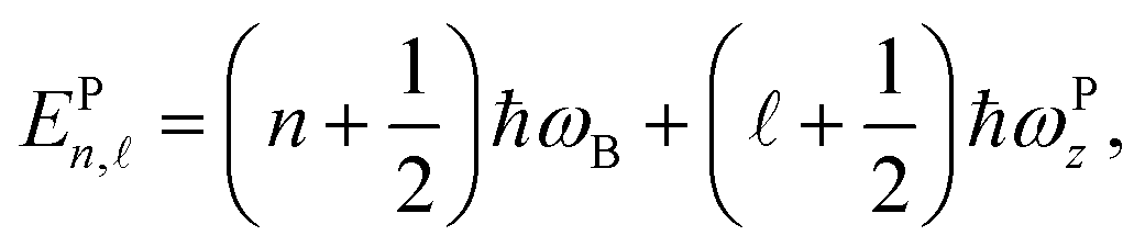
We consider the two QW models that are parabolic and semi-parabolic QWs where charge carriers in both the y- and x-directions are considered to be free. The charge carrier confinement in the z-direction of the parabolic and semiparabolic QW models is characterized using the two terms UP(z) and US(z), respectively. Applying an EMF which is given by B = Bẑ to the two quantum-well models and at the same time utilizing the approximation model of the electronic effective mass in the conduction band, the eigenfunction ΨNn is revealed as follows:23,24,45,46| | Φ(n,![[small script l]](https://www.rsc.org/images/entities/i_char_e146.gif) ) = Ly−1/2φn(x − x0)eikyyχ(z), ) = Ly−1/2φn(x − x0)eikyyχ(z), | (1) |
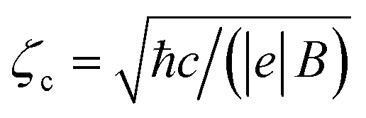
In the expression of Φ(n, ), the symbols are explained as follows: n, , and φn(x − x0) stand for the Landau levels (LLs), electrical sub-band levels, and the harmonic-oscillator function of the charge carrier in the semiparabolic and parabolic QW models, centred at x0 = −ζc2ky in which 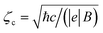 reveals the cyclotron radius. The electronic wave-function in the z-axis is symbolized by χ
![[small script l]](https://www.rsc.org/images/entities/char_e146.gif) (z) that depends on the confining potential U(z). The form of the potential describes the quantum confining potential of the electrons in a quantum well and is closely related to the quantum-well geometry shape. The electronic wave-functions are different for different confining potentials.
(z) that depends on the confining potential U(z). The form of the potential describes the quantum confining potential of the electrons in a quantum well and is closely related to the quantum-well geometry shape. The electronic wave-functions are different for different confining potentials.
For the parabolic confinement potential:
In the case of this potential, the term UP(z) is revealed by47–50
where
m* and
ωPz are symbols of the effective mass of the charge-carrier and the characteristic confining frequency of the parabolic-well electron. In this case, the eigenfunctions (
χP(
z)) and the corresponding eigenvalues (
EPn,) of the parabolic-well electron are given by
| |  | (3) |
and
| |  | (4) |
where the Hermite polynomials of order
are symbolized by
H(
z/
λz),
= 0, 1, 2, …, and
λz = (
ℏ/(
m*
ωPz))
1/2.
ωc = |
e|
B/(
m*
c) is the cyclotron frequency in which
e is the electron charge.
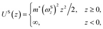
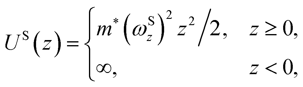
For the semi-parabolic confinement potential:
In the case of this potential, the term US(z) is revealed as51–53
| |  | (5) |
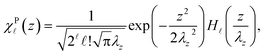
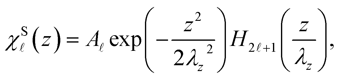
where
ωSz is the symbol of the characteristic confining frequency of the semi-parabolic-well electron. In this case, the eigenfunctions (
χS(
z)) and the corresponding eigenvalues (
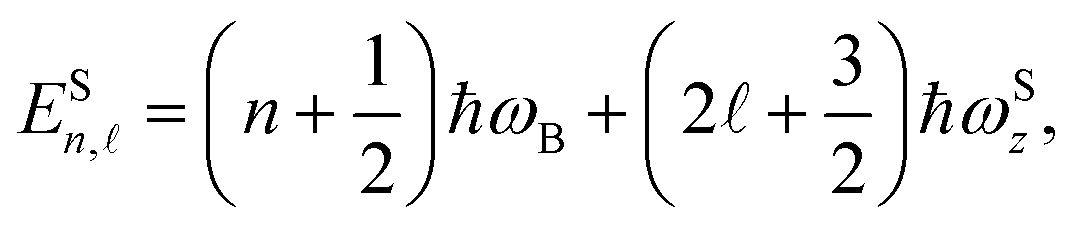
ESn,) of the semi-parabolic-well electron are given by
| |  | (6) |
and
| |  | (7) |
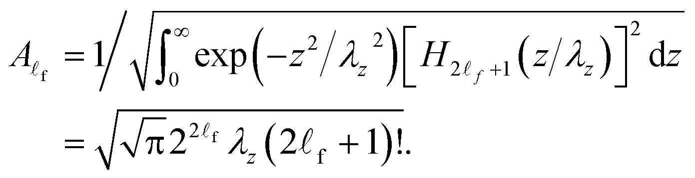
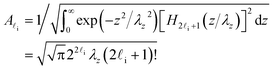
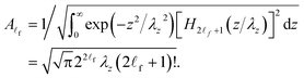
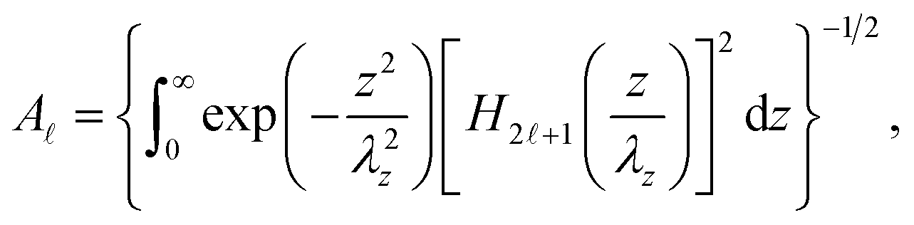
Here, the normalization factor is symbolized by
An, and it takes the form
| |  | (8) |
where Hermite polynomials of order (2
+ 1) are displayed using
H2+1(
z/
λz).
2.2. Electron–acoustic-phonon interaction matrix elements in parabolic and semi-parabolic QWs
We consider the matrix-element of EAP interaction in the parabolic and semi-parabolic QWs which takes the form of23,45,54–59| | 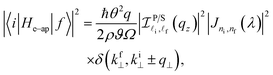 | (9) |
where θ, ρ, and ϑ stand respectively for the deformation potential constant, the material mass density, and the sound velocity in the material. The factors Ω and q respectively are the quantum-well's volume and the wave-vector of the acoustic-phonon. Finally, the two terms include  and |Jni,nf(λ)|2 in eqn (9), and they take the form:
| | 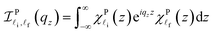 | (10) |
for the parabolic QW and| | 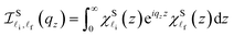 | (11) |
for the semi-parabolic QW, and| |  | (12) |
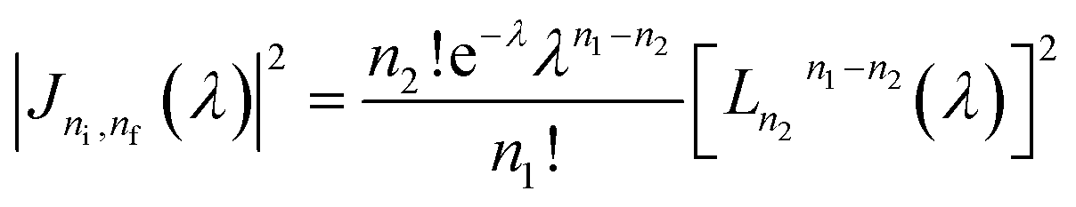
where  is the Laguerre polynomial with λ = ζc2q2⊥/2, n1 = max{ni, nf}, and n2 = min{ni, nf}. The two terms
  and
and  are the overlap integrals of the EAP interaction in the parabolic and semi-parabolic QWs, respectively.
3. Analytical computation of the acoustic-phonon-assisted CR absorption power in both the parabolic and semi-parabolic QWs
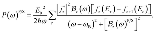
In this section, the acoustic-phonon-assisted CR absorption power in both the parabolic and semiparabolic QWs under the effect of an EMF will be computed in detail, where electronic systems in both the semiparabolic and parabolic QWs are placed in the EMF which is polarized circularly in the y − x-plane. Here, we assume that the EMF has an amplitude of E0 and a frequency of ω, and at the same time the EMF is incident upon the parabolic and semi-parabolic QW electron systems that are considered to be confined in the z-axis. Then, the acoustic-phonon-assisted CR absorption power in both the parabolic and semi-parabolic QWs is presented by60,61| | | P(ω)=E02Re{ϒ+−(ω)}/2, | (13) |
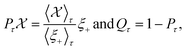
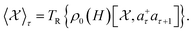
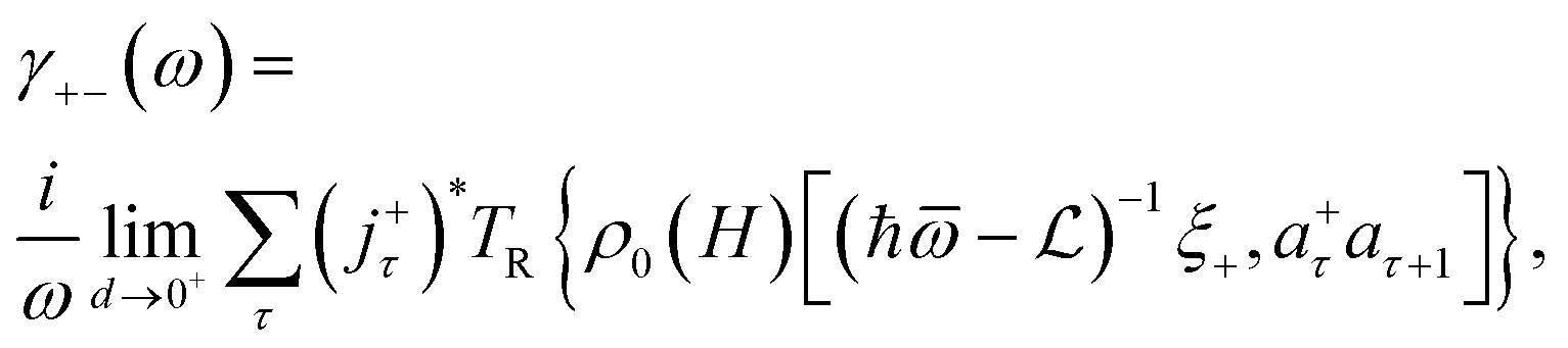
In expression (13), the conductivity tensor (CT) of the semiparabolic and parabolic QW electron systems with the real part is set by Re{ϒ+−(ω)} that is caused by the EAP interaction under the effect of the EMF. In the next step in this work, we will perform a detailed calculation of the term Re{ϒ+−(ω)} in eqn (13). Under the considerable effect of the EMF, the CT of the parabolic and semi-parabolic QW electron systems, ϒ+−(ω), is revealed using the following equation60–63| |  | (14) |
where ∑τ⋯ → ∑n∑⋯,  . TR and ρ0(H) are the many body traces and the electronic density operator.
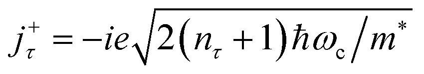
 ![[small omega, Greek, macron]](https://www.rsc.org/images/entities/i_char_e0da.gif) = ω − id with d → 0+ and ξ+ = ξx + iξy stands for the electronic current-operator, and a+τ/aτ+1 stands for the operators for an electronic creation/annihilation. The relation of the Liouville operator
= ω − id with d → 0+ and ξ+ = ξx + iξy stands for the electronic current-operator, and a+τ/aτ+1 stands for the operators for an electronic creation/annihilation. The relation of the Liouville operator  is directly related to the relation of the Hamiltonian
  , in which the first term,
  , and the second term,
  , are respectively the unperturbed component and perturbed component. When a QW is subjected to an EMF in the z-axis, the
  of this quantum system can be expressed as:
| | 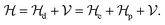 | (15) |
where  and
and  take the form
| |  | (16) |
and  is given by
| | 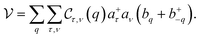 | (17) |
Here, b+q/bq reveals the operator for a phonon creation/annihilation. In eqn (17), the matrix-element for el–ph interaction is denoted by  , given by
| | 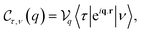 | (18) |
with  being the coupling factor.
In the present investigation, we used the operator projection (OP) method to study the CR absorption power in parabolic and semi-parabolic QWs with acoustic-phonon assistance. When it comes to MO transition problems, the OP method is a popular approach. This is because the MO-conductivity formalisms make the linear response theory acceptable. The weak time-dependent perturbation caused by electromagnetic radiation is a contributing factor. Moreover, the significant advantage of this method is that it allows us to obtain the explicit line-width function expression, as presented in eqn (26) and (A.2), where their terms can describe the able transitions of an electron in QWs with obvious physical meaning. This method expression is defined as
| |  | (19) |
where

is an arbitrary operator, and

is defined by
| |  | (20) |
Using the relation which is given by eqn (20), we rewrite eqn (14) as:
| |  | (21) |
In the next step, the term  in eqn (21) will be computed based on the relation: (A − B)−1 = A−1 + A−1B(A − B)−1 and eqn (19). Finally, we obtained
| |  | (22) |
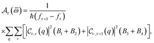
The Fermi level is denoted by the value of EF in the equation represented by fτ(Eτ) = 1/{exp[(Eτ − EF)/kBT] + 1}, which is the distribution function of the Fermi-Dirac function, and  is given by
| |  | (23) |
Here,

and

are given by
eqn (18) and the terms
B1,
B2,
B3, and
B4 are given by
eqn (A.1) of Appendix A.
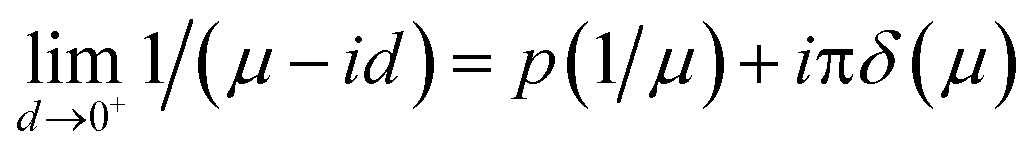
In the present work, we utilize the following approximation for the acoustic phonons: ϕq + 1 ≈ ϕq ≈ kBT/(ℏωq) where ωq = ϑq, and the energy of the acoustic phonon satisfies the condition ℏωq ≪ ℏωB. Another important notice is that  is the complex quantity that is because of = ω − id. Thus, we can also write as
  where
where  and
and  are the corresponding shift and linewidth of the acoustic-phonon-assisted CR-absorption peak. In this work, however, we focus on computing the absorption-power and the FWHM because of the EAP interaction in the above quantum systems for both the GaN and GaAs materials. Hence, in the quantum limit, the term
  can be neglected. Finally, the explicit expression of Re{ϒ+−(ω)} for the semiparabolic and parabolic QW electron systems is obtained as
| |  | (24) |
Using
eqn (24) and
(13), we obtain the acoustic-phonon-assisted CR absorption power of the electron in both the parabolic and semi-parabolic QWs for both GaN and GaAs materials, presented by
| |  | (25) |
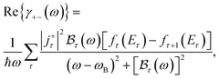
By using the Dirac identity, 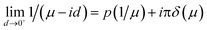 , and eqn (23), finally we obtain the linewidth-function expression,
  , for the EAP interaction in both the semiparabolic and parabolic QWs for both kinds of materials GaAs and GaN as follows:
| | 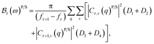 | (26) |
where the terms
D1,
D2,
D3, and
D4 are given by
eqn (A.2) of Appendix A.
By using the approximations for the acoustic phonons which are above mentioned and the following relationship
| |  | (27) |
to calculate the matrix elements for the EAP interaction |
Cτ,ν(
q)|
2 and |
Cτ+1,ν(
q)|
2, and related quantities in
eqn (26), we finally obtain the explicit linewidth-function expression,

, for the EAP interaction in both the parabolic and semi-parabolic QWs for both GaN and GaAs materials, as given by
eqn (A.3) of Appendix A. In
eqn (A.3), the Dirac delta functions include
δ(
EP/S1) and
δ(
EP/S2) which will be replaced by the corresponding Lorentzians of width
βP/Sn,n′ and
βP/Sn+1,n′, which are revealed by the two following equations:
64| |  | (28) |
| | 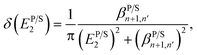 | (29) |
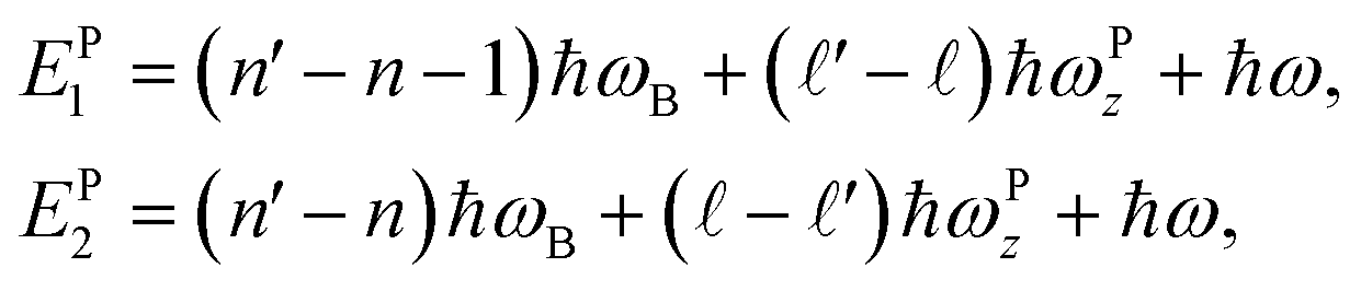
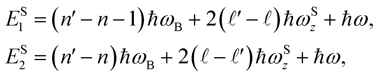
with the two terms
EP/S1 and
EP/S2 given by
| |  | (30) |
| |  | (31) |
and
| |  | (32) |
where
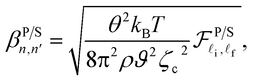
| |  | (33) |
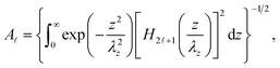
In order to achieve the aforementioned main aim of this work, we must calculate precisely the overlap-integral,  , in eqn (33) for both the parabolic and semi-parabolic QWs. After making systematical calculations, we have finally obtained the results for the parabolic and semi-parabolic wells, as shown in eqn (B.1) and (B.2) of Appendix B. Note that the overlap integral,
  , in expression (B.2) for the EAP interaction in the semi-parabolic QW will be numerically evaluated precisely. Utilizing the above analytic computation results, we apply appropriate computational techniques for the numerical calculations on the GaN and GaAs materials to get reliable results of the number crunching as well as the graphs in both the parabolic and semi-parabolic QWs; the physical summary of the investigation of the comparison of the EAP interaction strength in parabolic and semi-parabolic QWs for both GaN and GaAs materials will be provided in the below section.
4. Numerical results and discussion
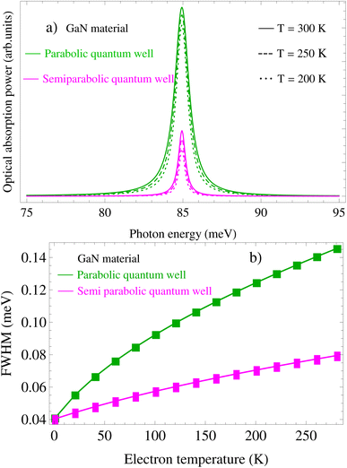
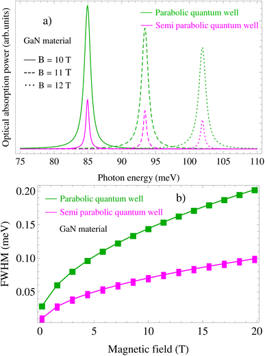
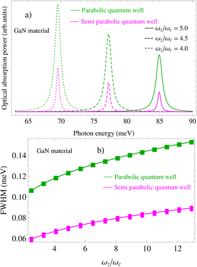
To clarify the difference in the EAP interaction strength between the symmetric (parabolic) and asymmetric (semiparabolic) quantum-wells for both GaN and GaAs materials, the numerical calculations on the GaN and GaAs materials have been carried out with the values of parameters:40θ = 12.42 eV, ρ = 5.31 g cm−3, ϑ = 5.22 × 105 cm s−1, and m* = 0.0667 × m0 for the GaAs material and θ = 10.0 eV, ρ = 6.1 g cm−3, ϑ = 4.57 × 105 cm s−1, and m* = 0.15 × m0 for the GaN material. Finally, we obtained some important results as below:
In Fig. 1(a) and 5(a), we respectively plot the dependence of the acoustic-phonon-assisted CR absorption power in the parabolic and semi-parabolic QWs on the photon-energy for typical GaAs and GaN materials at a magnetic field of 10 T and an electron temperature of 300 K. Simultaneously, the dependence of the acoustic-phonon-assisted CR absorption power at the CR-peak in QWs with the inter-sub-band transition (peak 2) on the photon energy in the parabolic and semi-parabolic QWs for typical GaAs and GaN materials with an EMF of 10 T and an ET of 300 K is also revealed in Fig. 1(b) and 5(b). Here, the blue- and red-lines correspond to the parabolic and semi-parabolic QWs. We easily see from the two graphs in Fig. 1(a) and 5(a) that they have two resonant peaks which are numbered in detail from the number peak (1) to the number peak (2) with their corresponding descriptions as follows: the CR-condition is described by the equation ℏωP/S = (n′ − n)ℏωc for both the GaAs and GaN materials in the parabolic and semi-parabolic QWs which is satisfied by the number peak (1) and determined using a ℏω of 17.37 (meV) for a typical GaAs material and of 7.72 (meV) for a typical GaN material. This number peak (1) in the parabolic and semi-parabolic QWs refers to an electron at LL n = 0 for both the GaAs and GaN materials that absorbs one ℏω to move to LL n′ = 1. The number peak (2) in the parabolic and semi-parabolic QWs is revealed in the two above figures which satisfy the CR-condition with an inter-sub-band transition between the levels = 0, 1 for both the parabolic and semi-parabolic QWs and is described by the equation ℏωP/S = (n′ − n)ℏωc + (′ − )ℏωP/Sz for both the GaAs and GaN materials, and it is determined using a ℏω of 191.01 (meV) for a typical GaAs material and of 84.94 (meV) for a typical GaN material. The main aim of this investigation is to carry out a detailed investigation on the comparison of the EAP interaction strength in the parabolic and semi-parabolic QWs for both the GaN and GaAs materials. Therefore, we only choose one of the two above peaks to examine the EAP interaction strength by measuring the FWHM of the acoustic-phonon-assisted CR-absorption peak, and hence for convenience, the number peak (2) which satisfies the CR-condition with an inter-sub-band transition between the levels = 0, 1 for both the semiparabolic and parabolic QWs is used in order to measure the FWHM in the semiparabolic and parabolic QWs for both the GaN and GaAs materials. In addition, for convenience in the clear observability of the number peak (2) of the semiparabolic and parabolic QWs for the GaN and GaAs materials, we separated this resonance peak from those in Fig. 1(a) and 5(a) as is clearly shown in Fig. 1(b) and 5(b).
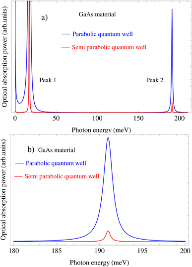 |
| | Fig. 1 (a) Photon-energy (ℏω) dependence of the acoustic-phonon-assisted CR absorption power in the parabolic and semi-parabolic QWs for a typical GaAs material at a magnetic-field of 10 T and an electron temperature of 300 K. (b) Dependence of the acoustic-phonon-assisted CR absorption power at the CR-peak with the inter-sub-band transition (peak 2) on the photon energy in the parabolic and semi-parabolic QWs for a typical GaAs material at a magnetic-field of 10 T and an electron temperature of 300 K. | |
In this work, the ℏω-dependence of the acoustic-phonon-assisted CR absorption power at the CR-peak with the inter-sub-band transition for the different electron temperatures, the different magnetic fields, and the different confining frequencies in both the semiparabolic and parabolic QWs is plotted in Fig. 2(a), 3(a), and 4(a) for the GaAs material and in Fig. 6(a), 7(a), and 8(a) for the GaN material, respectively. Fig. 2(a) and 6(a) show that the positions of the acoustic-phonon-assisted CR absorption power at the CR-peak with the inter-sub-band transition in the parabolic and semi-parabolic QWs for both the GaN and GaAs materials are not affected obviously by the ET of the electron; however, the ET of the electron strongly affects the strengths of the acoustic-phonon-assisted CR absorption power at the CR-peak with the inter-sub-band transition in the parabolic and semi-parabolic QWs for both the GaN and GaAs materials, i.e., with the increasing ET of the electron, the positions of the acoustic-phonon-assisted CR absorption power at the CR-peak with the inter-sub-band transition in the parabolic and semi-parabolic QWs are always unchanged for both the two types of materials GaN and GaAs, but their strengths are found to increase for both kinds of materials GaAs and GaN. The explanation of this property in the semiparabolic and parabolic QWs is that the Dirac delta functions δ(EP/S1,2) in eqn (A.3) which have the arguments EP1 = (n′ − n − 1)ℏωc + (′ − )ℏωPz + ℏω, EP2 = (n′ − n)ℏωc + ( − ′)ℏωPz + ℏω, and ES1 = (n′ − n − 1)ℏωc + 2(′ − )ℏωSz + ℏω, ES2 = (n′ − n)ℏωc + 2( − ′)ℏωSz + ℏω as shown in eqn (30) and (31) are found clearly to not include T of the electron, while the distribution functions of the acoustic phonon ϕq + 1 ≈ ϕq ≈ kBT/(ℏωq) in both the two types of materials GaN and GaAs and of the confinement electron, fn,, by the parabolic and semi-parabolic potentials together contain ET of the electron. On the other hand, as the ET of the semi-parabolic and parabolic QW systems increases, the strength of the interaction between electrons and acoustic phonons also increases. This implies that the scattering probability increases with the ET. Another very important point is that under the influence of the electronic temperature, the intensity of the acoustic-phonon-assisted CR absorption power at the CR-peak with the inter-sub-band transition in both kinds of materials GaAs and GaN of the parabolic potential QW is always more strong than that of the semi-parabolic potential QW. The explanation for this property is that the parabolic potential QW is a symmetric system while the semi-parabolic potential QW is an asymmetric one. This property will be useful for several potential application investigations for optoelectronic devices.
 |
| | Fig. 2 (a) Photon-energy dependence of the acoustic-phonon-assisted CR absorption power at the CR-peak with the inter-sub-band transition for different electron temperatures in the parabolic and semi-parabolic QWs for a typical GaAs material at a magnetic field of 10 T. (b) Dependence of the EAP interaction strength in the parabolic and semi-parabolic QWs for a typical GaAs material on the electron temperature at a magnetic field of 10 T. | |
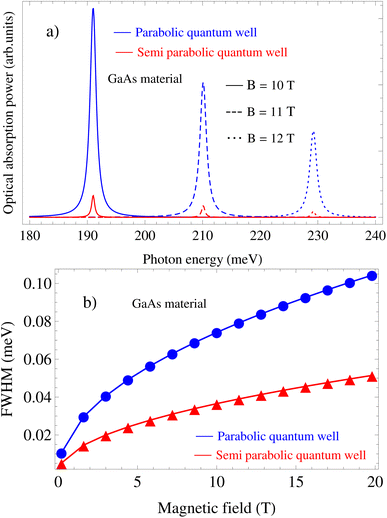 |
| | Fig. 3 (a) Photon-energy dependence of the acoustic-phonon-assisted CR absorption power at the CR-peak with the inter-sub-band transition for different magnetic fields in the parabolic and semi-parabolic QWs for a typical GaAs material at an electron temperature of 300 K. (b) Dependence of the EAP interaction strength in the parabolic and semi-parabolic QWs for a typical GaAs material on the magnetic field at an electron temperature of 300 K. | |
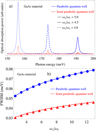 |
| | Fig. 4 (a) Photon-energy dependence of the acoustic-phonon-assisted CR absorption power at the CR-peak with the inter-sub-band transition for different confining frequencies in the parabolic and semi-parabolic QWs for a typical GaAs material at a magnetic field of 10 T and an electron temperature of 300 K. (b) Dependence of the EAP interaction strength in the parabolic and semi-parabolic QWs for a typical GaAs material on the confining frequency at a magnetic field of 10 T and an electron temperature of 300 K. | |
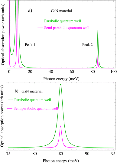 |
| | Fig. 5 (a) Photon-energy dependence of the acoustic-phonon-assisted CR absorption power in the parabolic and semi-parabolic QWs for a typical GaN material at a magnetic field of 10 T and an electron temperature of 300 K. (b) Dependence of the acoustic-phonon-assisted CR absorption power at the CR-peak with the inter-sub-band transition (peak 2) on the photon energy in the parabolic and semi-parabolic QWs for a typical GaN material at a magnetic field of 10 T and an electron temperature of 300 K. | |
 |
| | Fig. 6 (a) Photon-energy dependence of the acoustic-phonon-assisted CR absorption power at the CR-peak with the inter-sub-band transition for different electron temperatures in the parabolic and semi-parabolic QWs for a typical GaN material at a magnetic field of 10 T. (b) Dependence of the EAP interaction strength in the parabolic and semi-parabolic QWs for a typical GaN material on the electron temperature at a magnetic field of 10 T. | |
 |
| | Fig. 7 (a) Photon-energy dependence of the acoustic-phonon-assisted CR absorption power at the CR-peak with the inter-sub-band transition for different magnetic fields in the parabolic and semi-parabolic QWs for a typical GaN material at an electron temperature of 300 K. (b) Dependence of the EAP interaction strength in the parabolic and semi-parabolic QWs for a typical GaN material on the magnetic field at an electron temperature of 300 K. | |
 |
| | Fig. 8 (a) Photon-energy dependence of the acoustic-phonon-assisted CR absorption power at the CR-peak with the inter-sub-band transition for different confining frequencies in the parabolic and semi-parabolic QWs for a typical GaN material at a magnetic field of 10 T and an electron temperature of 300 K. (b) Dependence of the EAP interaction strength in the parabolic and semi-parabolic QWs for a typical GaN material on the confining frequency at a magnetic field of 10 T and an electron temperature of 300 K. | |
Moreover, Fig. 3(a), 7(a),4(a), and 8(a) show that the positions of the acoustic-phonon-assisted CR absorption power at the CR-peak with the inter-sub-band transition in the parabolic and semi-parabolic QWs for both the GaN and GaAs materials are obviously affected by the external magnetic field (EMF) and the confined potential frequency (CPF), i.e., with the increasing-EMF as well as the increasing-CPF, the positions and strengths of the acoustic-phonon-assisted CR absorption power at the CR-peak with the inter-sub-band transition in the parabolic and semi-parabolic QWs respectively are blue-shifted considerably and decrease strongly for both kinds of materials GaAs and GaN. This is the reason for the CR-condition with an inter-sub-band transition between the levels = 0, 1 for both the parabolic and semi-parabolic QWs and is described by the equation ℏωP/S = (n′ − n)ℏωc + (′ − )ℏωP/Sz for both the GaAs and GaN materials. This equation demonstrated that the CR-condition with an inter-sub-band transition between the levels = 0, 1 for both the GaN and GaAs materials in the parabolic and semi-parabolic QWs explicitly depend on both the magnetic field and confined potential frequency, and at the same time the photon energies are absorbed by the confined electron in the parabolic and semi-parabolic QWs at these CR-peaks with an inter-sub-band transition are directly proportional to both the magnetic field and confined potential frequency wherefore with the increasing-EMF as well as the increasing-CPF, the positions and strengths of the acoustic-phonon-assisted CR absorption power at the CR-peak with the inter-sub-band transition in the parabolic and semi-parabolic QWs are blue-shifted remarkably and strongly decreased, respectively for both kinds of materials GaAs and GaN. In addition, the increase of the EMF and the CPF yields an increment in the strengths of the acoustic-phonon-assisted CR absorption power at the CR-peak with the inter-sub-band transition in the parabolic and semi-parabolic QWs because the EAP scattering probability augments for both the GaN and GaAs materials.
In order to clarify the significant contribution from acoustic-phonon mode to the EAP interaction strength in the semiparabolic and parabolic QWs under the influence of the ET, EMF, and CPF, we plotted the corresponding graphs as shown in Fig. 2(b), 3(b), and 4(b) for the GaAs material and in Fig. 6(b), 7(b), and 8(b) for the GaN material. In this work, the spectral FWHM is investigated in the large range of the ET, EMF, and CPF parameters, including 77 K and 300 K, 5 T and 10 T, and ωz = ωc with the expectation that optoelectronic device applications can benefit from information on the above two QWs. Additionally, these findings may serve as an orientation for future experimental research. The dependence of the EAP interaction strength in both the parabolic and semi-parabolic QWs for the corresponding GaAs and GaN materials on the electron temperature at a magnetic field of 10 T is revealed in Fig. 2(b) and 6(b). Besides, Fig. 3(b) and 7(b) reveal the dependence of the EAP interaction strength in both the parabolic and semi-parabolic QWs for the corresponding GaAs and GaN materials on the EMF at an electron temperature of 300 K. In addition, Fig. 4(b) and 8(b) refer to the dependence of the EAP interaction strength in the parabolic and semi-parabolic QWs for the corresponding GaAs and GaN materials on the confining frequency at an EMF of 10 T and an ET of 300 K. Based on the obtained graphs, we can remark that the EAP interaction strength in the semiparabolic and parabolic QWs under the influence of the ET, EMF, and CPC always augments as the ET, the EMF, and the CPF increase for both kinds of materials GaAs and GaN. This is because the increasing ET, the increasing EMF and the increasing CPF will yield an increment in the EAP scattering probability in both the GaN and GaAs materials. In comparison with the previous experimental research studies as shown in ref. 65–71, our results are found to be consistent with them. In addition, the EAP interaction strength in the semi-parabolic and parabolic QWs always augments as the confining frequency of the symmetric (parabolic) and asymmetric (semi-parabolic) potential increases for both kinds of materials GaAs and GaN; this is because the quantum confinement intensity of the symmetric and asymmetric QW electrons will be stronger when increasing their confining frequencies. In comparison with the previous experimental research studies as shown in ref. 65, 68, and 72–74, our results are found to be well consistent with them. Moreover, Fig. 3(b) and 7(b) reveal that the EAP interaction strength in both the parabolic and semi-parabolic QWs for both the GaAs and GaN materials always augments as the EMF increases. This is because the EMF-dependence of the ζc cyclotron radius through the equation of ζc is revealed by 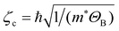 where ΘB = eℏB/m*. Thus, the augmentation of the EMF will yield a decrement in
  , which brings an increment in the electronic confinement intensity in the semiparabolic and parabolic QWs for both kinds of materials GaAs and GaN, and hence the EAP scattering probability in the semi-parabolic and parabolic QWs for both kinds of materials GaAs and GaN increases, wherefore the EAP interaction strength in the semiparabolic and parabolic QWs increases obviously with the increasing EMF for both kinds of materials GaAs and GaN. In comparison with the previous experimental research studies as shown in ref. 65 and 72, our results are found to be well consistent with them. In particular, by comparing the EAP interaction strength between the parabolic and semi-parabolic QWs for both the GaAs and GaN materials as shown in Fig. 2(b), 3(b), and 4(b) for the GaAs material and in Fig. 6(b),7(b), and 8(b) for the GaN material, we realize that there is a remarkable difference in the EAP interaction strength between the parabolic and semi-parabolic QWs, i.e., the EAP interaction strengths in the parabolic QW are always stronger than those in the semi-parabolic QW for both the GaAs and GaN materials. This is because the parabolic QW is a type of system that is symmetrical and has energy subbands that are equally spaced. This results in a build-up of radiation at a specific frequency determined by the distance between intersubbands. Simultaneously, the parity-allowed interband carrier transitions exhibit improvement in the parabolic QW. Meanwhile, the semi-parabolic QW is a type of system that is asymmetrical. Additionally, Fig. 4(b) and 8(b) show that the FWHM increases with the increment of the QW confining frequency (ωz) in both the GaN and GaAs materials. This is due to the enhanced EAP scattering probability with an increase in ωz. The parabolic QWs possess features that could potentially result in favorable optical-magnetic properties, including the acoustic-phonon-assisted CR absorption power and the FWHM of the acoustic-phonon-assisted CR-peak in both kinds of materials GaN and GaAs, with the expectation that optoelectronic device applications can benefit from information on these QWs.
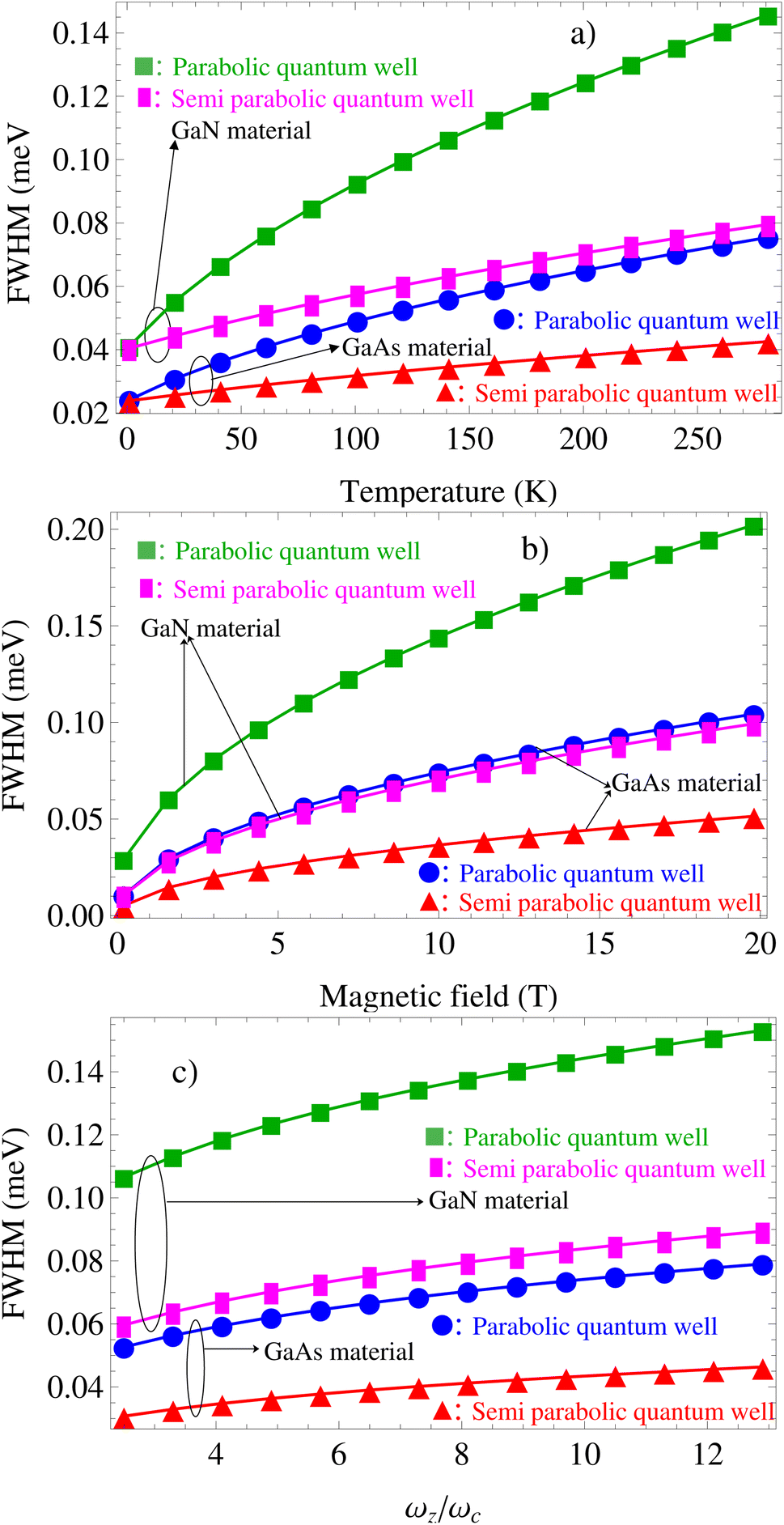
In particular, in Fig. 9, we have performed a detailed comparison of the dependence of the EAP interaction strength on the temperature (see in Fig. 9(a)), the magnetic field (see in Fig. 9(b)), and the confined-frequency (see in Fig. 9(c)) between the GaN and GaAs materials in both the semi-parabolic and parabolic potential QWs. We can see from Fig. 9(a)–(c) that the spectral FWHM of the cyclotron-resonance peak increases as the temperature, the external magnetic field, and the confining potential increase. The physical meaning of this phenomenon is that the electron-phonon scattering probability in both the GaN and GaAs materials increases as the temperature, the external magnetic field, and the confining potential increase for both the semi-parabolic and parabolic potential QWs. Moreover, we also easily understand that when the external magnetic field and the confining potential increase there is an increase in the confining strength of the electron wherefore the electron-phonon scattering probability increases. On the other hand, the comparative results revealed that under the effect of both the ET, the EMF, and the CPF, the EAP interaction strengths in the symmetric (parabolic) QW have larger values and they vary faster than they do in the asymmetric (semi-parabolic) QW for both kinds of materials GaAs and GaN; in other words, the EAP interaction strengths in the parabolic QW is always much stronger than that in the semi-parabolic QW for both GaN and GaAs materials. Furthermore, the EAP interaction strengths in the GaN material have larger values and they vary faster than they do in the GaAs material for both the parabolic and semi-parabolic QWs, i.e., the EAP interaction strength in the GaN material is always much stronger than that in the GaAs material for both the parabolic and semi-parabolic QWs. In addition, among the four graphs which describe the four EAP interaction strengths as shown in Fig. 9 under the effects of both the ET, the EMF, and the CPF, we can see that the EAP interaction strength in the GaN material of the parabolic QW is the strongest while it is weakest in the GaAs material of the semi-parabolic QW. Our results can demonstrate further that the MO-properties, including the EAP interaction strength in the symmetric (parabolic) GaN QW material, are remarkably different from those in the GaN material of the asymmetric (semi-parabolic) QW as well as in the GaAs material of the symmetric (parabolic) and asymmetric (semi-parabolic) QWs. These research results can be useful for several potential application investigations for optoelectronic devices.
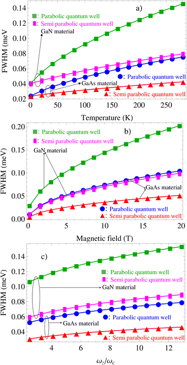 |
| | Fig. 9 Comparison of the dependence of the EAP interaction strength on the electron temperature (see in (a)), magnetic field (see in (b)), and confining frequency (see in (c)) between the GaN and GaAs materials in both the parabolic and semi-parabolic QWs. | |
5. Conclusions
We conducted a study to compare the EAP interaction strengths in the symmetric and asymmetric QWs for GaAs and GaN materials. By using the two main methods mentioned in the Abstract part, we obtained the main results as follows: the position of the acoustic-phonon-assisted CR absorption peak is still unchanging with increasing ET, but it has a blue shift with an increase in the CPF and the EMF. Besides, the EAP interaction strengths in the symmetric and asymmetric QWs depend strongly on both the structural parameters, such as the CPF, and the external parameters, such as the ET and the EMF, for both kinds of materials GaAs and GaN. This means that the EAP interaction strengths in the symmetric and asymmetric QWs for both kinds of materials GaAs and GaN increase with an increase in the CPF and the ET, and the EMF. Moreover, the obtained result demonstrated that within the dependence of the EAP interaction intensity on the ET, EMF, and CPF, the EAP interaction strength in the symmetric QW is always much stronger than that in the asymmetric QW for both GaN and GaAs materials. In addition, in comparison between the two GaN and GaAs materials, the result also showed that the EAP interaction strength in the GaN material is much stronger than that in the GaAs material for both the symmetric and asymmetric QW models. When it comes to optoelectronic devices, comparing the EAP interaction strength between the symmetric and asymmetric QWs in the GaN and GaAs materials can yield valuable properties.
Appendix A
| |
| (A.1) |
where ϕq = [exp(ℏωq/kBT) − 1]−1 is a symbol of the Planck distribution function in both the parabolic and semi-parabolic QWs. Here, kB and T are the Boltzmann constant and the temperature in Kelvin, respectively.| |  | (A.2) |
| |  | (A.3) |
Appendix B
For the parabolic (P) QW:| | 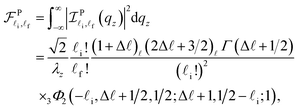 | (B.1) |
where 3Φ2(−i, Δ + 1/2, 1/2; Δ + 1, 1/2 − i; 1) is the hypergeometric function and Δ = f − i.
For the semi-parabolic (S) QW:
| | 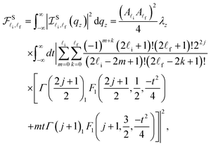 | (B.2) |
where
| |  | (B.3) |
and
| |  | (B.4) |
Data availability
Data available on request from the authors.
Author contributions
Tran Cong Phong: investigation, methodology, supervision, writing-review and editing, language editing, and funding acquisition. Le Ngoc Minh: software, investigation, conceptualization, supervision, writing-review and editing, language editing, and validation. Nguyen Dinh Hien: software, methodology, investigation, conceptualization, supervision, writing-original draft, writing-review and editing, validation, and funding acquisition.
Conflicts of interest
There are no conflicts to declare.
References
- P. Vasilopoulos, Magnetophonon oscillations in quasi-two-dimensional quantum wells, Phys. Rev. B: Condens. Matter Mater. Phys., 1986, 33, 8587–8594 CrossRef PubMed.
- S. Guo, Y. Zhang, Y. Ge, S. Zhang, H. Zeng and H. Zhang, 2D V-V binary materials: Status and challenges, Adv. Mater., 2019, 31(39), 1902352 CrossRef PubMed.
- J. He, L. Tao, H. Zhang, B. Zhou and J. Li, Emerging 2d materials beyond graphene for ultrashort pulse generation in fiber lasers, Nanoscale, 2019, 11, 2577–2593 RSC.
- J. Pei, J. Yang, T. Yildirim, H. Zhang and Y. Lu, Many-body complexes in 2d semiconductors, Adv. Mater., 2019, 31(2), 1706945 CrossRef PubMed.
- J. Du, M. Zhang, Z. Guo, J. Chen, X. Zhu, G. Hu, P. Peng, Z. Zheng and H. Zhang, Phosphorene quantum dot saturable absorbers for ultrafast fiber lasers, Sci. Rep., 2017, 7(42357), 1 Search PubMed.
- K. Van Nguyen and Y.-C. Chang, Full consideration of acoustic phonon scatterings in two-dimensional Dirac materials, Phys. Chem. Chem. Phys., 2020, 22, 3999–4009 RSC.
- K. Van Nguyen and Y.-C. Chang, Bloch-Grüneisen temperature and universal scaling of normalized resistivity in doped graphene revisited, Phys. Rev. B, 2021, 103, 045425 CrossRef CAS.
- S. Yu, K. W. Kim, M. A. Stroscio, G. J. Iafrate and A. Ballato, Electron–acoustic-phonon scattering rates in rectangular quantum wires, Phys. Rev. B: Condens. Matter Mater. Phys., 1994, 50, 1733–1738 CrossRef CAS.
- N. Mori and T. Ando, Electron–optical-phonon interaction in single and double heterostructures, Phys. Rev. B: Condens. Matter Mater. Phys., 1989, 40, 6175–6188 CrossRef PubMed.
- M. A. Stroscio, Interaction between longitudinal-optical-phonon modes of a rectangular quantum wire and charge carriers of a one-dimensional electron gas, Phys. Rev. B: Condens. Matter Mater. Phys., 1989, 40, 6428–6431 CrossRef PubMed.
- N. D. Hien, Comparison of the magneto-optical properties of the semi-parabolic well with those of the parabolic and rectangular wells under the combined influences of aluminum concentration and hydrostatic pressure, J. Phys. Chem. Solids, 2021, 110456 Search PubMed.
- W. Xu, Emission of acoustic and optical phonons by hot electrons in a two-dimensional electron system in parallel magnetic fields, Phys. Rev. B: Condens. Matter Mater. Phys., 1996, 54, 2775–2784 CrossRef CAS PubMed.
- M. A. Stroscio, G. J. Iafrate, K. W. Kim, M. A. Littlejohn, H. Goronkin and G. N. Maracas, Transition from longitudinal-optical phonon scattering to surface-optical phonon scattering in polar semiconductor superlattices, Appl. Phys. Lett., 1991, 59, 1093–1095 CrossRef CAS.
- M. A. Stroscio, Interface-phonon-assisted transitions in quantum-well lasers, J. Appl. Phys., 1996, 80, 6864–6867 CrossRef CAS.
- D. J. Barnes, R. J. Nicholas, F. M. Peeters, X.-G. Wu, J. T. Devreese, J. Singleton, C. J. G. M. Langerak, J. J. Harris and C. T. Foxon, Observation of optically detected magnetophonon resonance, Phys. Rev. Lett., 1991, 66, 794–797 CrossRef PubMed.
- N. Mori, H. Momose and C. Hamaguchi, Magnetophonon resonances in quantum wires, Phys. Rev. B: Condens. Matter Mater. Phys., 1992, 45, 4536–4539 CrossRef PubMed.
- G.-Q. Hai and F. M. Peeters, Optically detected magnetophonon resonances in gaas, Phys. Rev. B: Condens. Matter Mater. Phys., 1999, 60, 16513–16518 CrossRef CAS.
- S. Y. Choi, S. C. Lee, H. J. Lee, H. S. Ahn, S. W. Kim and J. Y. Ryu, Optically detected magnetophonon resonances in semiconductor based n-ge and n-gaas, Phys. Rev. B: Condens. Matter Mater. Phys., 2002, 66, 155208 CrossRef.
- S. C. Lee, H. S. Ahn, D. S. Kang, S. O. Lee and S. W. Kim, Optically detected magnetophonon resonances in n-ge in tilted magnetic fields, Phys. Rev. B: Condens. Matter Mater. Phys., 2003, 67, 115342 CrossRef.
- N. D. Hien, Magnetophonon resonance in quantum wells due to absorption and emission of confined phonon, Phys. E, 2019, 114, 113608 CrossRef.
- L. T. Q. Huong, L. N. Minh, N. T. Xuan Hoai and N. D. Hien, Magneto-optical transport properties of parabolic potential gaas wells under the influence of al concentration and hydrostatic pressure, Phys. E, 2021, 127, 114491 CrossRef CAS.
- N. D. Hien, Influence of the confining potential on the linewidth of a quantum well, Superlattices Microstruct., 2021, 160, 107068 CrossRef CAS.
- N. D. Hien, Combined influences of temperature, pressure, and alloy-composition on magneto-optical properties of the semi-parabolic well under all four different phonon models, Micro Nanostruct., 2022, 167, 207236 CrossRef CAS.
- N. D. Hien, Intersubband absorption linewidth in a semi-parabolic quantum well: Comparison among three different phonon models, Phys. B, 2022, 638, 413901 CrossRef CAS.
- C. Duque, M. Mora-Ramos and M. Barseghyan, Electronic states in a pöschl–teller-like quantum well: Combined effects of electric field, hydrostatic pressure, and temperature, Superlattices Microstruct., 2011, 50, 480–490 CrossRef CAS.
- N. D. Hien, C. Duque, E. Feddi, N. V. Hieu, H. D. Trien, L. T. Phuong, B. D. Hoi, L. T. Hoa, C. V. Nguyen, N. N. Hieu and H. V. Phuc, Magneto-optical effect in gaas/gaalas semi-parabolic quantum well, Thin Solid Films, 2019, 682, 10–17 CrossRef CAS.
- K. Doan Quoc and H. Nguyen Dinh, Influence of confined phonon for the different models in gaas quantum wells on the optically detected electrophonon resonance linewidth, Opt. Quantum Electron., 2019, 51, 116 CrossRef.
- C. V. Nguyen, N. N. Hieu, N. A. Poklonski, V. V. Ilyasov, L. Dinh, T. C. Phong, L. V. Tung and H. V. Phuc, Magneto-optical transport properties of monolayer mos2 on polar substrates, Phys. Rev. B, 2017, 96, 125411 CrossRef.
- N. D. Hien, C. V. Nguyen, N. N. Hieu, S. S. Kubakaddi, C. A. Duque, M. E. Mora-Ramos, L. Dinh, T. N. Bich and H. V. Phuc, Magneto-optical transport properties of monolayer transition metal dichalcogenides, Phys. Rev. B, 2020, 101, 045424 CrossRef.
- B. Hillebrands, S. Lee, G. I. Stegeman, H. Cheng, J. E. Potts and F. Nizzoli, Evidence for the existence of guided longitudinal acoustic phonons in znse films on gaas, Phys. Rev. Lett., 1988, 60, 832–835 CrossRef CAS PubMed.
- M. A. Stroscio and K. W. Kim, Piezoelectric scattering of carriers from confined acoustic modes in cylindrical quantum wires, Phys. Rev. B: Condens. Matter Mater. Phys., 1993, 48, 1936–1938 CrossRef CAS PubMed.
- Z. V. Popović, J. Spitzer, T. Ruf, M. Cardona, R. Nötzel and K. Ploog, Folded acoustic phonons in gaas/alas corrugated superlattices grown along the [311] direction, Phys. Rev. B: Condens. Matter Mater. Phys., 1993, 48, 1659–1664 CrossRef PubMed.
- H. Benisty, C. M. Sotomayor-Torrès and C. Weisbuch, Intrinsic mechanism for the poor luminescence properties of quantum-box systems, Phys. Rev. B: Condens. Matter Mater. Phys., 1991, 44, 10945–10948 CrossRef PubMed.
- N. Bannov, V. Mitin and M. Stroscio, Confined acoustic phonons in a free-standing quantum well and their interaction with electrons, Phys. Status Solidi B, 1994, 183, 131–142 CrossRef CAS , https://onlinelibrary.wiley.com.
- J. C. Nabity and M. N. Wybourne, Evidence for two-dimensional phonons in a thin metal film, Phys. Rev. B: Condens. Matter Mater. Phys., 1991, 44, 8990–8996 CrossRef.
- J. Seyler and M. N. Wybourne, Acoustic waveguide modes observed in electrically heated metal wires, Phys. Rev. Lett., 1992, 69, 1427–1430 CrossRef CAS.
- M. Rothenfusser, L. Köster and W. Dietsche, Phonon-emission spectroscopy of a two-dimensional electron gas, Phys. Rev. B: Condens. Matter Mater. Phys., 1986, 34, 5518–5524 CrossRef CAS.
- H. Lin, H. J. Maris, L. B. Freund, K. Y. Lee, H. Luhn and D. P. Kern, Study of vibrational modes of gold nanostructures by picosecond ultrasonics, J. Appl. Phys., 1993, 73, 37–45 CrossRef CAS.
- J. S. Bhat, R. A. Nesargi and B. G. Mulimani, Confined-acoustic-phonon-assisted cyclotron resonance in free-standing semiconductor quantum well structures, Phys. Rev. B: Condens. Matter Mater. Phys., 2006, 73, 235351 CrossRef.
- J. S. Bhat, R. A. Nesargi and B. G. Mulimani, Energy loss rate of hot electrons due to confined acoustic phonon modes in a freestanding quantum well structure, J. Appl. Phys., 2009, 106, 033701 CrossRef.
- M. S. B. Nam Lyong Kang, J. Y. Youn and E. J. Han, Calculation of the cyclotron transition line-width by confined phonon scattering using the projection-reduction method, Eur. Phys. J. B, 2015, 88, 01–07 Search PubMed.
- H. V. Phuc, L. Dinh and T. C. Phong, Phonon-assisted cyclotron resonance in quantum wells via the multiphoton absorption process, Superlattices Microstruct., 2013, 59, 77–86 CrossRef CAS.
- H. V. Phuc, N. T. T. Thao, L. Dinh and T. C. Phong, Confined-acoustic-phonon-assisted cyclotron resonance via multi-photon absorption process in gaas quantum well structure, J. Phys. Chem. Solids, 2014, 75, 300–305 CrossRef CAS.
- N. D. Hien, Intersubband and intrasubband electron scattering by acoustic-phonons in quantum wells, Optik, 2020, 206, 164348 CrossRef.
- N. D. Hien, Cyclotron resonance linewidth due to electron scattering by five different phonon modes in semiparabolic quantum wells, J. Phys. Chem. Solids, 2022, 167, 110757 CrossRef CAS.
- N. D. Hien, Comparison of the magneto-optical properties of the semi-parabolic well with those of the parabolic and rectangular wells under the combined influences of aluminum concentration and hydrostatic pressure, J. Phys. Chem. Solids, 2022, 161, 110456 CrossRef CAS.
- S. C. Lee, Y. B. Kang, D. C. Kim, J. Y. Ryu, N. L. Kang and S. D. Choi, Magnetophonon and electrophonon resonances in quantum wires, Phys. Rev. B: Condens. Matter Mater. Phys., 1997, 55, 6719–6722 CrossRef CAS.
- H. V. Phuc, N. N. Hieu, L. Dinh and T. C. Phong, Nonlinear optical absorption in parabolic quantum well via two-photon absorption process, Opt. Commun., 2015, 335, 37–41 CrossRef CAS.
- S. Chil Lee, J. Woo Kang, H. Soo Ahn, M. Yang, N. Lyong Kang and S. W. Kim, Optically detected electrophonon resonance effects in quantum wells, Phys. E, 2005, 28, 402–411 CrossRef.
- S. C. Lee, Optically Detected Magnetophonon Resonances in Quantum Wells, J. Korean Phys. Soc., 2007, 51, 1979 CrossRef CAS.
- L. Zhang and H.-J. Xie, Electric field effect on the second-order nonlinear optical properties of parabolic and semiparabolic quantum wells, Phys. Rev. B: Condens. Matter Mater. Phys., 2003, 68, 235315 CrossRef.
- C.-J. Zhang and K.-X. Guo, Polaron effects on the optical absorptions in asymmetrical semi-parabolic quantum wells, Phys. E, 2007, 39, 103–108 CrossRef CAS.
- X. Yu and Y. Yu, Optical absorptions in asymmetrical semi-parabolic quantum wells, Superlattices Microstruct., 2013, 62, 225–232 CrossRef CAS.
- J. S. Bhat, S. S. Kubakaddi and B. G. Mulimani, Cyclotron-phonon resonance in quasi-two-dimensional semiconducting structures, J. Appl. Phys., 1991, 70, 2216–2219 CrossRef CAS.
- Y. J. Cho and S. D. Choi, Calculation of quantum-limit cyclotron-resonance linewidths in ge and si by the isolation-projection technique, Phys. Rev. B: Condens. Matter Mater. Phys., 1994, 49, 14301–14306 CrossRef CAS.
- N. Kang, Y. Ji, H. J. Lee and S. Choi, Intraband linewidths of the optical conductivity in quantum wells due to lo phonon scattering, J. Korean Phys. Soc., 2003, 42, 379–385 CAS.
- N. Kang, Y. Lee and S. Choi, Derivation of the dc conductivity in a quantum well by using an operator algebra technique, J. Korean Phys. Soc., 2004, 44, 1535–1541 CAS.
- P. Vasilopoulos, Magnetophonon oscillations in quasi-two-dimensional quantum wells, Phys. Rev. B: Condens. Matter Mater. Phys., 1986, 33, 8587–8594 CrossRef PubMed.
- G.-Q. Hai and F. M. Peeters, Magnetopolaron
effect in parabolic quantum wells in tilted magnetic fields, Phys. Rev. B: Condens. Matter Mater. Phys., 1999, 60, 8984–8991 CrossRef CAS.
- J. Yon Ryu, Y. Choon Chung and S. Don Choi, Comparison of two techniques in the theory of phonon-induced cyclotron resonance line shapes, Phys. Rev. B: Condens. Matter Mater. Phys., 1985, 32, 7769–7775 CrossRef CAS PubMed.
- J. Y. Sug, S. G. Jo, J. Kim, J. H. Lee and S. D. Choi, Quantum transition processes in deformation potential interacting systems using the equilibrium density projection technique, Phys. Rev. B: Condens. Matter Mater. Phys., 2001, 64, 235210 CrossRef.
- N. L. Kang, S. D. Choi and Y. J. Cho, A Many-Body Theory of Quantum-Limit Cyclotron Transition Line-Shapes in Electron-Phonon Systems Based on Projection Technique, Prog. Theor. Phys., 1996, 96, 307–316 CrossRef CAS , http://oup.prod.sis.lan/ptp/article-pdf/96/2/307/5246478/96-2-307.pdf.
- N. Lyong Kang, J. H. Lee and D.-S. Choi, Calculation of cyclotron resonance linewidths in ge by using a many-body state-independent projection technique, J. Korean Phys. Soc., 2000, 37, 339–342 Search PubMed.
- M. P. Chaubey and C. M. Van Vliet, Transverse magnetoconductivity of quasi-two-dimensional semiconductor layers in the presence of phonon scattering, Phys. Rev. B: Condens. Matter Mater. Phys., 1986, 33, 5617–5622 CrossRef.
- M. Singh, Cyclotron-resonance linewidth due to electron-phonon interaction in multi-quantum-well structures, Phys. Rev. B: Condens. Matter Mater. Phys., 1987, 35, 9301–9304 CrossRef PubMed.
- T. Unuma, T. Takahashi, T. Noda, M. Yoshita, H. Sakaki, M. Baba and H. Akiyama, Effects of interface roughness and phonon scattering on intersubband absorption linewidth in a gaas quantum well, Appl. Phys. Lett., 2001, 78, 3448–3450 CrossRef CAS.
- P. von Allmen, M. Berz, G. Petrocelli, F. K. Reinhart and G. Harbeke, Inter-sub-band absorption in gaas/algaas quantum wells between 4.2 k and room temperature, Semicond. Sci. Technol., 1988, 3, 1211–1216 CrossRef CAS.
- T. Unuma, M. Yoshita, T. Noda, H. Sakaki and H. Akiyama, Intersubband absorption linewidth in gaas quantum wells due to scattering by interface roughness, phonons, alloy disorder, and impurities, J. Appl. Phys., 2003, 93, 1586–1597 CrossRef CAS.
- P. Voisin, Y. Guldner, J. P. Vieren, M. Voos, P. Delescluse and N. T. Linh, Cyclotron resonance linewidth in selectively doped gaas-algaas heterojunctions, Appl. Phys. Lett., 1981, 39, 982–984 CrossRef CAS.
- K. Muro, S. Mori, S. Narita, S. Hiyamizu and K. Nanbu, Cyclotron resonance of two-dimensional electrons in algaas/gaas heterojunction, Surf. Sci., 1984, 142, 394–399 CrossRef CAS.
- B. Tanatar and M. Singh, Temperature dependence of the cyclotron-resonance linewidth and effective mass in gaas/ga1−x alxas square-well structures, Phys. Rev. B: Condens. Matter Mater. Phys., 1991, 43, 6612–6619 CrossRef CAS PubMed.
- N. Holonyak, R. M. Kolbas, W. D. Laidig, M. Altarelli, R. D. Dupuis and P. D. Dapkus, Phonon-sideband mo-cvd quantum-well algaas-gaas heterostructure laser, Appl. Phys. Lett., 1979, 34, 502–505 CrossRef CAS.
- K. L. Campman, H. Schmidt, A. Imamoglu and A. C. Gossard, Interface roughness and alloy-disorder scattering contributions to intersubband transition linewidths, Appl. Phys. Lett., 1996, 69, 2554–2556 CrossRef CAS.
- M. Belmoubarik, K. Ohtani and H. Ohno, Intersubband transitions in zno multiple quantum wells, Appl. Phys. Lett., 2008, 92, 191906 CrossRef.
|
| This journal is © The Royal Society of Chemistry 2024 |
Click here to see how this site uses Cookies. View our privacy policy here. 
 Open Access Article
 This Open Access Article is licensed under a Creative Commons Attribution-Non Commercial 3.0 Unported Licence
 *de
*de
 reveals the cyclotron radius. The electronic wave-function in the z-axis is symbolized by χ

 and |Jni,nf(λ)|2 in eqn (9), and they take the form:
 is the Laguerre polynomial with λ = ζc2q2⊥/2, n1 = max{ni, nf}, and n2 = min{ni, nf}. The two terms
  and
and  are the overlap integrals of the EAP interaction in the parabolic and semi-parabolic QWs, respectively.
 . TR and ρ0(H) are the many body traces and the electronic density operator.
  is directly related to the relation of the Hamiltonian
  , in which the first term,
  , and the second term,
  , are respectively the unperturbed component and perturbed component. When a QW is subjected to an EMF in the z-axis, the
  of this quantum system can be expressed as:
 and
and  take the form
 is given by
 , given by
 being the coupling factor.

 is an arbitrary operator, and
  is defined by
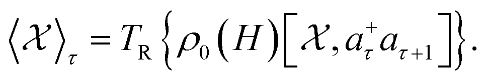

 in eqn (21) will be computed based on the relation: (A − B)−1 = A−1 + A−1B(A − B)−1 and eqn (19). Finally, we obtained
 is given by
 and
and  are given by eqn (18) and the terms B1, B2, B3, and B4 are given by eqn (A.1) of Appendix A.
 is the complex quantity that is because of
  where
where  and
and  are the corresponding shift and linewidth of the acoustic-phonon-assisted CR-absorption peak. In this work, however, we focus on computing the absorption-power and the FWHM because of the EAP interaction in the above quantum systems for both the GaN and GaAs materials. Hence, in the quantum limit, the term
  can be neglected. Finally, the explicit expression of Re{ϒ+−(ω)} for the semiparabolic and parabolic QW electron systems is obtained as

 , and eqn (23), finally we obtain the linewidth-function expression,
  , for the EAP interaction in both the semiparabolic and parabolic QWs for both kinds of materials GaAs and GaN as follows:

 , for the EAP interaction in both the parabolic and semi-parabolic QWs for both GaN and GaAs materials, as given by eqn (A.3) of Appendix A. In eqn (A.3), the Dirac delta functions include δ(EP/S1) and δ(EP/S2) which will be replaced by the corresponding Lorentzians of width βP/Sn,n′ and βP/Sn+1,n′, which are revealed by the two following equations:64
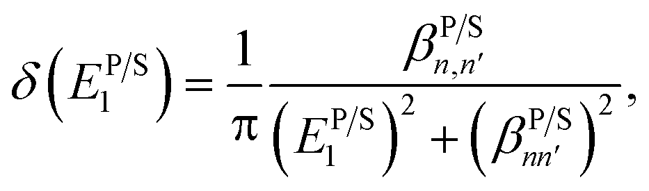


 , in eqn (33) for both the parabolic and semi-parabolic QWs. After making systematical calculations, we have finally obtained the results for the parabolic and semi-parabolic wells, as shown in eqn (B.1) and (B.2) of Appendix B. Note that the overlap integral,
  , in expression (B.2) for the EAP interaction in the semi-parabolic QW will be numerically evaluated precisely. Utilizing the above analytic computation results, we apply appropriate computational techniques for the numerical calculations on the GaN and GaAs materials to get reliable results of the number crunching as well as the graphs in both the parabolic and semi-parabolic QWs; the physical summary of the investigation of the comparison of the EAP interaction strength in parabolic and semi-parabolic QWs for both GaN and GaAs materials will be provided in the below section.


 where ΘB = eℏB/m*. Thus, the augmentation of the EMF will yield a decrement in
  , which brings an increment in the electronic confinement intensity in the semiparabolic and parabolic QWs for both kinds of materials GaAs and GaN, and hence the EAP scattering probability in the semi-parabolic and parabolic QWs for both kinds of materials GaAs and GaN increases, wherefore the EAP interaction strength in the semiparabolic and parabolic QWs increases obviously with the increasing EMF for both kinds of materials GaAs and GaN. In comparison with the previous experimental research studies as shown in ref. 65 and 72, our results are found to be well consistent with them. In particular, by comparing the EAP interaction strength between the parabolic and semi-parabolic QWs for both the GaAs and GaN materials as shown in Fig. 2(b), 3(b), and 4(b) for the GaAs material and in Fig. 6(b),7(b), and 8(b) for the GaN material, we realize that there is a remarkable difference in the EAP interaction strength between the parabolic and semi-parabolic QWs, i.e., the EAP interaction strengths in the parabolic QW are always stronger than those in the semi-parabolic QW for both the GaAs and GaN materials. This is because the parabolic QW is a type of system that is symmetrical and has energy subbands that are equally spaced. This results in a build-up of radiation at a specific frequency determined by the distance between intersubbands. Simultaneously, the parity-allowed interband carrier transitions exhibit improvement in the parabolic QW. Meanwhile, the semi-parabolic QW is a type of system that is asymmetrical. Additionally, Fig. 4(b) and 8(b) show that the FWHM increases with the increment of the QW confining frequency (ωz) in both the GaN and GaAs materials. This is due to the enhanced EAP scattering probability with an increase in ωz. The parabolic QWs possess features that could potentially result in favorable optical-magnetic properties, including the acoustic-phonon-assisted CR absorption power and the FWHM of the acoustic-phonon-assisted CR-peak in both kinds of materials GaN and GaAs, with the expectation that optoelectronic device applications can benefit from information on these QWs.