
 Open Access Article
 This Open Access Article is licensed under a
 Creative Commons Attribution 3.0 Unported Licence
An amorphous Cr2Ge2Te6/polyimide double-layer foil with an extraordinarily outstanding strain sensing ability
Yinli
Wang
 a,
Yi
Shuang
b,
Mihyeon
Kim
a,
Daisuke
Ando
a,
Fumio
Narita
c and
Yuji
Sutou
*ab
a,
Yi
Shuang
b,
Mihyeon
Kim
a,
Daisuke
Ando
a,
Fumio
Narita
c and
Yuji
Sutou
*ab
aDepartment of Materials Science, Graduate School of Engineering, Tohoku University, 6-6-11 Aoba-yama, Sendai, 980-8579, Japan. E-mail: ysutou@material.tohoku.ac.jp
bWPI Advanced Institute for Materials Research, Tohoku University, 2-1-1 Katahira, Aoba, Sendai, 980-8577, Japan
cDepartment of Frontier Sciences for Advanced Environment, Graduate School of Environmental Studies, Tohoku University, 6-6-02 Aoba-yama, Sendai, 980-8579, Japan
First published on 30th September 2024
Abstract
To realize a wearable health monitoring system, a piezoresistive material capable of detecting very small mechanical strains is needed. In this study, an amorphous Cr2Ge2Te6 thin film was deposited on a polyimide film by sputtering, and the piezoresistive properties were investigated. In experiments, the Cr2Ge2Te6/polyimide double-layer foil exhibited an outstanding piezoresistive performance as evidenced by the appearance of self-healing cracks during tensile tests and a remarkably large gauge factor of 60![[thin space (1/6-em)]](https://www.rsc.org/images/entities/char_2009.gif) 000 in resistance change measurements. Owing to the self-healing character of cracks, the resistance change is repeatable within a specific strain range. Noteworthily, the double-layer foil is simple to prepare and does not require heat treatment. Furthermore, this double-layer foil was used to fabricate a pressure sensor comprising an extremely simple electrical circuit, and it was deployed on the wrist to monitor the artery pulse signal. As a result, the pressure sensor accurately detected artery pulse waves containing large amounts of information.
000 in resistance change measurements. Owing to the self-healing character of cracks, the resistance change is repeatable within a specific strain range. Noteworthily, the double-layer foil is simple to prepare and does not require heat treatment. Furthermore, this double-layer foil was used to fabricate a pressure sensor comprising an extremely simple electrical circuit, and it was deployed on the wrist to monitor the artery pulse signal. As a result, the pressure sensor accurately detected artery pulse waves containing large amounts of information.
New conceptsWe proposed a new concept of crack-based strain sensing materials with semiconductor and flexible substrate structure. Due to the cut-through cracks in the chalcogenide semiconductor film, this double layer foil exhibits extraordinarily outstanding piezoresistive effect in a small strain region. Most of the previous research focused on inducing the resistance change by introducing cracks in metal films through precise structural design. The ductility of metal films requires higher applied strain to generate cracks or pre-processing to generate cracks in advance. In this work, we firstly proposed a low resistance Cr2Ge2Te2 semiconductor amorphous film with extremely low fracture toughness, inducing cracks even in very small strain regions. By observing the morphological change of the fracture surface, we found that cracks generated in the Cr2Ge2Te2 layer were in a zigzag shape on the out-of-plane direction. This fracture mode capacitates a conductive path between electrodes even where cracks occurred. Furthermore, the resistance change was reversible and reusable within the elastic deformation range of the substrate. Ultimately, this surprising resistance change was utilized to detect artery pulse waves, demonstrating potential in health monitoring systems. Moreover, this approach of the combination of brittle-semiconductor amorphous film and flexible substrate provides new insight into the design of crack-based strain sensors. |
1. Introduction
Wearable healthcare devices such as smartwatches, electronic textiles, and electric skins have been receiving significant attention as a way to alleviate the burden on overloaded healthcare systems, especially in the wake of COVID-19.1–4 Such devices can monitor bio-signals from the human body to visualize the current state of health and provide early warnings of impending danger.5–7 However, detecting very small motions such as eye movement, the heartbeat, and artery pressure requires sensors with extremely high sensitivity to low mechanical strain (≤1%) so that these bio-signals can be converted into tangible electric signals.8–11 Piezoresistive sensors are considered indispensable for the implementation of wearable healthcare devices owing to their high stability, high durability, and low cost. In recent years, semiconductor materials have been developed with a piezoresistivity tens of times greater than that of pure metals.12–14 Moreover, they are remarkably compatible with microelectromechanical systems (MEMS) technology, which enables the development of miniaturized and delicate circuits. However, they have a complex production process that includes high-temperature oxidation and doping, which makes it difficult to fabricate a semiconductor-based piezoresistive layer on flexible substrates that usually have melting points below 300 °C.15,16 Additionally, relatively low sensitivity in both semiconductor materials and pure metals under tiny mechanical field necessitates external amplifier circuits and bridge circuits for extracting and stabilizing signals.For improved sensitivity, strain sensors based on the change in resistance from structural deformation have been proposed, such as multi-unit devices, composite sensors, and artificial crack-based sensors.17–22 Multi-unit devices are the most direct means of improved sensitivity through electrical circuit design.23 However, implementing multiple units of complex circuits and functional materials is a technological and economic challenge. Composite sensors combine materials with different morphologies to create a three-dimensional anisotropic structure. Applying a force to the composite sensor changes the internal structure, which controls the contact between conductive elements and affects the resistance.24–27 Wang et al. proposed a ultratough layered nanocomposite sensor inspired by flexible layered bio-tissue layers, capable of detecting most physiological activities from the human body through reversible slippage of interfacial molecular chains within the materials.28 Moreover, fiber-based composites are widely used as wearable strain sensors owing to their good flexibility, durability and adaptability.29 However, the application of composite materials in microelectronic devices may be limited by their complex fabrication processes and the non-uniformity of their structures at the microscopic level.
Crack-based sensors were developed due to the recognition of cracks as a crucial factor in the resistance change of a piezoresistive material.30–32 Crack-based piezoresistive materials have been reported with high sensitivity to large motions such as a bending elbow or finger and running. Crack-based sensors usually utilize a metal resistance film because of their high conductivity and simple production process.33 Owing to plastic deformation of metal materials and weak interfacial interaction bonding between metals and polydimethylsiloxane substrate, cracks with overlapped fracture surfaces of metals were fabricated after a pre-stretch process.34 Consequently, mechanical forces can change the junction states of fracture surfaces and generate resistance change. However, because of good ductility of metals, a large strain is necessary for generating cut-through cracks, which causes application restricted in large strain regions or demands pre-process for designating cracks. In addition, the resistance changes of metals due to mechanical deformation is small because it is exclusively determined by the change in distance between two electrodes. On the other hand, wearable devices require good stretchability and comfort to facilitate daily wear, so the substrate should be soft and flexible.35 In electrical engineering, polyimide films are commonly used as flexible substrates because of their excellent thermal stability, high glass transition temperature, low dielectric constant, and good electrical insulation.36
Wang et al.37 deposited a Ge2Sb2Te5 (GST) semiconductor film on a flexible substrate and reported a great strain sensitivity (i.e., piezoresistivity) with a high gauge factor of 338 at small strains. GST is a well-known phase-change material that changes between a high-resistance amorphous phase and low-resistance crystalline phase, and it has been utilized for non-volatile memory applications.38 The high-resistance amorphous phase (2.2 × 10³ Ω cm39) is easily obtained by conventional sputtering deposition, which is beneficial for practical application in flexible sensors. In addition, chalcogenide-based films generally have low fracture toughness.40 The amorphous GST film showed a lower fracture toughness than the crystalline GST film,41 which implies that amorphous chalcogenide films would be a suitable resistance layer for crack-based strain sensors. However, the inherently high resistance of the amorphous GST film may limit its use in crack-based sensors because the resistance will be further increased by cracks, which will make it difficult to measure the resistance using conventional measurement systems. The sensitivity of the strain sensor may also be degraded because it is represented by the gauge factor (GF), which is expressed by ΔR/R0 = Ks·ε where ΔR is the change in resistance after deformation, R0 is the initial resistance, Ks is the gauge factor, and ε is the strain. The high resistance of the amorphous GST film increases R0, which decreases Ks. As an alternative phase-change material, Hatayama et al.42 proposed Cr2Ge2Te6 (CrGT), which has high thermal stability and low operating energy. CrGT is unique in that the amorphous phase has a lower resistance than the crystalline phase. In fact, the amorphous phase has a resistivity of 2.2 × 10⁻¹ Ω cm, which is four orders of magnitude lower than that of an amorphous GST film.43 Such a low resistance implies that an amorphous CrGT film may be a suitable resistance layer for realizing a high-sensitivity crack-based strain sensor.
In this work, a flexible strain sensor with extremely high sensitivity was developed by depositing an amorphous CrGT film on a polyimide film. The CrGT film can be deposited on the polyimide substrate by conventional sputtering without heat treatment, so the fabrication method is simple and compatible to MEMS techniques. The developed CrGT/polyimide (CrGT/PI) double-layer foil was applied as a sensor to detecting the artery pulse at the wrist to demonstrate its suitability for wearable health monitoring devices. Furthermore, we have investigated the strain sensing mechanism of CrGT/PI double-layer foil in detail and discussed an approach to realize a large electrical response to strain by utilizing the low fracture toughness value of the CrGT film.
2. Results and discussion
2.1 Electro-mechanical analysis
Piezoresistive effect is the electrical response when external mechanical strain is applied. Therefore, the key points for evaluating piezoresistivity is to uniformly load mechanical forces and record electrical properties simultaneously. Tensile test was performed to evaluate the piezoresistivity of the CrGT/PI double-layer foil in the in-plane direction. Fig. 1(a) shows the setup for the tensile test. Indium (In) films were used as both electrodes and an anti-slip layer for the foil. Once the sample was set, two conductive wires were connected to a semiconductor parameter analyzer to measure the electrical performance. Moreover, during stretching and holding process, there is a possibility that sample may slip at grips and strain relaxation in the foil may happen, so an accurate measurement technique for strain generated in the CrGT layer is needed. To realize it, in this study, electro-mechanical evaluation system was built to simultaneously record electrical behavior and surface change of CrGT/PI foils, as Fig. 1(b). In situ observation of the surface during tensile loading was conducted to precisely measure the strain generated in the foil. Before tensile loading, two lines spaced about 300 μm apart were marked perpendicular to the loading direction in the middle of the foil. Both marks could be observed at the same time under a microscope and were used to measure the actual displacement. With this system, it is possible to simultaneously detect both strain and electrical response, realizing accurate evaluation of the GF in the CrGT/PI double-layer foil. | ||
| Fig. 1 Electro-mechanical evaluation of amorphous CrGT/PI double-layer foil. (a) Setup for the tensile test: (i) in films and conductive wires are fixed to the insulated jigs of the tensile test machine; (ii) the foil is placed on the In films; (iii) sandpaper is placed on top; (iv) the jigs are fastened with screws. (b) Electro-mechanical evaluation system composed of semiconductor parameter analyzer, laser microscope, tensile machine, and computer. (c) Meshed model of CrGT/PI double-layer foil for FEA (d) contour maps of strain in tensile direction (top) and von Mises stress (bottom) for the foil under 0.1 mm displacement obtained by FEA. | ||
Furthermore, finite element analysis (FEA) (Ansys Mechanical Enterprise Package) was conducted to clarify the behavior of the foil under tensile loading. The Young's modulus of CrGT for FEA was determined by nanoindentation test, which was measured to be 79.3 GPa. The Young's modulus of the polyimide film for FEA was set to be 2.5 GPa. Since the amorphous CrGT film has a disordered structure, the mechanical properties were considered to be isotropic. Using the material properties of the CrGT and polyimide, the FEA calculation was performed using the same model and boundary conditions as in the experiments. Fig. 1(c) was meshed model for the FEA, where external displacement was applied to both edges in y direction. Fig. 1(d) demonstrates the distribution of strain in tensile direction and von Mises stress when the displacement of 0.1 mm was applied. Maximum values of strain and stress were located at four corners and were to be 1.36% and 1.11 GPa, respectively. The strain was distributed relatively evenly in the center of the CrGT layer and was to be about 1.04%. These simulation results indicate that the strain distribution was slightly uneven in the foil.
2.2 Electrical behaviors of amorphous CrGT/PI double-layer foil under tensile load
Fig. 2 revealed the electrical behaviors of amorphous CrGT/PI double-layer foil, including consecutive and static resistance changes during tensile tests. Fig. 2(a) shows the applied continuous tensile load and the resistance of the foil as functions of the displacement. The tensile load increased linearly throughout the displacement range, which implies that no significant slipping occurred at the grips. The resistance changed slightly at small displacements (i.e., <0.08 mm) but increased drastically as the displacement increased further to tenfold the initial resistance. Fig. 2(b) shows the current–voltage (I–V) sweep measurements as the foil was stretched to various lengths to evaluate whether the contact between the CrGT film and electrodes would deteriorate and generate non-Ohmic behavior under a tensile load. All of the I–V sweep lines are entirely straight, which indicates Ohmic contact between the CrGT film and electrode and no significant change in the grip conditions. At small displacements, the I–V sweep curve had a small slope, but the slope became very small with increasing displacement, which indicates a drastic increase in resistance. | ||
| Fig. 2 Electrical behaviors of amorphous CrGT/PI double-layer foil under tensile load. (a) Resistance and load as functions of the tensile displacement. (b) I–V sweep curves at various displacements. (c) Resistance change as a function of displacement based on the I–V sweep curves. (d) Resistance change as a function of the strain calculated by digital image correlation method. (e) Hysteretic behavior during tensile loading and unloading cycles. (f) Magnified image of the hysteretic behavior at small strains of up to 0.7%, 0.9%, and 1.1%. | ||
The GF is generally used to describe the degree of piezoresistivity and is defined as
 | (1) |
000 was obtained for this region, which is much higher than those of other piezoresistive materials. Fig. 2(d) shows the resistance change rate as a function of strain calculated by digital image correlation method. According to this result, the electrical behavior of amorphous CrGT/PI double-layer foil was confirmed that resistance change has a great promotion after strain exceeded around 0.8% strain.
For sensing repetitious actions, repeatability of resistance change is crucially important. Thus, the reversible range of resistance change had to be confirmed in a loading and unloading test. Fig. 2(e) shows the resistance change behavior in loading and unloading cycles, where the foil was first loaded to 0.4% strain and then unloaded, loaded to 0.6% and then unloaded, and so forth. When the applied stain was less than 1.1%, the resistance almost recovered to the initial value. Fig. 2(f) shows a magnified image of the small strain region shown in Fig. 2(e), which indicates the initial, and final resistances of the foil before and after loading up to 1.1% strain. Although the resistance change showed hysteresis upon loading and unloading, the resistance almost recovered to the initial value upon unloading even after loading up to 0.9%. When the loading exceeded 1.1%, the resistance started to increase permanently and did not recover to the initial value. In practical application of sensors, shift of resistance on unloading state requires extra initial resistance alignment for calculating resistance changes.
2.3 Strain sensing mechanism of amorphous CrGT/PI double-layer foil
Theoretically, the resistance can be calculated by | (2) |
 | ||
| Fig. 3 Mechanism analysis of huge resistance change in amorphous CrGT/PI double foil under tensile load. (a) left: experimental details of in situ XRD analysis, right: XRD pattern of amorphous CrGT/PI film before and under stretching and comparison groups. (b) Raman spectra of amorphous CrGT/PI film before and under stretching. (c) Surface morphological observation by laser microscope. (d) Surface and cross-sectional SEM images of amorphous CrGT/PI films after unloading different strains. (e) Resistance change and the number of cracks existing in a 50 mm-interval as a function of strain. (f) Proposed mechanism on huge resistance changes generated in amorphous CrGT/PI double-layer foil by tensile loading. | ||
Next, we observed morphological changes of the amorphous CrGT film under tensile loading. Hu et al. proposed the investigation method of the crack behavior of the Cu film on a polymeric substrate.47 Compared with Cu films, amorphous semiconductor film is very brittle, that cracks propagated rapidly and extended across the full width of the sample, which can be clearly observed by in situ laser microscope observation. Fig. 3(c) demonstrates surface morphological changes of the amorphous CrGT/PI double foil under no-strain, 1%-strain, 0.82%-strain 1.2%-strain and 4%-strain. Cracks were found to appear by tensile loading from around 0.8% of strain. The morphologies of cracks were then observed after unloading the tensile strain with SEM, as Fig. 3(d). After unloading the tensile strain, cracks were inconspicuous and were hard to find on the surface, with only a few nanometers of width. In addition, unlike the in situ observation using laser microscope, cracks only began to be observed in the unloaded sample after loading a strain of about 1.2% and then unloading, indicating that cracks generated in the strain range less than 1.2% were almost completely closed after unloading. This would be very consistent with the fact that the resistance value was fully recoverable after unloading, even with the applied strain of 1.1%. The cross sections of cracks were processed by a focused ion beam method (FIB), where carbon layer was deposited above the CrGT layer to avoid damage during FIB processing. In the cross-sectional SEM images, thin layer was observed at the interfaces of carbon/CrGT and CrGT/polyimide, which is due to the mismatching processing speed of different materials. Furthermore, these images present that the crack generated in the CrGT film is zigzag shape along the direction in film thickness, and that the width of the crack gets the maximum near the interface between CrGT and PI, suggesting that the crack initiation part is the bottom side of the CrGT layer. Using the same electro-mechanical evaluation system (Fig. 1(b)), the relationships between the resistance change and number of cracks as a function of strain were evaluated, as shown in Fig. 3(e). When the applied strain reached to about 0.8%, the resistance started to increase. At the same time, cracks appeared on the surface of the CrGT layer. Combing both electrical and mechanical behaviors of the amorphous CrGT/PI double foils, it is considered that the resistance change is dominated by the generation and propagation of cracks.
Fig. 3(f) illustrates the proposed mechanism of the resistance change induced in the amorphous CrGT/PI double-layer foil. The obtained results indicate that the sputter-deposited amorphous CrGT layer possesses a strong adhesive to polyimide substrate. When the tensile strain applied to the foil reaches around 0.8%, cracks start to appear in the CrGT layer almost perpendicular to the tensile direction. Since the amorphous CrGT is very brittle and dose not undergoes plastic deformation, cracks propagate quickly by applying further tensile strain. As the applied strain increases, the gap of the surface cracks opens wider, but internal cracks dose not completely open because of the zigzag shape along the direction in film thickness, where current still can flow between two electrodes. Simultaneously, the contact area at cracks becomes less, leading to a large increase in the resistance of the CrGT layer consequently. In other words, incomplete open fracture of brittle film induces a huge and measurable resistance change. After the tensile load is unloaded, two cases are considered to occur depending on the unloading behavior of the polymer substrate. The first case is when the tensile strain is applied to the foil within the elastic deformation range of the polyimide substrate. In this case, the tensile strain induces cracks in the CrGT layer, causing a drastic resistance increase. But, since the CrGT layer and the PI substrate are strongly bonded, the cracks in the CrGT layer is completely closed by elastic recovery of the PI substrate upon unloading and therefore, the resistance value fully recovers to the original one, indicating self-healing character of the CrGT/PI double-layer foil. The second case is when the tensile strain that exceeds the plastic deformation range of the polyimide substrate is applied to the foil. In this case, even after unloading, the cracks in the CrGT layer still open, and consequently, the resistance does not go back to the initial resistance value. It should be noted that the distribution of strain in the foil is slightly uneven during stretching (Fig. 1(d)), and therefore, the difference between the initial resistance and final resistance after loading and unloading of 1.1% tensile strain (Fig. 2(f)) was considered to be caused by irrecoverable plastic deformation locally occurring outside the two lines drawn by a marker for strain measurement.
2.4 Fracture toughness of substrate-based CrGT film
The obtained results indicate that the huge resistance change by tensile loading in the amorphous CrGT/PI double-layer foil is mainly caused by the occurrence of cracks in the amorphous CrGT layer, implying that the fracture toughness of the semiconductor layer is a crucial factor to produce excellent piezoresistive effect. Lower fracture toughness is considered to be beneficial to generate cracks, which causes huge resistance change. Concurrently, lower resistivity of conductive materials makes it easier to measure resistance change and realize larger GF according to eqn (1). The fracture toughness and resistivity of the amorphous CrGT layer were evaluated and compared with various types of materials. Kyokuta et al.48 confirmed that the fracture toughness, Γ, of a substrate-based brittle film can be calculated as follows: | (3) |
| Material | Resistivity (Ω cm) | Fracture toughness (MPa m1/2) |
|---|---|---|
| Platinum49 | 1.06 × 10⁻⁷ | 25.4 |
| Tungsten50 | 5.0 × 10⁻⁶ | 6.2–20.2 |
| Germanium51 | 1–500 × 10−3 | 0.6 |
| Silicon52 | 0.002–3 | 0.8–1.0 |
| SiO2 glass53 | 7 × 10⁷ | 0.87 |
| GeO2 glass54 | 9 × 10⁷ | 0.67 |
| Amorphous GST41 | 8.7 × 10² | 0.5 |
| Amorphous CrGT (this work) | 2.587 × 10⁻¹ | 0.082 |
| Silicon (with the same evaluation method) | — | 1.09 |
2.5 Durability
Fig. 4(a) shows the setup of a vibration experiment to investigate the frequency detection capacity and durability of the amorphous CrGT/polyimide double-layer foil. A 100-nm-thick CrGT film and 200-nm-thick Pt film were deposited on a 200-μm-thick polyimide substrate in sequence, where the sputtered area was designated by masking tape. The obtained sensor device was then embedded between two jigs and connected to conducting wires. Theoretically, the unrestricted end should reach its maximum amplitude at the first resonant frequency, and the amplitude should decrease at higher frequencies due to the limit on maximum acceleration. Fig. 4(b) shows the resistance change at a vibration of 50 Hz, which is close to the first resonant frequency. The vibration wave of every cycle was very distinct. In addition, the resistance change recovered to its initial value after every vibration period. In other words, the absence of resistance loss after hundreds of vibrations indicates excellent durability. Fig. 4(c) shows the resistance change at a vibration of 100 Hz. The amplitude was very small and almost invisible to the naked eye. The results indicate that the vibration could be detected, and the peak-to-peak resistance was 0.4 kΩ. The data were converted to a frequency-dependent function by the fast Fourier transform (FFT) function in MatLab (Mathworks) to obtain the vibration frequency, which showed good agreement with the vibrating device, as shown by the inset in Fig. 4(c). Therefore, the resistance changes were adequate and stable, which makes the foil suitable for use as a vibration or frequency sensor. Furthermore, after vibration test over 15000 times, no significant changes were observed in the electrical response or crack initiation/propagation, which means the interfacial adhesion of the CrGT film deposited on the PI substrate is sufficiently good for cyclic testing.
 | ||
| Fig. 4 Vibration experiment. (a) Experimental setup. (b) Detection of vibration waves at 50 Hz. (c) Detection of vibration waves at 100 Hz (inset: vibration data processed by FFT). | ||
2.5 Detection of an artery pulse
To investigate the suitability of the amorphous CrGT/polyamide double-layer foil to ultrahigh-precision biosensors, a prototype sensor was fabricated. As shown in Fig. 5(a), the sensor can be comfortably mounted on the wrist owing to its outstanding flexibility. As shown in Fig. 5(b), medical tape was used to attach the sensor to the wrist, which was then used to monitor the artery pulse. Fig. 5(c) shows the resistance change of the sensor before and after the subject ascended the stairs. The most noticeable difference between the pulse waves before and after exercise was the frequency. Fig. 5(d) shows the FFT spectra of the pulse waves before and after exercise. The frequency increased from 1.29 Hz before exercise to 1.74 Hz after exercise, which is equivalent to 104 pulses per minute. In addition, the relative intensity of the vibration peaks was greater after exercise, which indicates that the sensor can effectively monitor fluctuations in the artery pulse waves without an amplifier circuit. Fig. 5(e) shows a magnified view of the pulse waves, where small peaks can be distinguished after the primary pulse signals. The sensor detected physiological signals including systole, diastole, and dicrotic notches, where the systole is an extended period during which the heart muscles relax and the diastole is the opposite.55 The balance between the systole and diastole determines a person's blood pressure, along with risk factors, and diseases such as hypertension. A sensor that can resolve the systole and diastole will facilitate the early detection of related diseases.56 The conventional approach of photoplethysmography (PPG) is easily affected by ambient light. In addition, the PPG signals is vulnerable to motion artifacts such as hand movements, which consequently reduces their accuracy when tracking an individual during daily routine activities and light physical exercise.57,58 The developed sensor demonstrated its capability of precisely detecting artery pulse waves including dicrotic point information. Notably, the prototype sensor has an extremely simple structure comprising the CrGT film and electrodes on the polyimide film. The wider application of piezoresistive materials has previously been limited by their complicated structure, circuit design, and production. The simple fabrication process of the developed foil is significant for practical application because it promotes standardization and reduces production costs. | ||
| Fig. 5 Prototype sensor for detecting an artery pulse. (a) Fabrication (b) mounting on the wrist, (c) detected artery pulse waves before and after exercise. (d) Results after FFT processing. (e) Magnified view of a pulse wave after exercise. | ||
3. Conclusions
In this work, an amorphous CrGT film/polyimide double-layer foil was fabricated and characterized. The foil exhibited an outstanding electrical response to extremely small external forces. The GF reached up to 60000, which surpasses that most of other piezoresistive materials, as shown in Fig. 6 which shows the relationship between gauge factor and available strain range for various proposed strain sensors. This excellent result was confirmed to result from cracks in the CrGT films, which could be recovered from because of the huge difference between the mechanical properties of the CrGT and polyimide films. Outstanding electrical performance was obtained through wisely utilizing mechanical behaviors of cracks, which provided a new strategy for designing electromechanical coupling functions. The foil was used to fabricate a simple sensor, which was then applied to detect the artery pulse on the wrist. The sensor was able to detect changes in frequency of the pulse waves, including the dicrotic notch. The outstanding piezoresistive performance of the CrGT/PI double-layer foil demonstrates its potential for realizing a simple and low-cost wearable health monitoring system. Furthermore, since the CrGT/PI double-layer foil can be fabricated by conventional sputtering method without post-heat treatment, it is expected to be applied to various microdevices using photolithography techniques. However, compared with other composite-based wearable strain sensors (Fig. 6), the available strain range of the CrGT/PI bilayer foil is limited to a small strain range due to the insufficient elastic recovery range of the PI substrate, as well as both electrical and mechanical properties of amorphous CrGT piezoresistive layer. This could be improved by optimizing the selection of substrate and amorphous semiconductor piezoresistive material by following material design guidelines; good adhesion between substrate and amorphous piezoresistive layer, low resistivity and low fracture toughness value of the amorphous piezoresistive layer. In the future, we plan to further explore the diverse range of practical applications for the developed foil as a tactile detection sensor and investigate its unique properties and potential functionalities.
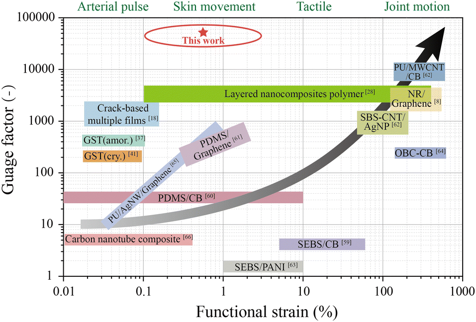 | ||
| Fig. 6 A comparison of gauge factor and functional strain with other materials.8,18,28,37,41,59–66 | ||
4. Experimental
Preparation
Pure chromium, germanium, and tellurium targets were used with the radiofrequency magnetron sputtering method to deposit CrGT films on polyimide substrates. The as-deposited amorphous phase can be transformed into a c-axis oriented crystalline phase after annealing at 360 °C. X-ray diffraction (XRD) and energy-dispersive X-ray spectroscopy (EDX) were used to ensure that the CrGT films comprised a single phase with the correct quantitative ratio of Ge:Cr:Te = 24.2 at%:17.3 at%:59.5 at%.
Tensile test
The tensile test was conducted by using an in situ material testing system (Sanko ISL-S500) with a resolution of 1 nm. Foil samples with dimensions of 5 mm × 20 mm were used to evaluate the piezoresistive performance, and the electrode distance was set to 10 mm. The tensile displacement speed was set to 0.5 mm s−1, and the sampling interval was set to 50 ns.Vibration experiment
The DYN-MS-100 Shaker (DynaLabs) was used to provide dynamic force excitation in the cantilever vibration experiment. The shaker includes a sine frequency generator, so the frequency and amplitude can be controlled directly. However, owing to the limitation of maximum acceleration, the amplitude decreased with increasing frequency except when resonance occurred.Finite element analysis
FEA was performed by using the Ansys Mechanical Enterprise package. The in-plane size of the sample was the same as in the experiment at 10 mm × 5 mm. The polyimide and CrGT films were 25 μm and 100 nm thick, respectively. A three-dimensional geometric model was built and meshed into 5600 elements, which was defined as the finest 3D 20-node coupled-field solid type. As boundary conditions, the displacements in three directions of the center point were restricted to zero. External displacements were evenly applied to two edges in the width direction to simulate the tensile deformation process.Characterization
Scanning electron microscopy/energy-dispersive X-ray spectroscopy
The surface morphology after the tensile test was observed by scanning electron microscopy (JEOL JSM-6500F), for which all samples were carbon coated.Laser microscopy
In situ surface observation of the samples during the tensile test was conducted by using laser microscopy (Lasertec OPTELICS HYBRID+ MC2000). The tensile test machine was set just beneath the lens, and the surface morphology, and distance change between two lines drawn by a marker in advance were observed.X-ray diffraction
XRD spectra were measured at room temperature with a Cu Kα source using conventional 2θ/θ Bragg–Brentano geometry (Rigaku, ULTIMA).Resistance measurement
The resistance change was measured by using an electrometer (KEYSIGHT B2985B) and semiconductor parameter analyzer (Agilent 4155C).Data availability
The authors declare that the data supporting the findings of this study are available within the paper.Conflicts of interest
There are no conflicts to declare.Acknowledgements
This work was supported by JSPS KAKENHI (grant no. 21H05009, 22KJ0244, 23K17825).Notes and references
- G. Chen, X. Xiao, X. Zhao, T. Tat, M. Bick and J. Chen, Chem. Rev., 2022, 122, 3259 CrossRef CAS PubMed
.
- L. Wang, Z. Lou, K. Jiang and G. Shen, Adv. Intell. Syst., 2019, 1, 1900040 CrossRef
- S. M. A. Iqbal, I. Mahgoub, E. Du, M. A. Leavitt and W. Asghar, npj Flexible Electron., 2021, 5, 9 CrossRef
- Y. Wang, Y. Yu, X. Wei and F. Narita, Adv. Mater. Technol., 2022, 7, 2200318 CrossRef
- J. Liu, H. Wang, T. Liu, Q. Wu, Y. Ding, R. Ou, C. Guo, Z. Liu and Q. Wang, Adv. Funct. Mater., 2022, 32, 2204686 CrossRef CAS
- J. Gao, Y. Fan, Q. Zhang, L. Luo, X. Hu, Y. Li, J. Song, H. Jiang, X. Gao, L. Zheng, W. Zhao, Z. Wang, W. Ai, Y. Wei, Q. Lu, M. Xu, Y. Wang, W. Song, X. Wang and W. Huang, Adv. Mater., 2022, 34, 2107511 CrossRef CAS PubMed
- J. He, Y. Zhang, R. Zhou, L. Meng, C. Pan, W. Mai and T. Chen, J. Materiomics, 2020, 6, 86 CrossRef
- C. S. Boland, U. Khan, C. Backes, A. O’Neill, J. McCauley, S. Duane, R. Shanker, Y. Liu, I. Jurewicz, A. B. Dalton and J. N. Coleman, ACS Nano, 2014, 8, 8819 CrossRef CAS PubMed
- Y. R. Jeong, H. Park, S. W. Jin, S. Y. Hong, S. S. Lee and J. S. Ha, Adv. Funct. Mater., 2015, 25, 4228 CrossRef CAS
- Z. Liu, D. Qi, P. Guo, Y. Liu, B. Zhu, H. Yang, Y. Liu, B. Li, C. Zhang, J. Yu, B. Liedberg and X. Chen, Adv. Mater., 2015, 27, 6230 CrossRef CAS PubMed
- M. Amjadi, K. U. Kyung, I. Park and M. Sitti, Adv. Funct. Mater., 2016, 26, 1678 CrossRef CAS
- Q. Zheng, J. Lee, X. Shen, X. Chen and J. K. Kim, Mater. Today, 2020, 36, 158 CrossRef CAS
- D. Lei, N. Liu, T. Su, Q. Zhang, L. Wang, Z. Ren and Y. Gao, Adv. Mater., 2022, 34, 2110608 CrossRef CAS PubMed
- L. Guo, S. Hu, X. Gu, R. Zhang, K. Wang, W. Yan and X. Sun, Adv. Mater., 2023, 2301854 Search PubMed
- V. Zardetto, T. Brown, A. Reale and A. Di Carlo, J. Polym. Sci., Part B: Polym. Phys., 2011, 49, 638 CrossRef CAS
- M. Hassan, G. Abbas, N. Li, A. Afzal, Z. Haider, S. Ahmed, X. Xu, C. Pan and Z. Peng, Adv. Mater. Technol., 2022, 7, 2100773 CrossRef
- Y. Kim, J. Lee and S. K. Kang, J. Mech. Sci. Tech., 2022, 36, 1059 CrossRef
- T. Lee, Y. W. Choi, G. Lee, S. M. Kim, D. Kang and M. Choi, RSC Adv., 2017, 7, 34810 RSC
- M. Abshirini, M. C. Saha, M. C. Altan and Y. Liu, Adv. Mater. Technol., 2022, 7, 2101555 CrossRef CAS
- Y. Gao, C. Yan, H. Huang, T. Yang, G. Tian, D. Xiong, N. Chen, X. Chu, S. Zhong, W. Deng, Y. Fang and W. Yang, Adv. Funct. Mater., 2020, 30, 1909603 CrossRef CAS
- L. Singh, k Tripathy and M. Bhattacharjee, Adv. Eng. Mater., 2022, 24, 2200500 CrossRef CAS
- C. M. Wang, C. H. Hsieh and W. S. Liao, Adv. Mater. Interfaces, 2020, 7, 1902202 CrossRef CAS
- H. Chang, S. Kim, T. H. Kang, S. W. Lee, G. T. Yang, K. Y. Lee and H. Yi, ACS Appl. Mater. Interfaces, 2019, 11, 32291 CrossRef CAS PubMed
- J. C. Yang, J. Mun, S. Y. Kwon, S. Park, Z. Bao and S. Park, Adv. Mater., 2019, 31, 1904765 CrossRef CAS PubMed
- B. Pang, Z. Jin, Y. Zhang, Z. Liu, W. She, P. Wang, Y. Yu, X. Zhang, C. Xiong, N. Li, G. Sun, P. Zhao, G. Liu, X. Song and S. Gao, Adv. Funct. Mater., 2022, 32, 2208676 CrossRef CAS
- M. Ha, S. Lim, J. Park, D. S. Um, Y. Lee, H. Ko, M. Ha, S. Lim, J. Park, D. Um, Y. Lee and H. Ko, Adv. Funct. Mater., 2015, 25, 2841 CrossRef CAS
- G. Yang, Y. Yang, T. Chen, J. Wang, L. Ma and S. Yang, ACS Appl. Nano Mater., 2022, 5, 1068 CrossRef CAS
- Y. Wang, R. Shu and X. Zhang, Angew. Chem., Int. Ed., 2023, 62, e202303446 CrossRef CAS PubMed
- J. Zhang, B. Xu, K. Chen, Y. Li, G. Li and Z. Liu, SusMat, 2024, e207 CrossRef CAS
- Y. H. Wu, H. Z. Liu, S. Chen, X. C. Dong, P. P. Wang, S. Q. Liu, Y. Lin, Y. Wei and L. Liu, ACS Appl. Mater. Interfaces, 2017, 9, 20098 CrossRef CAS PubMed
- J. Tong, N. Wang, Q. Wang, S. Chen, B. Sheng, S. X. Yue and L. Hui, Sens. Actuators, B, 2022, 358, 131497 CrossRef CAS
- Y. Wang, F. Wang, S. Yazigi, D. Zhang, X. Gui, Y. Qi, J. Zhong and L. Sun, Carbon, 2022, 173, 849 CrossRef
- C. Zhang, J. Sun, Y. Lu and J. Liu, J. Mater. Chem. C, 2021, 9, 754 RSC
- T. Yang, X. Li, X. Jiang, S. Lin, J. Lao, J. Shi, Z. Zhen, Z. Li and H. Zhu, Mater. Horiz., 2016, 3, 248 RSC
- J. Kim, Y. Lee, M. Kang, L. Hu, S. Zhao and J. H. Ahn, Adv. Mater., 2021, 33, 2005858 CrossRef CAS PubMed
- D. J. Liaw, K. L. Wang, Y. C. Huang, K. R. Lee, J. Y. Lai and C. S. Ha, Prog. Polym. Sci., 2012, 37, 907 CrossRef CAS
- Z. Wang, C. Dong, X. Wang, M. Li, T. Nan, X. Liang, H. Chen, Y. Wei and H. Zhou, npj Flexible Electron., 2018, 2, 17 CrossRef
- N. Yamada, E. Ohno, K. Nishiuchi, N. Akahira and M. Takao, J. Appl. Phys., 1991, 69, 2849 CrossRef CAS
- S. Shindo, Y. Sutou, J. Koike, Y. Saito and Y. H. Song, Mater. Sci. Semicond. Process., 2016, 47, 1 CrossRef CAS
- E. Mazhnik and A. R. Oganov, A Model of Hardness and Fracture Toughness of Solids, J. Appl. Phys., 2019, 126, 125109 CrossRef
- F. F. Schlich, A. Wyss, H. Galinski and R. Spolenak, Acta Mater., 2017, 126, 264 CrossRef CAS
- S. Hatayama, Y. Shuang, P. Fons, Y. Saito, A. V. Kolobov, K. Kobayashi, S. Shindo, D. Ando and Y. Sutou, ACS Appl. Mater. Interfaces, 2019, 11, 43320 CrossRef CAS PubMed
- S. Hatayama, Y. Sutou, S. Shindo, Y. Saito, Y. H. Song, D. Ando and J. Koike, ACS Appl. Mater. Interfaces, 2018, 10, 2725 CrossRef CAS PubMed
- A. A. Barlian, W. T. Park, J. R. Mallon, A. J. Rastegar and B. L. Pruitt, Proc. IEEE, 2009, 97, 513 CAS
- C. S. Smith, Phys. Rev., 1954, 94, 1295 Search PubMed
- W. P. Mason and R. N. Thurston, J. Acoust. Soc. Am., 1957, 29, 1096 CrossRef
- H. Hu, Z. Wang, Y. Luo, P. Wang, Y. Zhang, Q. Huang and Z. Zheng, Thin Solid Films, 2023, 779, 139920 CrossRef CAS
- N. Kyokuta, M. Koba, T. Araki, S. Nambu, J. Inoue and T. Koseki, J. Jpn. Inst. Metals, 2012, 76, 272 CrossRef CAS
- R. A. Meirom, T. E. Clark and C. L. Muhlstein, Acta Mater., 2012, 60, 1408 CrossRef CAS
- J. Riedle, P. Gumbsch and H. F. Fischmeister, Phys. Rev. Lett., 1996, 76, 3594 CrossRef CAS PubMed
- P. Lemaitre, J. Mater. Sci. Lett., 1988, 7, 896 Search PubMed
- R. G. Munro, S. W. Freiman and T. L. Baker, NIST IR, 1998, p. 6153.
- R. E. Jones, J. M. Rimsza and L. J. Criscenti, J. Phys.: Condens. Matter, 2018, 30, 245901 CrossRef CAS PubMed
- E. Vernaz, F. Larche and J. Zarzycki, J. Non-Cryst. Solids, 1980, 37, 359 CrossRef CAS
- J. Ross, E. H. Sonnenblick, J. W. Covell, G. A. Kaiser and D. Spiro, Circ. Res., 1967, 21, 409 CrossRef PubMed
- W. B. Kannel, F. T. Gordon and M. J. Schwartz, Am. J. Cardiol., 1971, 27, 335 CrossRef CAS PubMed
- Z. Zhang, Z. Pi and B. Liu, IEEE Trans. Biomed. Eng., 2015, 62, 522 Search PubMed
- D. Castaneda, A. Esparza, M. Ghamari, C. Soltanpur and H. Nazeran, Int. J. Biosens. Bioelectron., 2018, 4, 195 Search PubMed
- M. Melnykowycz, M. Tschudin and F. Clemens, Sensors, 2016, 16, 326 CrossRef PubMed
- Y. Zheng, Y. Li, Z. Li, Y. Wang, K. Dai, G. Zheng, C. Liu and C. Shen, Compos. Sci. Technol., 2017, 139, 64 CrossRef CAS
- X. Li, T. Yang, Y. Yang, J. Zhu, L. Li, F. E. Alam, X. Li, K. Wang, H. Cheng, C. Lin, Y. Fang and H. Zhu, Adv. Funct. Mater., 2016, 26, 1322 CrossRef CAS
- S. Zhao, J. Li, D. Cao, Y. Gao, W. Huang, G. Zhang, R. Sun and C. Wong, J. Mater. Chem. C, 2016, 4, 6666 RSC
- P. Costa, J. Oliveira, L. Horta-Romarís, M. Abad, J. A. Moreira, I. Zapiráin, M. Aguado, S. Galván and S. Lanceros-Mendez, Compos. Sci. Technol., 2018, 168, 353 CrossRef CAS
- L. Duan, D. R. D’hooge, M. Spoerk, P. Cornillie and L. Cardon, ACS Appl. Mater. Interfaces, 2018, 10, 22678 CrossRef CAS PubMed
- S. Chen, Y. Wei, S. Wei, Y. Lin and L. Liu, ACS Appl. Mater. Interfaces, 2016, 8, 25563 CrossRef CAS PubMed
- M. Li, J. Wang, S. Wang, T. Zuo, W. Sun, Y. Gu and Z. Zhang, Mater. Res. Express, 2019, 6, 025034 CrossRef
| This journal is © The Royal Society of Chemistry 2024 |