
 Open Access Article
 This Open Access Article is licensed under a Creative Commons Attribution-Non Commercial 3.0 Unported Licence
Ultrawide linear range, high sensitivity, and large-area pressure sensor arrays enabled by pneumatic spraying broccoli-like microstructures†
Zonglin
Li
abc,
Kun
Li
abc,
Weiwei
Wang
abc,
Tong
Zhang
 *abd and
Xiaoniu
Yang
*abc
*abd and
Xiaoniu
Yang
*abc
aState Key Laboratory of Polymer Physics and Chemistry, Changchun Institute of Applied Chemistry, Chinese Academy of Sciences, Changchun 130022, China. E-mail: tzhang@ciac.ac.cn; xnyang@ciac.ac.cn
bSchool of Applied Chemistry and Engineering, University of Science and Technology of China, Hefei, 230026, China
cCAS Key Laboratory of High-Performance Synthetic Rubber and its Composite Materials, Changchun Institute of Applied Chemistry, Chinese Academy of Sciences, Changchun 130022, China
dHuangpu Institute of Materials, Changchun Institute of Applied Chemistry, Chinese Academy of Science, Guangzhou 510530, China
First published on 1st March 2024
Abstract
Large-area pressure sensor arrays with a wide linear response range and high sensitivity are beneficial to map the inhomogeneous interface pressure, which is significant in practical applications. Here, we demonstrate a pneumatic spraying method to prepare large-area microstructure films (PSMF) for high performance pressure sensor arrays. The sprayed surface morphology is designable by controlling the spraying parameters. It is worth noting that the constructed “broccoli” like morphology with a swollen top and shrunken bottom inspired a new mechanism to enlarge the linear response range by decreasing the series resistance with pressure increasing. At the same time, the pneumatic sprayed “broccoli” has a rough surface due to droplet stacking, which reduces the initial current effectively. Hence, the sensor achieves a 10![[thin space (1/6-em)]](https://www.rsc.org/images/entities/char_2009.gif) 000 kPa ultrawide linear response range with a high sensitivity (98.71 kPa−1), and low detection (5 Pa). The prepared sensor has a small static response error (4.4%) and 5000 cycle full-range dynamic response durability. Finally, the constructed sensor arrays can distinguish the pressure distribution in different ranges clearly, which indicates a great potential in health care, motion detection, and the tire industry.
000 kPa ultrawide linear response range with a high sensitivity (98.71 kPa−1), and low detection (5 Pa). The prepared sensor has a small static response error (4.4%) and 5000 cycle full-range dynamic response durability. Finally, the constructed sensor arrays can distinguish the pressure distribution in different ranges clearly, which indicates a great potential in health care, motion detection, and the tire industry.
New conceptsAt present, transfer is a conventional method to obtain microstructure films used in piezoresistive pressure sensors, but has drawbacks such as the difficulty of large-area preparation, and it being expensive. Meanwhile, the lack of new microstructure morphologies has limited the further improvement of sensor performance in sensitivity and linear response range. Here, we have demonstrated a new strategy to construct large-area, high-performance flexible pressure sensor arrays by pneumatic spraying microstructure films (PSMF). The sprayed microstructure is designable by adjusting the spraying parameters. One of the unique sprayed morphologies has a broccoli-like profile (PSMF-B) which inspired a new conducting mechanism that the series resistance varies with pressure. A large-area PSFM (60 × 60 cm2) is fabricated, and the prepared pressure sensor has an ultra-wide linear range (10000 kPa) and high sensitivity (98.71 kPa−1). Since the microstructures also play an important role in pressure sensors based on piezo capacitance or a triboelectric nanogenerator, we believe that the underestimated pneumatic spraying might bring new findings in these fields.
|
Introduction
High performance, large-area flexible presser sensor (FPS) arrays have shown great potential in electronic skins,1–3 healthcare systems,4 and human machine interfaces.5,6 The working principle of FPSs can be roughly classified into piezoresistive,7–9 capacitance,1,10–12 piezoelectric,13,14 and triboelectric.15,16 Among these, piezoresistive pressure sensors based on surface microstructures that can convert the external force stimuli into a contact resistance change have been widely investigated due to their simple structure, convenient signal readout, temperature insensitivity, and fast response.5,9Linear range and sensitivity are two core parameters to evaluate an FPS, which researchers are striving to improve.8 A wider linear range enables FPSs to fulfil the requirements beyond daily life in harsh environments,17 and makes the signal post-processing convenient,11 while a higher sensitivity is required when monitoring faint human-body-induced deformations or mimicking human skin.18 However, there is a trade-off between the two parameters that a wider linear range corresponds to a lower sensitivity and vice versa.19,20 This is because the high apparent modulus microstructure has to prevent the saturation of the contact area in the high pressure range, but the sensing of tiny force is unavoidably neglected. To solve this dilemma, lots of regular/irregular multi-level/hierarchical microstructures have been transferred from various moulds, such as patterned silicon chips,21,22 sandpaper,2,8 leaves,23 silk,24 selective laser sintering surfaces,25etc. The elaborately designed microstructures will effectively reduce the initial contact area and mobilize the deformation under high pressure, which can partly solve the problem.26
However, the lack of new morphologies has limited the further promotion of FPS performance. Meanwhile, it can be hard to construct a uniform large-area microstructure film by transfer due to the difficulty of levelling or demoulding. Cost wise, the manufacture of moulds, and the raw material (polydimethylsiloxane, commonly) are both expensive.27 Therefore, developing a non-transfer, low-cost, large-area microstructure film preparation method for high performance flexible pressure sensor arrays is imperative. Jia et al.17 fabricated a piezoresistive flexible pressure sensor based on electrospinning polyimide textile, which has a wide range response (from Pa to MPa), and the ability to serve in harsh environments. The authors showed large-area fibre fabrics (1 × 1.5 m2) with various thicknesses, which will be conducive to improving the large-area preparation efficiency. Jung et al.5 constructed hierarchical random microstructures by thermal expansion of microspheres in elastic substrates. Their work shows potential in large-area preparation and the fabricated sensor has a high sensitivity (−50.45 kPa−1). Although researches have confirmed several feasible and efficient approaches for large-area microstructure film preparation, the trade-off between linear range and sensitivity is still unresolved.
Herein, a convenient one-step pneumatic spraying method is employed to construct large-area, high-performance, uniform microstructure films for the first time (Fig. 1). Three unreported morphologies have been constructed by adjusting the spraying parameters. The variable series resistance (VSR) conduction mechanism, which only appears in the swollen top and small bottom Broccoli-like microstructure (PSMF-B), has effectively enlarged the response linearity in an ultrawide pressure range. Otherwise, when spraying, the random stacking of droplets leads to an extremely rough and irregular surface, which significantly reduces the initial contact area and brings a vast improvement in sensitivity. As a consequence, a record-breaking 10000 kPa ultrawide linear range and 98.71 kPa−1 high sensitivity is accomplished by the PSMF-B type pressure sensor. This work explored a feasible method to prepare large-area microstructure films. The designable spraying morphology indicates potential in new conduction mechanism discovery, which may promote the sensor performance and boost the development of FPSs further.
 | ||
| Fig. 1 Overview of the large-area sensor array based on PSMF. (a-i) Schematic of the PSMF mechanism; (a-ii) a PSMF of about 60 × 60 cm2 large-area; (a-iii) height uniformity of the constructed PSMF. (b-i) Sensor array for pressure distribution detection; (b-ii) schematic diagram of a single sensing unit structure; (b-iii) correspondence of sensor output and input. (c) Diversified applications under different pressure ranges that the fabricated sensor is qualified. | ||
Results and discussion
Design and fabrication of the PSMF
Pneumatic spraying is generally used in industry to construct large-area coatings. Sometimes, the coating surface is not smooth enough for various reasons, and this inspired a one-step method to fabricate microstructures instead. A spray coating microstructured surface has been utilized to prepare superhydrophobic and superoleophobic surfaces,28 but application in FPSs has not been reported yet. Fig. 1a-i illustrates the theoretical atomization and deposition process when spraying. First, the solution will flow out at the nozzle and form a liquid film. Then, the compressed gas will blow through the surface of the liquid film at a high speed causing unstable fluctuations and tongues. Under the force of gas turbulence, the tongues break into large droplets (first broken). These droplets continue to be affected by gas turbulence during the flight. If the viscosity and surface tension of the liquid is not enough to resist the external force, the droplets will continue to break up and become tiny droplets (second broken).29 The microstructure is eventually obtained on the substrate after repeated stacking and drying of droplets. The formation process of pneumatic spraying microstructures is systematically investigated in Fig. S1 (ESI†). A 60 × 60 cm2 PSMF is successfully prepared by a self-built three axis automatic spraying device, as shown in Fig. 1a-ii and Movie S1 (ESI†). The uniformity of a 30 × 30 cm2 large-area PSMF was evaluated by measuring the arithmetic mean height (σSa), which contains 16 sampling areas (24 × 18 mm2 for each) (Fig. S2, ESI†). The similar height and concentrated height distribution indicate a great height uniformity all over the surface (Fig. 1a-iii and Fig. S2, ESI†). The pressure mapping of the contact interface, which provides a wealth of useful information, must be conducted on a sensor array (Fig. 1b-i).30 For a single sensing unit in a sensor array, a widely used device structure is exhibited in Fig. 1b-ii, which is also adopted in this work. The simple device only needs to encapsulate a surface conductive microstructure film and an interdigital face-to-face. When applying varying load, the contact area between the conductive surface and interdigital electrode (IDE) will change accordingly, so the response current also changes (Fig. 1b-iii). Due to the outstanding performance, the prepared sensors and sensor arrays are competent in radial artery pulse monitoring (∼10 kPa), plantar pressure detection (∼100 kPa), and tire impression analysis (∼1000 kPa)20,31 (Fig. 1c).Morphological characteristics
At present, transfer printing is a general approach to obtain microstructure films. However, the morphologies of the transferred microstructures are similar since most of the available moulds have been explored. As a consequence, the lack of new morphology limits the further improvement of the sensor performance. In this work, three kinds of spray-coated novel microstructures with porous internal structures and complex surfaces are shown in Fig. 2a and Fig. S3 (ESI†). Specifically, when the solution concentration is 20 mg mL−1, sprayed droplets agglomerate into different size particles distributed on the substrate surface randomly and uniformly. Most large particles have a swollen top, and little bottom profile. From the top view, each particle is composed of multiple blades irregularly, and smaller particles are scattered at the edge of the blades forming a multilevel structure. Due to its similar profile to “Broccoli”, this unique shape is named PSMF-B. To our best knowledge, this is the first time that this inverse pyramid-like microstructure has been employed in FPS. When the concentration is 50 mg mL−1, the pneumatic spraying microstructure has an undulating surface and porous interior. From the top view, the film shows a network surface with small liquid films and grains on it. This morphology is named PMSF-M (M for “Mountain”). As the solution becomes thicker (80 mg mL−1), the PSMF presents a “Textile” like appearance (PMSF-T) which has a crisscross fibrous interior with a large liquid film and droplet grains on the flat surface. The 3D numerical profiles of PSMF are also constructed by a 3D profilometer to discover the differences statistically (Fig. 2b). As the height variation along specific lines (BB′, MM′, and TT′) listed below, both BB′ and MM′ have a similar height drop (BB′ 355 μm, MM′ 336 μm) and TT′ has a flatter surface with a maximum drop of 63 μm. However, BB′ has more ups and downs in the same length, which means that PSMF-B has a higher protuberant structure density than PSMF-M. The height distribution of a certain area (7.56 × 5.67 mm2) contains 1280 × 768 points height data as shown in Fig. 2c. PSMF-B has a wider distribution corresponding to its multi-level surface. More numerical surface features and morphology parameters are shown in Table S1 (ESI†). | ||
| Fig. 2 Morphological characteristics of PSMFs. (a) SEM images of PSMFs on the view of side, and top. (b) 3D surface profile measurement results of the PSMFs (7.56 mm × 5.67 mm) and height of the specific lines. (c) Height distribution of PSMFs (7.56 mm × 5.67 mm). | ||
Sensing characterization of PSMF sensors
The performance of a single pressure sensor was measured by a system depicted in Fig. 3a. Flexible pressure sensors based on PSMF were powered and recorded by a source measure unit, while the load was applied by a universal test machine equipped with a reference pressure sensor. In Fig. 3b, PSMF sensors under various loads have straight and equiangular transformed lines which indicates that the sensor has an ohmic contact resistance. Fig. 3c shows that the prepared sensor can respond to different pressures stably. In short, these basic tests have proved that the fabricated devices based on PSMF are able to transduce variable loadings into current responses.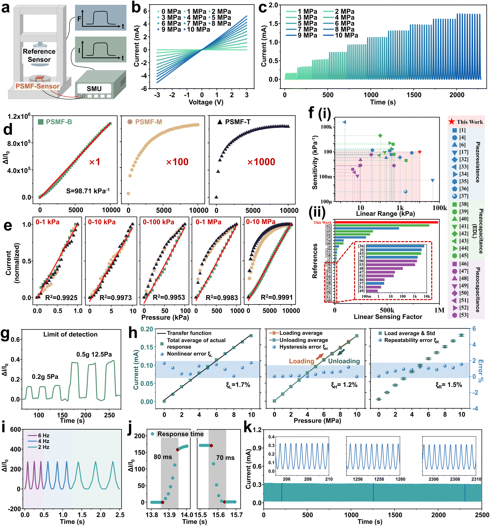 | ||
| Fig. 3 Sensing performance of flexible pressure sensors based on PSMF. (a) Schematic diagram of the testing device. (b) Sweep voltage test under different pressures. (c) Ten times loading cycle test under different pressures. (d) Relative current variation of the sensors based on PSMF-B, PSMF-M, and PSMF-T under various pressures from 0 to 10000 kPa. (e) The normalized pressure-current relation of the sensors based on PSMF in the pressure range of 0–1, 0–10, 0–100, 0–1000, and 0–10000 kPa. (f) Comparison of this work with reported piezoresistive, piezocapacitive, and piezocapacitive (EDL) flexible pressure sensors in the prospect of linearity range and sensitivity. (g) Limit of detection. (h) Errors of the sensor, including nonlinear error ξL, hysteresis error ξH, and repeatability error ξR. (i) Frequency response. (j) Response time. (k) 5000 cycles of full-scale fatigue testing. | ||
More detailed tests were carried out on 2 × 2 cm2 flexible PSMF sensors whose object picture is shown in Fig. S4 (ESI†). Fig. 3d plots the relationship between the loading pressure and relative current (ΔI/I0) of the sensors. Due to the largest Spc (Table S1, ESI†), PSMF-B has the minimum initial contact area and the minimum initial current (I0), resulting in a much higher relative current change. Since the relative current change of PSMFs is on different orders of magnitude, the values of PSMF-M, and PSMF-T are multiplied by 100, and 1000 times, respectively, for the intuitive comparison with PSMF-B. The sensitivity is commonly defined as S = (ΔI/I0)/P. It is worth noticing that PSMF-B shows excellent linearity (R2 = 0.9991) in the 10000 kPa whole range with a high sensitivity (98.71 kPa−1). By contrast, the response of the sensors based on PSMF-M and PSMF-T is saturated quickly. To inspect the responsiveness of the three morphologies in different pressure ranges, the normalized outputs are plotted, as shown in Fig. 3e. In a lower pressure (≤ 10 kPa) range, PSMF-M and PSMF-T show quite a linearity response like PSMF-B. When the pressure range increases, PSMF-M and PSMF-T get nonlinear while PSMF-B keeps good linearity in the whole range (R2 > 0.99). In Fig. 3f–i and Table S2 (ESI†), the high performance PSMF-B pressure sensor is compared favourably with the reported literature, including piezoresistive, piezocapacitance, and piezocapacitance, which employed an electric double layer (EDL).1,4,6,17,32–53 The trade-off between response range and sensitivity can be balanced by regulating the elastic modulus.1,25,54 Therefore, the product of the linear range and the sensitivity (linear sensing factor)55 can reflect the sensors performance without the influence of material moduli difference. As is depicted in Fig. 3f-ii, FPS based on PSMF-B has the largest enclosed area which means the best comprehensive performance. The reason of the breaking-record property will be discussed in the following from the contact area, conduction path, and simulation perspectives.
 | ||
| Fig. 4 The mechanism of the outstanding performance of sensors based on PSMF-B. (a) The contact area between interdigital electrodes (IDE) and microstructure surface enlarged when the loading is increased. (b) Schematic of the current path between adjacent IDEs. (c) In situ pressure-contact area observation device. (d) Maps of contact region under various pressures of PSMF and plots of the contact area versus applied pressure. (e) Rc and 1/Rc considered the total contact area. (f) Schematic of the Rsv test and corresponding data. (g) Schematic of the Rsh test and corresponding data. (h) Schematic of the current path in PSMF-B. (i) The normalized current response of the PSMF sensors in the theoretical model and in situ testing. | ||
Static performances of the PSMF-B pressure sensors are shown in Fig. 3g and h. The ability to perceive tiny pressure is meaningful to electronic skins.56 Here, the sensor shows a low detection limit of 5 Pa (0.2 g) and 12.5 Pa (0.5 g) with certain repeatability (Fig. 3g). The total error of a sensor contains nonlinear error ξL, hysteresis error ξH, and repeatability error ξR. The nonlinear error reflects the deviation degree of the actual tested response points from the fitting line (transfer function). The hysteresis error is the inconsistence in response of a certain pressure when loading and unloading. The repeatability error is the inconsistence of the outputs when loading at the same pressure many times. In this work, the total error is controlled at 4.4% and the three types of errors are 1.7%, 1.2%, and 1.5%, respectively (Fig. 3h), which indicates a high-precision perception (the original data of repeatability error test is supplemented in Table S3, ESI†). The calculation of errors can be found in Note S1 (ESI†). Dynamic performances are shown in Fig. 3i–k. In Fig. 3i, the ΔI/I0-t curve shows that the sensor responds to the different loading frequencies stably. The sensor with the “broccoli” like microstructure also exhibits a quite fast response/recovery of 80/70 ms from a loading of 75 kPa (Fig. 3j). In Fig. 3k, the maximum response of the PSMF-B sensor after 5000 cycles full range (100–10000 kPa) fatigue test decays 4.7% (from 0.3229 to 0.3083 mA), indicating an excellent durability. Fig. S5 (ESI†) shows the PSMF-B sensor durability in lower ranges as 10–100 kPa and 100–1000 kPa, which are also pretty stable.
Sensing mechanism of the ultrawide linear range
As depicted in Fig. 4a, the fundamental basis of surface microstructure FPS sensing is the expansion of the contact area (red shaded) when pressing. For the simplified circuit model, the total resistance of an FPS contains a variable contact resistance (Rc) and a series resistance (Rs) of the uncontacted area. For a better understanding of the sensor performance, in Fig. 4b, the Rs is further divided into a vertical component (Rsv), which exists on the surface of the raised microstructure, and a horizontal component (Rsh) that lies on the flattened substrate. Thus, the total resistance (Rt) is depicted as Rt = Rc + Rsv + Rsh. So, the relationship of the applied pressure and real contact area will reveal the Rc variation principle, which is indispensable to explain the brilliant performance of PSMF-B sensors. A morphology-electricity in situ test device is developed for this purpose, as shown in Fig. 4c. The activated PSMF sensor is placed on the reference pressure sensor. As the reference pressure sensor is lifted by a lifting table, the PSMF sensor will be pressed on the transparent observation window. Then, the contact image, response current, and applied pressure can be obtained simultaneously. Fig. 4d maps the evolution of the PSMF contacted area under increasing loading from 200 kPa to 10400 kPa (represented by different colours). The original images captured by optical microscope are shown in Fig. S6 (ESI†), where the golden area is the contacted region of the PSMF-B and indium tin oxide (ITO)@PET interdigital electrode. As plotted below, the maximum effective contact area identified from the in situ observation all accounts for about 70% of the total pressed which is mainly benefiting from the easily compressed internal porous structure. Otherwise, as the applied pressure gets higher, the contact region of PSMF-B keeps increasing in the whole range while PSMF-M exhibits saturation at around 5 MPa, and PSMF-T is saturated at 3 MPa. The reason can be deduced by the morphology that PSMF-B has the widest surface height distribution range (Fig. 2c), and the biggest corresponding maximum height of the surface (Sz) (Table S1, ESI†). This multi-level morphology enables new contacts to continuously emerge with increasing pressure. However, since the Rc of a constant area also decreases with pressing (Fig. S7, ESI†), the difference between PSMF is then eliminated when considering that the overall Rc is inversely proportional to the contact area (Fig. 4e). Generally, if Rc varies in the same fashion, the responses of the sensors should have the same trend because Rs is a constant in most situations. However, the decreased Rs of PSMF-B breaks this common sense. The Rsv test was conducted by pressing a fixed exposing area (∼1.5 mm2) ITO@glass electrode on microstructure surfaces (Fig. 4f and Fig. S8, S9, ESI†). The Rsh test was conducted on a 1 × 1.5 cm2 microstructure film with electrodes connected to the two short edges, respectively (Fig. 4g). In both situations, resistance in PSMF-B declines with increasing loading following a negative power law. Combining the previous morphological characterization, a novel conductive model of PSMF-B is proposed, as depicted in Fig. 4h. For the big top and small bottom configuration, it is obvious that the surface will self-contact due to compression. Thus, a reduced resistance appears no matter whether the current flows vertically (Rsv) or horizontally (Rsh). Fig. 4i shows that the current calculated by the simplified model has the same trend as the current measured in situ, which indicates that the assumed model is close to the real one (for more details refer to Note S2, ESI†).
Applications of the large-area pressure sensing array and single sensors
Profiting from the convenience of the fabrication method and unique morphology, the prepared PSMFs are ease to be processed into sensor arrays and show great potential in full range application scenarios. Fig. 5a exhibits the components of a pressure distribution detection system. The device is composed of a sensing array which contains 4096 units, a flat cable, and a signal processing unit. The sensing array is fabricated by laser-etching of a surface conductive PSMF into grids, then assembled with an IDE array in a face-to-face manner. Sensor arrays that appear below in different sizes are prepared based on PSMF-B. In the low pressure range, pulse mapping for pulse diagnosis is extensively noticeable at present.57Fig. 5c-i shows 12 channel pulse monitoring data that may assist traditional Chinese medicine by revealing the pulse patterns of Cun, Guan, Chi, and Lower Chi. Fig. 5c-ii shows the enlarged waveform of the Chen pulse in channel-8, which is pretty clear to distinguish the three crests. In the post pandemic era, face masks have become a regular item in daily life to prevent various respiratory infectious diseases and reduce the damage of inhalable particulate matter to the lungs. Therefore, a smart mask is convenient and beneficial for personal health care.16 As is shown in Fig. 5d, a disposable medical surgical masks attached with the fabricated sensor were worn on a volunteer's face. The clear respiratory waveform indicates that the sensor is sensitive to small vibrations, which has potential to be applied in the field of respiratory monitoring. The large-area sensor array also shows prominent prospective in medium pressure, human activity detection, such as sports, and health care fields.58 As shown in Fig. 5e, when a foot steps on a circle sensing pad with 30 cm diameter, the pressure distribution image is clearly displayed. In Fig. 5f, a complex but reasonable wave is produced by a single sensor attached on the forefoot when the volunteer is jumping (detailed interpretation for the waveform is shown in Fig. S10, ESI†). In the tire industry, a high-pressure sensing pad is needed to acquire the impression, which is of great significance to the material and pattern design. A high-density sensing array containing 64 × 64 units (2 × 1.7 mm2 for each unit) was placed on a metal flat plate then pressed by a tire as illustrated in Fig. 5g-i. As the load increases, the contact area enlarges while the three main drainage ditches are still unclosed (Fig. 5g-ii). The performance uniformity of different sensor array units was also evaluated as shown in Fig. S11 (ESI†). The relative standard deviation (RSD) is 28.2% (@254.8 kPa) which indicates a pretty good uniformity. These tests have exhibited the potential of PSMF in large-area, various range pressure high quality detection. | ||
| Fig. 5 Applications of flexible pressure sensing arrays and a single sensor in various pressure ranges. (a) Optical photo of a pressure distribution detection system with 4096 sensing units. (b) Microstructure array and IDE array. Low pressure test: (c-i) pulse detection with a 12-pixel array; (c-ii) enlarged waveform of channel-8; (d) respiration monitoring. Medium pressure test: (e) plantar pressure distribution test; (f) variation of forefoot pressure when jumping. High pressure test: (g-i) optical image of the tire impression test; (g-ii) corresponding results. | ||
Conclusions
In conclusion, this paper demonstrates a convenient, large-area microstructure elastic film preparation method for flexible pressure sensors arrays based on pneumatic spraying. The designable morphologies provide insights into the novel mechanism and excellent performance. As a proof of concept, PSMF-B, M, and T are fabricated and implemented in sensors. Among them, PSMF-B with an enlarged top and a small bottom provides a new perspective that the decreasing series resistance during compression could expand the sensing range (10000 kPa). Meanwhile, the sharp tips of “broccolis” also reduce the initial contact area, corresponding to a smaller initial current and higher sensitivity (98.71 kPa−1). In terms of application, large-area PSMF (60 × 60 cm2) is manufactured by an automatic spray device which indicates the mass production superiority. The sensor arrays with different area and unit size are designed and applied into multi-channel pulse detection, plantar pressure distribution, and tire impression detection outstandingly. Since the design of microstructures is also an effective strategy to improve the sensor performance in piezocapacitance, and triboelectric nanogenerators, the proposed convenient and universal microstructure film fabrication method may bring enhancements in these fields.
Experimental section
Materials
Styrene ethylene butylene styrene (SEBS) (G1650) was purchased from Karton Polymers, America. Thermoplastic polyurethane (TPU) (BTE-75A) was purchased from Evermore Chemical Industry, China. Analytical Reagent, tetrahydrofuran (THF), and N,N-dimethylformamide (DMF) were purchased from Xilong Scientific, China. Spray guns (WIDER2) with various nozzle diameters were purchased from Anest Iwata, Japan. Multi-walled carbon nanotubes (MWCNTs) (XFM34) was purchased from XFNANO Materials Tech, China.Fabrication
Taking PSMF-B as an example, a 20 mg mL−1 solution was obtained by adding SEBS powder (4 g) into 200 mL THF and magnetic stirring under room temperature for 2 hours to dissolve completely. A spray gun with a nozzle diameter of 2.5 mm was connected to a compressed air tank (pressure P = 250 kPa) to spray coat the polymer solution at a distance of l = 15 cm. The polyimide substrate (100 μm) was heated at 90 °C. The spraying trajectory follows a serpentine route with intervals of 3 cm, and movement speed of 10 cm s−1. When the thickness of the microstructure film measured by a spiral micrometre is about 200 μm, the spraying process is stopped.The 2 mg mL−1 conductive ink was prepared by adding 2 g TPU into 100 mL DMF, and magnetic stirring under 70 °C for 2 hours to dissolve completely. Then, 2 g MWCNTs were added into the prepared TPU solution, followed by ultrasonic treatment (KQ5200, 40 kHz, 200 W, Kunshan Ultrasonic Instrument, China) for 6 hours to disperse the MWCNTs uniformly. The conductive ink was sprayed on the microstructure film using the same spraying parameters as those when fabricating microstructure films but the nozzle diameter of the spray gun is 1.5 mm, and the substrate was heated to 120 °C to evaporate the solvent quickly. The thickness of the conductive layer was controlled by the repeating times. The thickness and the sheet resistance (Rsh) of the conductive layer for the sensor were determined to be ca. 2 μm and ca. 150 kΩ □−1.
The screen-printed silver pad was designed by ourselves and manufactured by Shenzhen Liangjian Electronic Technology. The silver pad was patterned by laser etching using near-infrared laser equipment (EP30-1 diode-end-pumped Nd:YVO4 laser, Changchun New Industries Optoelectronics Technology, China). The IDE has 20 fingers with a length of 2 cm and a width of 1 mm.
The flexible pressure sensor was fabricated by assembling the conductive film (cut into 2 × 2 cm2 pieces) and the interdigital electrode face-to-face. The sensors were simply encapsulated by tapes for further testing.
Characterization
In the tests, the external load was applied by a programmable electronic universal testing machine (Instron 5969, America) equipped with a 1 kN or 50 kN force sensor. One male volunteer (age: 25 years; height: 170 cm; weight: 80 kg) was recruited for the wearable tests without physiological disability. Informed consent was obtained from the participant and no formal approval from institutional authorities was required. The current of the sensors was recorded by a source meter unit (SMU) (2601B, Keithley, America) with 1 V DC.The photos were taken by a cell phone (Redmi K30 Pro Zoom Edition, China). The optical microscopy (OM) images were obtained by a Keyence digital microscope (VH-Z100R, Japan). The 3D surface profile was measured by Keyence 3D Measurement Macroscope (VR-3200, Japan). Scanning electronic microscopy (SEM) measurements were performed on a Tescan MIRA3 (Czech) at an accelerating voltage of 5 kV.
Sensor arrays assembly and test
The assembly of the sensor arrays and data analysis are supported by Guangzhou Puhui Technology Co., Ltd.Author contributions
Z. L. Li, and T. Zhang conceived the concept and developed the methodology. Z. L. Li, K. Li, and W. W. Wang investigated the background of the research. Z. L. Li performed the experiments (including result validation, data analysis and visualization) and wrote the manuscript. T. Zhang and X. N. Yang revised the manuscript. T. Zhang acquired the finical support of this work. X. N. Yang was the supervisor and project administrator. All authors discussed the results and commented on the manuscript.Conflicts of interest
There are no conflicts to declare.Acknowledgements
This research was financially supported by the National Science Foundation for Young Scientists of China (Grant No. 51903232). The authors thank Dr Zezhao Qin, Dr Xiaofeng Yu, and Mr Shangjin Yao in Guangzhou Puhui Technology Co., Ltd for the kind assistance in the sensor array performance trial. The authors are thankful to Ms Rui Wang for assistance with the display of large-area PSMF.Notes and references
- N. Bai, L. Wang, Q. Wang, J. Deng, Y. Wang, P. Lu, J. Huang, G. Li, Y. Zhang, J. Yang, K. Xie, X. Zhao and C. F. Guo, Nat. Commun., 2020, 11, 209 CrossRef CAS PubMed.
- M. Yang, Y. Cheng, Y. Yue, Y. Chen, H. Gao, L. Li, B. Cai, W. Liu, Z. Wang, H. Guo, N. Liu and Y. Gao, Adv. Sci., 2022, 9, 2200507 CrossRef CAS PubMed.
- S. Lee, J. Kim, H. Roh, W. Kim, S. Chung, W. Moon and K. Cho, Adv. Mater., 2022, 34, 2109545 CrossRef CAS PubMed.
- Y. Lee, J. Park, S. Cho, Y. E. Shin, H. Lee, J. Kim, J. Myoung, S. Cho, S. Kang, C. Baig and H. Ko, ACS Nano, 2018, 12, 4045–4054 CrossRef CAS PubMed.
- Y. Jung, J. Choi, W. Lee, J. S. Ko, I. Park and H. Cho, Adv. Funct. Mater., 2022, 32, 2201147 CrossRef CAS.
- Y. Zhang, Q. Lu, J. He, Z. Huo, R. Zhou, X. Han, M. Jia, C. Pan, Z. L. Wang and J. Zhai, Nat. Commun., 2023, 14, 1252 CrossRef CAS PubMed.
- B. Zhu, Z. Niu, H. Wang, W. R. Leow, H. Wang, Y. Li, L. Zheng, J. Wei, F. Huo and X. Chen, Small, 2014, 10, 3625–3631 CrossRef CAS PubMed.
- Y. Pang, K. Zhang, Z. Yang, S. Jiang, Z. Ju, Y. Li, X. Wang, D. Wang, M. Jian, Y. Zhang, R. Liang, H. Tian, Y. Yang and T. L. Ren, ACS Nano, 2018, 12, 2346–2354 CrossRef CAS PubMed.
- K. Cao, M. Wu, J. Bai, Z. Wen, J. Zhang, T. Wang, M. Peng, T. Liu, Z. Jia, Z. Liang and L. Jiang, Adv. Funct. Mater., 2022, 32, 2202360 CrossRef CAS.
- J. H. Zhang, Z. Li, J. Xu, J. Li, K. Yan, W. Cheng, M. Xin, T. Zhu, J. Du, S. Chen, X. An, Z. Zhou, L. Cheng, S. Ying, J. Zhang, X. Gao, Q. Zhang, X. Jia, Y. Shi and L. Pan, Nat. Commun., 2022, 13, 5839 CrossRef CAS PubMed.
- C. Lv, C. Tian, J. Jiang, Y. Dang, Y. Liu, X. Duan, Q. Li, X. Chen and M. Xie, Adv. Sci., 2023, 10, 2206807 CrossRef CAS PubMed.
- K. H. Ha, W. Zhang, H. Jang, S. Kang, L. Wang, P. Tan, H. Hwang and N. Lu, Adv. Mater., 2021, 33, 2103320 CrossRef CAS PubMed.
- J. Zhang, H. Yao, J. Mo, S. Chen, Y. Xie, S. Ma, R. Chen, T. Luo, W. Ling, L. Qin, Z. Wang and W. Zhou, Nat. Commun., 2022, 13, 5076 CrossRef CAS PubMed.
- Y. Watanabe, T. Sekine, R. Miura, M. Abe, Y. Shouji, K. Ito, Y. F. Wang, J. Hong, Y. Takeda, D. Kumaki, F. D. D. Santos, A. Miyabo and S. Tokito, Adv. Funct. Mater., 2022, 32, 2107434 CrossRef CAS.
- X. Wang, Z. Feng, Y. Xia, G. Zhang, L. Wang, L. Chen, Y. Wu, J. Yang and Z. L. Wang, Nano Energy, 2022, 102, 107710 CrossRef CAS.
- J. Zhong, Z. Li, M. Takakuwa, D. Inoue, D. Hashizume, Z. Jiang, Y. Shi, L. Ou, M. O. G. Nayeem, S. Umezu, K. Fukuda and T. Someya, Adv. Mater., 2022, 34, 2107758 CrossRef CAS PubMed.
- M. Jia, C. Yi, Y. Han, L. Wang, X. Li, G. Xu, K. He, N. Li, Y. Hou, Z. Wang, Y. Zhu, Y. Zhang, M. Hu, R. Sun, P. Tong, J. Yang, Y. Hu, Z. Wang, W. Li, W. Li, L. Wei, C. Yang and M. Chen, Adv. Sci., 2022, 9, 2105738 CrossRef CAS PubMed.
- M. Lin, Z. Zheng, L. Yang, M. Luo, L. Fu, B. Lin and C. Xu, Adv. Mater., 2022, 34, 2107309 CrossRef CAS PubMed.
- T. Yang, W. Deng, X. Chu, X. Wang, Y. Hu, X. Fan, J. Song, Y. Gao, B. Zhang, G. Tian, D. Xiong, S. Zhong, L. Tang, Y. Hu and W. Yang, ACS Nano, 2021, 15, 11555–11563 CrossRef CAS PubMed.
- C. Lu, Y. Gao, X. Chan, W. Yu, H. Wang, L. Hu and L. Li, Mater. Horiz., 2024, 11, 510–518 RSC.
- D. Geng, S. Chen, R. Chen, Y. You, C. Xiao, C. Bai, T. Luo and W. Zhou, Adv. Mater. Technol., 2021, 7, 2101031 CrossRef.
- H. Yang, R. Fu, X. Shan, X. Lin, Y. Su, X. Jin, W. Du, W. Lv and G. Huang, Biosens. Bioelectron., 2022, 203, 114028 CrossRef CAS PubMed.
- Y. Liu, J. Tao, W. Yang, Y. Zhang, J. Li, H. Xie, R. Bao, W. Gao and C. Pan, Small, 2022, 18, 2106906 CrossRef CAS PubMed.
- X. Wang, Y. Gu, Z. Xiong, Z. Cui and T. Zhang, Adv. Mater., 2014, 26, 1336–1342 CrossRef CAS PubMed.
- T. Zhang, Z. Y. Li, K. Li and X. N. Yang, Adv. Mater. Technol., 2019, 4, 1900679 CrossRef.
- Z. Y. Li, B. Zhang, K. Li, T. Zhang and X. N. Yang, J. Mater. Chem. C, 2020, 8, 3088–3096 RSC.
- R. Yang, A. Dutta, B. Li, N. Tiwari, W. Zhang, Z. Niu, Y. Gao, D. Erdely, X. Xin, T. Li and H. Cheng, Nat. Commun., 2023, 14, 2907 CrossRef CAS PubMed.
- S. Srinivasan, S. S. Chhatre, J. M. Mabry, R. E. Cohen and G. H. McKinley, Polymer, 2011, 52, 3209–3218 CrossRef CAS.
- L. Qian, J. Lin and F. Bao, Energies, 2016, 9, 1079 CrossRef.
- Z. Cui, W. Wang, H. Xia, C. Wang, J. Tu, S. Ji, J. M. R. Tan, Z. Liu, F. Zhang, W. Li, Z. Lv, Z. Li, W. Guo, N. Y. Koh, K. B. Ng, X. Feng, Y. Zheng and X. Chen, Adv. Mater., 2022, 34, 2207016 CrossRef CAS PubMed.
- Z. Shen, C. Yang, C. Yao, Z. Liu, X. Huang, Z. Liu, J. Mo, H. Xu, G. He, J. Tao, X. Xie, T. Hang, H. J. Chen and F. Liu, Mater. Horiz., 2023, 10, 499–511 RSC.
- Y. Zhang, Y. Wang, C. Wang, Y. Zhao, W. Jing, S. Wang, Y. Zhang, X. Xu, F. Zhang, K. Yu, Q. Mao, Q. Lin, F. Han, B. Tian, Z. Zhou, L. Zhao, W. Ren, M. Liu and Z. Jiang, Chem. Eng. J., 2023, 454, 139990 CrossRef CAS.
- X. Wu, Y. Khan, J. Ting, J. Zhu, S. Ono, X. Zhang, S. Du, J. W. Evans, C. Lu and A. C. Arias, Adv. Electron. Mater., 2020, 6, 1901310 CrossRef CAS.
- G. Li, D. Chen, C. Li, W. Liu and H. Liu, Adv. Sci., 2020, 7, 2000154 CrossRef CAS PubMed.
- T. Li, P. Pan, Z. Yang, J. Wei, X. Yang, J. Liu, J. Zhou, X. Zhang and G. Liu, Adv. Mater. Technol., 2022, 7, 2101135 CrossRef CAS.
- K. Bae, M. Kim, Y. Kang, S. Sim, W. Kim, S. Pyo and J. Kim, Small, 2022, 18, 2203193 CrossRef CAS PubMed.
- Y. Xie, Y. Cheng, Y. Ma, J. Wang, J. Zou, H. Wu, Y. Yue, B. Li, Y. Gao, X. Zhang and C. W. Nan, Adv. Sci., 2022, 10, 2205303 CrossRef PubMed.
- X. Lü, T. Yu, F. Meng and W. Bao, Adv. Mater. Technol., 2021, 6, 2100248 CrossRef.
- Y. Xiao, Y. Duan, N. Li, L. Wu, B. Meng, F. Tan, Y. Lou, H. Wang, W. Zhang and Z. Peng, ACS Sens., 2021, 6, 1785–1795 CrossRef CAS PubMed.
- N. Bai, L. Wang, Y. Xue, Y. Wang, X. Hou, G. Li, Y. Zhang, M. Cai, L. Zhao, F. Guan, X. Wei and C. F. Guo, ACS Nano, 2022, 16, 4338–4347 CrossRef CAS PubMed.
- L. Li, G. Zhu, J. Wang, J. Chen, G. Zhao and Y. Zhu, Nano Energy, 2023, 105, 108012 CrossRef CAS.
- S. Sharma, G. B. Pradhan, A. Chhetry, K. Shrestha, T. Bhatta, S. Zhang, D. Kim, S. Jeong, Y. Shin, M. A. Zahed, X. Hui and J. Y. Park, Nano Today, 2023, 48, 101698 CrossRef CAS.
- J. Chen, L. Li, Z. Zhu, Z. Luo, W. Tang, L. Wang and H. Li, Mater. Today Chem., 2022, 23, 100718 CrossRef CAS.
- Y.-D. Tang, P. Wang, G.-X. Li, G.-Y. Wang, W. Yu, C.-Z. Meng and S.-J. Guo, Adv. Eng. Mater., 2023, 25, 2200814 CrossRef CAS.
- J. Shi, Y. Dai, Y. Cheng, S. Xie, G. Li, Y. Liu, J. Wang, R. Zhang, N. Bai, M. Cai, Y. Zhang, Y. Zhan, Z. Zhang, C. Yu and C. F. Guo, Sci. Adv., 2023, 9, eadf8831 CrossRef CAS PubMed.
- S. Wan, H. Bi, Y. Zhou, X. Xie, S. Su, K. Yin and L. Sun, Carbon, 2017, 114, 209–216 CrossRef CAS.
- M.-J. Yin, Z. Yin, Y. Zhang, Q. Zheng and A. P. Zhang, Nano Energy, 2019, 58, 96–104 CrossRef CAS.
- Y. Peng, S. Xiao, J. Yang, J. Lin, W. Yuan, W. Gu, X. Wu and Z. Cui, Appl. Phys. Lett., 2017, 110, 261904 CrossRef.
- S. Chen and X. Guo, IEEE Trans. Nanotechnol., 2015, 14, 619–623 CAS.
- J. C. Yang, J.-O. Kim, J. Oh, S. Y. Kwon, J. Y. Sim, D. W. Kim, H. B. Choi and S. Park, ACS Appl. Mater. Interfaces, 2019, 11, 19472–19480 CrossRef CAS PubMed.
- Z. F. He, W. J. Chen, B. H. Liang, C. Y. Liu, L. L. Yang, D. W. Lu, Z. C. Mo, H. Zhu, Z. K. Tang and X. C. Gui, ACS Appl. Mater. Interfaces, 2018, 10, 12816–12823 CrossRef CAS PubMed.
- L. Ma, X. Shuai, Y. Hu, X. Liang, P. Zhu, R. Sun and C.-p Wong, J. Mater. Chem. C, 2018, 6, 13232–13240 RSC.
- Z. Feng, Q. He, X. Wang, Y. Lin, J. Qiu, Y. Wu and J. Yang, ACS Appl. Mater. Interfaces, 2023, 15, 6217–6227 CrossRef CAS PubMed.
- B. Xue, H. Xie, J. Zhao, J. Zheng and C. Xu, Nanomaterials, 2022, 12, 723 CrossRef CAS PubMed.
- R. Chen, T. Luo, J. Wang, R. Wang, C. Zhang, Y. Xie, L. Qin, H. Yao and W. Zhou, Nat. Commun., 2023, 14, 6641 CrossRef CAS PubMed.
- J. C. Yang, J. Mun, S. Y. Kwon, S. Park, Z. Bao and S. Park, Adv. Mater., 2019, 31, 1904765 CrossRef CAS PubMed.
- A. Paghi, M. Corsi, S. Corso, S. Mariani and G. Barillaro, Nanoscale Horiz., 2022, 7, 425–436 RSC.
- X. Zhang, H. Ding, Z. Li, Y. Bai and L. Zhang, Mater. Horiz., 2024, 11, 835–846 RSC.
Footnote |
| † Electronic supplementary information (ESI) available. See DOI: https://doi.org/10.1039/d3mh02232c |
| This journal is © The Royal Society of Chemistry 2024 |